EP0860033B1 - Pince a retenue de soudure pour l'application de soudure a des connecteurs - Google Patents
Pince a retenue de soudure pour l'application de soudure a des connecteurs Download PDFInfo
- Publication number
- EP0860033B1 EP0860033B1 EP96937899A EP96937899A EP0860033B1 EP 0860033 B1 EP0860033 B1 EP 0860033B1 EP 96937899 A EP96937899 A EP 96937899A EP 96937899 A EP96937899 A EP 96937899A EP 0860033 B1 EP0860033 B1 EP 0860033B1
- Authority
- EP
- European Patent Office
- Prior art keywords
- solder
- opening
- clip
- array
- clips
- Prior art date
- Legal status (The legal status is an assumption and is not a legal conclusion. Google has not performed a legal analysis and makes no representation as to the accuracy of the status listed.)
- Expired - Lifetime
Links
Images





Classifications
-
- B—PERFORMING OPERATIONS; TRANSPORTING
- B23—MACHINE TOOLS; METAL-WORKING NOT OTHERWISE PROVIDED FOR
- B23K—SOLDERING OR UNSOLDERING; WELDING; CLADDING OR PLATING BY SOLDERING OR WELDING; CUTTING BY APPLYING HEAT LOCALLY, e.g. FLAME CUTTING; WORKING BY LASER BEAM
- B23K35/00—Rods, electrodes, materials, or media, for use in soldering, welding, or cutting
- B23K35/02—Rods, electrodes, materials, or media, for use in soldering, welding, or cutting characterised by mechanical features, e.g. shape
- B23K35/0222—Rods, electrodes, materials, or media, for use in soldering, welding, or cutting characterised by mechanical features, e.g. shape for use in soldering or brazing
- B23K35/0244—Powders, particles or spheres; Preforms made therefrom
-
- H—ELECTRICITY
- H01—ELECTRIC ELEMENTS
- H01R—ELECTRICALLY-CONDUCTIVE CONNECTIONS; STRUCTURAL ASSOCIATIONS OF A PLURALITY OF MUTUALLY-INSULATED ELECTRICAL CONNECTING ELEMENTS; COUPLING DEVICES; CURRENT COLLECTORS
- H01R4/00—Electrically-conductive connections between two or more conductive members in direct contact, i.e. touching one another; Means for effecting or maintaining such contact; Electrically-conductive connections having two or more spaced connecting locations for conductors and using contact members penetrating insulation
- H01R4/02—Soldered or welded connections
- H01R4/023—Soldered or welded connections between cables or wires and terminals
- H01R4/024—Soldered or welded connections between cables or wires and terminals comprising preapplied solder
-
- H—ELECTRICITY
- H01—ELECTRIC ELEMENTS
- H01R—ELECTRICALLY-CONDUCTIVE CONNECTIONS; STRUCTURAL ASSOCIATIONS OF A PLURALITY OF MUTUALLY-INSULATED ELECTRICAL CONNECTING ELEMENTS; COUPLING DEVICES; CURRENT COLLECTORS
- H01R43/00—Apparatus or processes specially adapted for manufacturing, assembling, maintaining, or repairing of line connectors or current collectors or for joining electric conductors
- H01R43/02—Apparatus or processes specially adapted for manufacturing, assembling, maintaining, or repairing of line connectors or current collectors or for joining electric conductors for soldered or welded connections
- H01R43/0235—Apparatus or processes specially adapted for manufacturing, assembling, maintaining, or repairing of line connectors or current collectors or for joining electric conductors for soldered or welded connections for applying solder
-
- H—ELECTRICITY
- H01—ELECTRIC ELEMENTS
- H01R—ELECTRICALLY-CONDUCTIVE CONNECTIONS; STRUCTURAL ASSOCIATIONS OF A PLURALITY OF MUTUALLY-INSULATED ELECTRICAL CONNECTING ELEMENTS; COUPLING DEVICES; CURRENT COLLECTORS
- H01R43/00—Apparatus or processes specially adapted for manufacturing, assembling, maintaining, or repairing of line connectors or current collectors or for joining electric conductors
- H01R43/02—Apparatus or processes specially adapted for manufacturing, assembling, maintaining, or repairing of line connectors or current collectors or for joining electric conductors for soldered or welded connections
- H01R43/0256—Apparatus or processes specially adapted for manufacturing, assembling, maintaining, or repairing of line connectors or current collectors or for joining electric conductors for soldered or welded connections for soldering or welding connectors to a printed circuit board
-
- H—ELECTRICITY
- H01—ELECTRIC ELEMENTS
- H01R—ELECTRICALLY-CONDUCTIVE CONNECTIONS; STRUCTURAL ASSOCIATIONS OF A PLURALITY OF MUTUALLY-INSULATED ELECTRICAL CONNECTING ELEMENTS; COUPLING DEVICES; CURRENT COLLECTORS
- H01R43/00—Apparatus or processes specially adapted for manufacturing, assembling, maintaining, or repairing of line connectors or current collectors or for joining electric conductors
- H01R43/16—Apparatus or processes specially adapted for manufacturing, assembling, maintaining, or repairing of line connectors or current collectors or for joining electric conductors for manufacturing contact members, e.g. by punching and by bending
-
- H—ELECTRICITY
- H05—ELECTRIC TECHNIQUES NOT OTHERWISE PROVIDED FOR
- H05K—PRINTED CIRCUITS; CASINGS OR CONSTRUCTIONAL DETAILS OF ELECTRIC APPARATUS; MANUFACTURE OF ASSEMBLAGES OF ELECTRICAL COMPONENTS
- H05K3/00—Apparatus or processes for manufacturing printed circuits
- H05K3/30—Assembling printed circuits with electric components, e.g. with resistors
- H05K3/32—Assembling printed circuits with electric components, e.g. with resistors electrically connecting electric components or wires to printed circuits
- H05K3/34—Assembling printed circuits with electric components, e.g. with resistors electrically connecting electric components or wires to printed circuits by soldering
- H05K3/3447—Lead-in-hole components
-
- H—ELECTRICITY
- H05—ELECTRIC TECHNIQUES NOT OTHERWISE PROVIDED FOR
- H05K—PRINTED CIRCUITS; CASINGS OR CONSTRUCTIONAL DETAILS OF ELECTRIC APPARATUS; MANUFACTURE OF ASSEMBLAGES OF ELECTRICAL COMPONENTS
- H05K2201/00—Indexing scheme relating to printed circuits covered by H05K1/00
- H05K2201/10—Details of components or other objects attached to or integrated in a printed circuit board
- H05K2201/10007—Types of components
- H05K2201/10189—Non-printed connector
-
- H—ELECTRICITY
- H05—ELECTRIC TECHNIQUES NOT OTHERWISE PROVIDED FOR
- H05K—PRINTED CIRCUITS; CASINGS OR CONSTRUCTIONAL DETAILS OF ELECTRIC APPARATUS; MANUFACTURE OF ASSEMBLAGES OF ELECTRICAL COMPONENTS
- H05K2201/00—Indexing scheme relating to printed circuits covered by H05K1/00
- H05K2201/10—Details of components or other objects attached to or integrated in a printed circuit board
- H05K2201/10613—Details of electrical connections of non-printed components, e.g. special leads
- H05K2201/10954—Other details of electrical connections
- H05K2201/10984—Component carrying a connection agent, e.g. solder, adhesive
-
- H—ELECTRICITY
- H05—ELECTRIC TECHNIQUES NOT OTHERWISE PROVIDED FOR
- H05K—PRINTED CIRCUITS; CASINGS OR CONSTRUCTIONAL DETAILS OF ELECTRIC APPARATUS; MANUFACTURE OF ASSEMBLAGES OF ELECTRICAL COMPONENTS
- H05K2203/00—Indexing scheme relating to apparatus or processes for manufacturing printed circuits covered by H05K3/00
- H05K2203/04—Soldering or other types of metallurgic bonding
- H05K2203/0415—Small preforms other than balls, e.g. discs, cylinders or pillars
-
- H—ELECTRICITY
- H05—ELECTRIC TECHNIQUES NOT OTHERWISE PROVIDED FOR
- H05K—PRINTED CIRCUITS; CASINGS OR CONSTRUCTIONAL DETAILS OF ELECTRIC APPARATUS; MANUFACTURE OF ASSEMBLAGES OF ELECTRICAL COMPONENTS
- H05K3/00—Apparatus or processes for manufacturing printed circuits
- H05K3/30—Assembling printed circuits with electric components, e.g. with resistors
- H05K3/32—Assembling printed circuits with electric components, e.g. with resistors electrically connecting electric components or wires to printed circuits
- H05K3/34—Assembling printed circuits with electric components, e.g. with resistors electrically connecting electric components or wires to printed circuits by soldering
- H05K3/3465—Application of solder
- H05K3/3478—Application of solder preforms; Transferring prefabricated solder patterns
-
- Y—GENERAL TAGGING OF NEW TECHNOLOGICAL DEVELOPMENTS; GENERAL TAGGING OF CROSS-SECTIONAL TECHNOLOGIES SPANNING OVER SEVERAL SECTIONS OF THE IPC; TECHNICAL SUBJECTS COVERED BY FORMER USPC CROSS-REFERENCE ART COLLECTIONS [XRACs] AND DIGESTS
- Y10—TECHNICAL SUBJECTS COVERED BY FORMER USPC
- Y10T—TECHNICAL SUBJECTS COVERED BY FORMER US CLASSIFICATION
- Y10T29/00—Metal working
- Y10T29/49—Method of mechanical manufacture
- Y10T29/49002—Electrical device making
- Y10T29/49117—Conductor or circuit manufacturing
- Y10T29/49124—On flat or curved insulated base, e.g., printed circuit, etc.
- Y10T29/49147—Assembling terminal to base
- Y10T29/49149—Assembling terminal to base by metal fusion bonding
-
- Y—GENERAL TAGGING OF NEW TECHNOLOGICAL DEVELOPMENTS; GENERAL TAGGING OF CROSS-SECTIONAL TECHNOLOGIES SPANNING OVER SEVERAL SECTIONS OF THE IPC; TECHNICAL SUBJECTS COVERED BY FORMER USPC CROSS-REFERENCE ART COLLECTIONS [XRACs] AND DIGESTS
- Y10—TECHNICAL SUBJECTS COVERED BY FORMER USPC
- Y10T—TECHNICAL SUBJECTS COVERED BY FORMER US CLASSIFICATION
- Y10T29/00—Metal working
- Y10T29/49—Method of mechanical manufacture
- Y10T29/49002—Electrical device making
- Y10T29/49117—Conductor or circuit manufacturing
- Y10T29/49204—Contact or terminal manufacturing
Definitions
- the present invention concerns apparatus and methods for joining connectors or other electrical components, having solder-less pin-type or other terminals, to substrates, such as printed circuit boards, or to other components.
- Such connectors commonly have their pins gold-plated, which must then interface gold-to-gold with gold plating on the substrate. Accordingly, the connectors cannot be wave soldered, and are commonly either hand-soldered or have solder doughnuts placed on each terminal pin and then reflowed with hot air. For connectors with a large number of terminals, this assembly method is costly.
- the present invention provides a simple and inexpensive way of applying solder in such situations, which may readily be automated, without requiring separately applying solder paste to the component terminals or to the plated holes or contact pads of the substrate.
- an array of solder-holding clips is provided, which is readily applied manually or by automation to a corresponding array of connector or other component terminals, facilitating joining such terminals to the contact pad and in-hole plating of a substrate or like device.
- Figs. 1-6 shows one embodiment of the present invention.
- a long flat strip 11 of electrically conductive material such as copper or beryllium copper is stamped into the shape of the intermediate blank shown. This is preferably done by progressive stamping to produce an array of a large number of repeated blanks 17 for one form of clip-holder according to the present invention.
- the strip 11 need not be formed from electrically conductive material, since the solder portions attached to the clips provide the necessary conductivity to electrically connect a terminal to a substrate or other component.
- the strip 11 is formed with a longitudinally extending carrier section 15 having customary indexing or sprocket holes 13 spaced along its length, to aid in moving the strip in successive steps through a progressive stamping machine.
- the carrier strip 15 is integral with individual clips 17 extending laterally therefrom at regular intervals therealong, spaced correspondingly to the spacing of terminals or pins on the electrical connectors with which the clips 17 are to be used in the manner described below.
- the clips 17 may be spaced with a pitch of 0.05 or 0.100 inch.
- Integrally formed with the carrier strip 15 are a pair of spaced fingers 19 on each clip, joined to the carrier strip 15 by a connecting piece 21, which has a notch 23 formed therein to permit the carrier strip 15 to be readily broken away or otherwise separated from the sequence of clips 17.
- the fingers 19 are spaced apart a distance d coordinated with the width of the pins or terminals of the circuit element 31 (see Figs. 4 to 6) with which the clip 17 is used.
- solder mass 25 preferably in the form of a section of solder wire, is placed across the pairs of fingers 19, which are then rolled partially around the solder mass 25, sufficiently to hold the solder in place.
- solder wire 25 which preferably includes a solder flux
- This is readily fabricated in the course of the progressive stamping, by laying a solder wire 25 (which preferably includes a solder flux) across a number of the clips 17, curling the fingers 19 around the solder wire 25 as shown in Figs. 2 and 3, and cutting away the solder in the area between the clips 17, leaving a solder mass 25 held by each pair of fingers 19, and of a volume appropriate for the required soldering action.
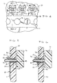
- a connector or other circuit component 31 having a plurality of aligned terminals or pins 33 is passed through correspondingly spaced internally electro-plated holes 35 of a substrate 37. While the substrate 37 is illustrated as oriented vertically in Fig. 5, it will be understood that it may be horizontal or with other orientations, as may be appropriate.
- each row of terminals of the component 31 may be provided with a strip of the clips of Fig. 4, although only one row is shown in Figs. 4 and 5.
- the hole 35 has a metallic surface, as by being electro-plated on its interior, as indicated at 39.
- the plating may extend around onto the flat surface of the substrate 37 to form contact pads, as illustrated at 41. Normally, a slight space 43 is left between the terminal 33 and the plating 39 of the substrate hole 35, into which the molten solder will be drawn.
- the carrier strip 15 is broken away from the individual clips 17 at the breakaway notches 23, leaving the clips 17 in place but soldered to the component terminal, the plating of the hole, and to the contact pad 41. If desired, the carrier strip may be broken away before the soldering is accomplished, although this is not preferred.
- Figure 7 shows an alternate way of using the clips of Figs. 2 and 3.
- a connector or other component 31a is shown having two rows of terminal pins 33 instead of one row as shown in Figure 5.
- the clips 17 are positioned on the component pins 33 before the component pins 33 are inserted into the substrate 37, and are positioned between the component 31a and the substrate 37.
- Heat is supplied as in the case of Figures 5 and 6 to join the pins 33 to the plated hole 39 of the substrate by soldering.
- Figures 8 through 12 show a modified form of the present invention.
- the blank has a carrier strip 115 with indexing holes 113 similar to Figure 1.
- Extending laterally from the carrier strip 115 are the individual solder-holding clips 117.
- each clip blank 117 is joined to the carrier strip 115 by a connecting piece 121 having a breakaway notch 123.
- the individual clip blank 117 includes a body portion 147 having slits 149 extending adjacent the edges of the body portion 147 to form fingers 119 integral at one end with the body portion 147.
- a solder wire 151 (preferably including a solder flux) is laid over the successive body portions 147 of a portion of the array of clips 117 as the array moves along the progressive stamping apparatus. As seen in Figs. 9 to 11, the fingers 119 are then curled around the solder wire 151 to hold it on the body portions 147. After the solder wire 151 is applied and held by the fingers 119, holes 145 are formed as seen in Fig. 9, as by punching through the clip bodies 147. At the same time, the solder wire 151 is separated into two segments straddling each hole 145 and a gap 153 is made in the solder wire 151 between adjoining clip bodies 147 as seen in Figs. 9 and 11.
- each body portion 147 carries two solder masses 125, straddling its hole 145.
- the holes 145 are dimensioned to engage the component terminals 133 frictionally, to position a solder mass on either side of the respective terminal 133 as shown in Fig. 11.
- the solder masses 125 remaining held by each clip body 147 are dimensioned to provide adequate solder for joining each clip 117 to its respective component terminal 133.
- solder-holding clip may be used in the same manner as shown in Figures 6 or 7 or 12.
- the clip 117 may he used to join a component 31 or 131 with any desired further substrate or another component, whether or not substrate 137 is present.
- the clips 117 may be formed with extensions 161 which may be used as terminals or leads to other apparatus.
- the end of each extension 161 may be formed into an edge clip shape 163 for a substrate as shown in Fig. 13 and 14, to permit coupling of the component 131 pins to a further substrate (not shown) parallel to the component 131 or in alignment thereto.
- the further substrate may be perpendicular to substrate 137.
- the end of each extension 161 may be formed for surface mounting to a substrate contact pad, or may have any other desired configuration.
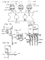
- each solder-holding clip 219 is formed with a pair of sides 201 joined by a back 203.
- Each side 201 has a pair of fingers or tabs 205 extending partially around a solder mass 225, leaving a space 207 between the solder mass 225 and the back 203, for receiving a terminal pin 209 of a connector 211.
- the spacing between the arms 201 is dimensioned to frictionally engage the pins 209.
- the pin 209 passes through a substrate 213, having an internally plated hole and/or a conductive pad to which the pin 209 is to be soldered.
- This form of invention also is adapted for multi-stage progressive stamping.
- an elongated strip of conductive material is stamped as shown in Figure 15 to have a carrier strip 215 with a series of the clips 219 extending laterally therefrom.
- the body is bent into the U-shape shown in Figure 17 to form clip sides 201 each with a pair of tabs or fingers 205.
- a solder wire 225 of a diameter conforming to the separation between the pairs of fingers 205 is laid between the pairs of fingers 205, and the fingers are then bent partially around and staked into the solder wire 225.
- the solder wire 225 is then cut between the clips 219, leaving an amount of solder appropriate for the specific use for the clips.
- a connecting portion 221 serves to join the clip 219 to the carrier strip 215, and is bent with an offset as shown in Figures 17 and 18, so that when assembled to a row of terminals 209, interference is avoided between the terminal pins 209a and 209b and the carrier strip 215.
- the spacing between the clips 209 is correlated to the spacing between the pins 209a or 209b of the connector 211, so that in use a section of the strip of Figure 15 having a number of clips 219 equal to the number of pins 209 in a row of the connector 211, may be inserted over the pins 209 as shown in dashed lines 209 in Figure 15 and also in Figure 18.
- Figure 18 shows connectors 211 illustratively of the dual row type, having terminal pins 209a and 209b equally spaced in the direction perpendicular to the plane of the paper. It will be understood that the present invention may be used with any number of rows of terminal pins, from one row up.
- the connectors 211 may be of the J1 or J2 type, and the substrate 213 may be a PC104 board.
- the terminals 209 may be spaced at 0.100 inch intervals, and the pins may be 0.480 inches long with a 0.025 inch square cross section.
- each clip Upon reflowing, the solder will flow around the pins 209 and by capillary action into the internally plated holes of the substrate 213. After the soldering is completed, each clip has its joining section 221 broken or cut off, as by a notch 223 formed therein.
- solder-holding clips of the present invention are usable not only to solder a connector or other component having non-solder-bearing terminals to through-plated holes of a substrate, but may also be used to solder a lead having any desired terminal configuration to a pin or other terminal of an electrical component.
- Fig. 19 shows the lead clip 219 with its lead 221 bent out at a right angle to terminal pin 209, and terminated in a solder-holding arrangement 250 to permit surface mounting of connector 211 on a substrate (not shown).
- the solder-holding arrangement may have any appropriate construction, such as shown in U.S. Patent No. 4,679,889.
- Fig. 20 therein is shown an alternative embodiment of the present invention, which is similar to that shown in Figs. 1-6.
- clip 317 is provided with two pairs of fingers 319, with one pair of fingers being located on the side of clip 317 adjacent carrier strip 15, and the other pair of fingers being located on the opposite side of clip 317.
- Clip 317 has a generall double I-shape, which may be formed by a progressive stamping operation.
- Two solder portions 321 are positioned laterally across the two pairs of fingers 319. The solder portions 321 may be formed in much the same manner as solder wire 25 (Fig. 2).
- each pair of fingers 319 is then curled around the corresponding solder portion 321 to thereby securely retain the solder portion 321 (Fig. 21).
- the solder sections 321 extend partially into the central aperture in clip 317.
- Fig. 22 therein is shown a connector or other circuit component 31 having a plurality of pins 33, with each of the pins 33 passing through the central aperture of a corresponding clip 317. Because the solder portions 321 extend partially into the central aperture, they act to frictionally engage the inserted pin 33. After the clips 317 are positioned on the connector 31, the pins 33 are subsequently inserted into corresponding holes 35 of a substrate 37.
- a pair of clips 219 (after the removal of connecting portion 221) for soldering a pair of pins 33 on a connector 31 to a pair of contact pads 350 positioned on opposite sides of a substrate 37.
- the pair of clips 219 provide a "straddle mount" between the connector pins 33 and the substate 37.
- the clips 219 are positioned with their solder portions 225 facing each other.
- the connector pins 33 are then inserted into the opposed clips 219, and the substrate is positioned in between clips 219 so as to be frictionally engaged by the opposed solder portions 225. Heat is applied, as described above, to cause the solder to reflow.
- the clips 219 may be provided as a pair of arrays to thereby solder an edge connector to two rows of contact pads, wherein each row is positioned on opposite sides of the substrate 37.
- solder elements 25, 125, 151 and 321 may incorporate customary solder flux to facilitate the proper soldering operation.
- solder-holding clips of the present invention are illustratively described as used with the terminals of a connector, it will be understood that these clips may be used in joining terminals of integrated circuit chips, chip holders, resistors, capacitors and other non-solder bearing electrical components to contact pads or plated holes of printed circuit boards or other substrates.
Landscapes
- Engineering & Computer Science (AREA)
- Manufacturing & Machinery (AREA)
- Mechanical Engineering (AREA)
- Microelectronics & Electronic Packaging (AREA)
- Coupling Device And Connection With Printed Circuit (AREA)
- Manufacturing Of Electrical Connectors (AREA)
- Multi-Conductor Connections (AREA)
Abstract
Claims (30)
- Procédé de jonction d'une broche de borne (33) d'un premier dispositif électronique (31) à une zone conductrice (39) d'un second dispositif (37),
comprenant les étapes suivantes consistant à :prévoir un corps comportant une partie plane munie d'une ouverture pour recevoir le corps sur la broche de borne (33), ce corps comportant une structure de retenue de soudure adjacente à l'ouverture, avec une masse de soudure (25) retenue par la structure ;introduire l'ouverture du corps sur la broche de borne (33) dans une position dans laquelle la soudure (25) est adjacente à la broche de borne (33) et à la zone conductrice (39) ; etfaire refluer puis refroidir la masse de soudure (25) pour souder la broche de borne (33) à la zone conductrice (39). - Procédé selon la revendication 1,
dans lequel
l'ouverture du corps est dimensionnée pour s'engager à friction et retenir le corps dans la position ci-dessus sur la broche de borne (33). - Procédé selon la revendication 1,
dans lequel
la structure de retenue de soudure est adjacente à un premier côté de la seconde ouverture, le corps étant muni d'une seconde structure de retenue de soudure (319) adjacente à un second côté de l'ouverture, le premier côté étant essentiellement opposé au second côté, la seconde structure de retenue de soudure (319) comportant une seconde masse de soudure (321) retenue par celle-ci, les première et seconde masses de soudure (25, 321) étant positionnées pour s'engager à friction et retenir le corps dans la position voulue sur la broche de borne (33). - Procédé selon la revendication 1,
dans lequel
le corps comporte au moins un doigt (19) faisant partie intégrante de celui-ci et destiné à retenir la masse de soudure (25) contre le corps. - Procédé selon la revendication 1,
dans lequel
le corps comporte une paire de doigts (19), un de chaque côté de l'ouverture, et une masse de soudure (25) retenue par chacun des doigts (19) au voisinage de l'ouverture mais sans recouvrir celle-ci. - Procédé selon la revendication 1,
dans lequel
la zone conductrice (39) est un trou plaqué intérieurement dans le second dispositif (37) ; et la masse de soudure (25) est positionnée au voisinage de l'ouverture. - Procédé selon la revendication 1,
dans lequel
la zone conductrice (39) se trouve dans un plan essentiellement perpendiculaire à la broche de borne (33) ; et
la masse de soudure (25) est positionnée au voisinage de la zone (39). - Procédé selon la revendication 1,
comprenant
le positionnement du corps entre les premier et second dispositifs (31, 37). - Procédé selon la revendication 1,
comprenant en outre les étapes suivantes consistant à :positionner la broche de borne (33) et l'étendre au-delà de l'ouverture ; puispositionner ensuite le corps sur la broche de borne (33) au voisinage de cette ouverture. - Procédé selon la revendication 1,
dans lequel
une seule masse de soudure (25) est positionnée de chaque côté de l'ouverture mais sans la recouvrir. - Procédé selon la revendication 1,
dans lequel
le corps fait partie d'une pince (17) et l'ouverture s'engage à friction et retient le corps sur la broche de borne (33), ce corps comportant un prolongement (161) qui est soudé au second dispositif (37). - Procédé selon la revendication 3,
dans lequel
l'ouverture du corps est introduite sur la broche de borne (33) de façon que les première et seconde masses de soudure (25, 321) soient adjacentes à cette broche de borne (33) et à la zone conductrice (39), le procédé comprenant en outre l'étape suivante consistant à :faire refluer puis refroidir les masses de soudure (25, 321) pour souder la broche de borne (33) à la zone conductrice (39) ; etla pince (17) comporte un prolongement (161) et soude le second dispositif à ce prolongement (161). - Procédé selon la revendication 1,
dans lequelle corps est une bande de matériau allongée et une section, s'étendant longitudinalement, de la bande fournit une bande porteuse (15), le corps faisant partie d'une pince (17, 319),la bande comprend un réseau de pinces (17) faisant partie intégrante de la bande porteuse (15), en étant espacées le long de cette bande porteuse (15) en correspondance avec l'espacement d'un réseau de trous plaqués (35) formés dans le second dispositif (37), la zone conductrice (39) comprenant un réseau de broches de borne (33) de façon que le réseau de pinces (17, 319) soit introduit sur les broches de borne correspondantes (33) du réseau de broches de borne (33) dans une position telle que chaque masse de soudure (25) soit adjacente à un trou plaqué respectif (35) et que chaque corps de pince soit retenu à friction par sa broche respective (33) dans la position voulue, le réseau de broches de borne (33) étant introduit dans les trous plaqués (35) du second dispositif (37), de façon que chaque masse de soudure (25) soit adjacente à l'un, respectif, des trous plaqués (35);on fait refluer les masses de soudure (25) pour les faire s'écouler, par un effet de capillarité, dans chaque trou plaqué (35) contenant une broche de borne respective (33) ; eton laisse refroidir la soudure (25) pour joindre chaque broche de borne (33) à son trou plaqué respectif (35). - Procédé selon la revendication 1,
comprenant en outre les étapes suivantes consistant à :donner au corps une seconde structure de retenue de soudure au voisinage d'un second côté de l'ouverture, cette structure de retenue de soudure étant adjacente à un premier côté de l'ouverture, chacune des structures de retenue de soudure comportant une masse de soudure (25, 325) retenue par celle-ci ;le corps est une bande de matériau allongée munie d'une section s'étendant longitudinalement pour former une bande porteuse (15), le corps faisant partie d'une pince (17) ;la bande comprend un réseau de pinces (17, 319) faisant partie intégrante de la bande porteuse (15), en étant espacées le long de cette bande porteuse (15) en correspondance avec l'espacement d'un réseau de trous plaqués (35) formés dans le second dispositif (37), la zone conductrice (39) comprenant un réseau de broches de borne (33) de façon que le réseau de pinces (17, 319) soit introduit sur les broches de borne correspondantes (33) du réseau de broches de borne (33) dans une position telle que chaque masse de soudure (25, 325) soit adjacente à un trou plaqué respectif (35) et que chaque corps de pince soit retenu à friction par sa broche de borne respective (33) dans la position voulue, le réseau de broches de borne (33) étant introduit dans les trous plaqués (35) du second dispositif (37), de façon que chaque masse de soudure (25, 325) soit adjacente à l'un, respectif, des trous plaqués (35) ;on fait refluer les masses de soudure (25, 325) pour faire s'écouler la soudure, par un effet de capillarité, dans chaque trou plaqué (35) contenant une broche de borne respective (33) ; eton laisse refroidir la soudure (25, 325) pour joindre chaque broche de borne (33) à son trou plaqué respectif (35). - Procédé selon la revendication 13,
comprenant en outre les étapes consistant à :introduire les pinces (17, 319) sur les broches de borne (33) après l'introduction de ces broches de borne (33) dans leurs trous de substrat respectifs (35) ; etfaire refluer ensuite la masse de soudure (25). - Procédé selon la revendication 15,
comprenant en outre les étapes consistant à :introduire le réseau de pinces (17, 319) sur les broches de borne (33) pour engager à friction les pinces (17, 319) sur ces broches de borne (33) ; etintroduire ensuite les broches de borne (33) dans leurs trous de substrat respectifs (35). - Procédé selon la revendication 1,
dans lequel
le corps est joint à la broche de borne (33) électriquement et mécaniquement. - Procédé selon la revendication 17,
comprenant en outre l'étage consistant à :joindre simultanément la pince (17) au second dispositif (37). - Procédé selon la revendication 1,
comprenant en outre
l'utilisation d'une seconde structure de retenue de soudure du côté de l'ouverture qui est opposé à la structure de retenue de soudure, chacune de ces structures comprenant un doigt (19) faisant séparément partie intégrante du corps,
dans lequel
la masse de soudure (25, 325) est retenue par les structures en déposant un fil de soudure sur le corps au-dessus de l'ouverture et de chaque côté de celle-ci, sur les doigts (19), en courbant les doigts (19) sur le fil de soudure (25, 325), et en retirant la soudure (25, 325) qui recouvre l'ouverture. - Pince à retenue de soudure (17) pour se relier à une broche de borne (33) d'un dispositif électrique (31), la pince à retenue de soudure (17) comportant un corps (11) muni d'une partie plane percée d'une ouverture destinée à recevoir la broche de borne (33), cette ouverture étant dimensionnée pour recevoir le corps (11) sur la broche de borne (33),
le corps (11) comportant une structure de retenue de soudure adjacente à l'ouverture, et une masse de soudure (25) retenue par la structure. - Pince (17) selon la revendication 20,
dans laquelle
cette pince (17) se trouve dans un plan essentiellement parallèle à une zone conductrice (39) d'un second dispositif (37). - Pince (17) selon la revendication 20,
dans laquelle
le corps comporte au moins un doigt (19) faisant partie intégrante de celui-ci et retenant la masse de soudure (25) contre ce corps. - Pince (17) selon la revendication 22,
dans laquelle
le corps comporte une paire de doigts (19) faisant partie intégrante de celui-ci, avec un doigt le long de chaque bord du corps, ces doigts (19) retenant au moins une masse de soudure (25) contre le corps. - Pince (17) selon la revendication 23,
dans laquellechacun des doigts (19) se trouve sur un côté respectif de l'ouverture, etla masse de soudure (25) est retenue par chacun de ces doigts (19) au voisinage de l'ouverture mais sans la recouvrir. - Pince (17) selon la revendication 20,
dans laquellele corps comporte une partie munie d'une structure en forme de U avec une paire de côtés espacés reliés par une partie de dos ;la masse de soudure (25) est retenue par ces côtés ; etl'ouverture est formée par la partie de dos et les côtés. - Pince (17) selon la revendication 20,
dans laquellele corps comporte une structure en forme de U munie d'une paire de côtés (201) et d'un dos (203) reliant les côtés (201), chaque côté (201) comportant une paire de pattes espacées (205) ; etla soudure (25) est retenue entre la paire de pattes (205) de chaque paire de côtés (201). - Pince (17) selon la revendication 26,
dans laquelle
la soudure (25) est espacée du dos de la pince (17) pour former, avec les côtés de la pince (17), les ouvertures de réception de borne entre ceux-ci. - Réseau de pinces à retenue de soudure (17, 319) selon la revendication 20, pour se joindre à un réseau de broches de borne (33), ce réseau de pinces (17, 319) comprenant une bande de matériau allongée,
une section s'étendant longitudinalement de cette bande formant une bande porteuse (15), les pinces (17) faisant partie intégrante de la bande porteuse (15) et partant latéralement de celle-ci, les pinces étant espacées de manière correspondante à celle du réseau de broches de borne (33). - Réseau de pinces (17) selon la revendication 26,
dans lequel
chacun des corps comporte une seconde structure de retenue de soudure positionnée du côté opposé de l'ouverture, comme structure de retenue de soudure, chacune de ces structures retenant une masse de soudure (25, 325), ces masses de soudure (25, 325) étant positionnées pour s'engager à friction et pour retenir chacune des pinces (17, 319) de chacune des broches de borne (33). - Réseau de pinces (17) selon la revendication 26,
comprenant en outre
un fil conducteur (161) partant de chaque partie de corps pour former une borne vers un autre dispositif.
Applications Claiming Priority (5)
| Application Number | Priority Date | Filing Date | Title |
|---|---|---|---|
| US620595P | 1995-11-03 | 1995-11-03 | |
| US6205P | 1995-11-03 | ||
| US726960 | 1996-10-07 | ||
| US08/726,960 US5875546A (en) | 1995-11-03 | 1996-10-07 | Method of forming solder-holding clips for applying solder to connectors |
| PCT/US1996/017704 WO1997016870A1 (fr) | 1995-11-03 | 1996-11-01 | Pince a retenue de soudure pour l'application de soudure a des connecteurs |
Publications (3)
| Publication Number | Publication Date |
|---|---|
| EP0860033A1 EP0860033A1 (fr) | 1998-08-26 |
| EP0860033A4 EP0860033A4 (fr) | 2000-01-26 |
| EP0860033B1 true EP0860033B1 (fr) | 2003-03-05 |
Family
ID=26675316
Family Applications (1)
| Application Number | Title | Priority Date | Filing Date |
|---|---|---|---|
| EP96937899A Expired - Lifetime EP0860033B1 (fr) | 1995-11-03 | 1996-11-01 | Pince a retenue de soudure pour l'application de soudure a des connecteurs |
Country Status (6)
| Country | Link |
|---|---|
| US (4) | US5875546A (fr) |
| EP (1) | EP0860033B1 (fr) |
| CN (2) | CN1244183C (fr) |
| AU (1) | AU7553696A (fr) |
| DE (1) | DE69626536T2 (fr) |
| WO (1) | WO1997016870A1 (fr) |
Families Citing this family (32)
| Publication number | Priority date | Publication date | Assignee | Title |
|---|---|---|---|---|
| US6543129B2 (en) * | 1995-11-03 | 2003-04-08 | Teka Interconnections Systems, Inc. | Solder-bearing contacts and method of manufacture thereof and use in a solder ball grid array connector |
| TW406454B (en) | 1996-10-10 | 2000-09-21 | Berg Tech Inc | High density connector and method of manufacture |
| US6000977A (en) * | 1997-09-04 | 1999-12-14 | Mcdonnell Douglas Corporation | Electrical connection devices for composite structures having externally accessible ports |
| AU7609500A (en) * | 1999-09-20 | 2001-04-24 | Nas Interplex Industries Inc. | Solder-bearing wafer for use in soldering operations |
| US20020052146A1 (en) * | 1999-11-05 | 2002-05-02 | James Keith Custer | Circuit board apparatus with pin connectors |
| AU2000267992A1 (en) * | 2000-08-23 | 2002-03-04 | John K Shannon | Solder-in-place axial-type connector |
| US6739881B2 (en) * | 2001-05-31 | 2004-05-25 | Trw Inc. | High integration electronic assembly and method |
| JP3413186B2 (ja) * | 2001-07-13 | 2003-06-03 | モルデック株式会社 | コネクタ及びその製造方法 |
| JP2003045509A (ja) * | 2001-08-01 | 2003-02-14 | Tokai Rika Co Ltd | コネクタのプリント回路基板への取付方法及びコネクタ |
| WO2003085697A2 (fr) * | 2002-04-01 | 2003-10-16 | Interplex Nas, Inc. | Articles porteurs de brasure et procede de retention d'une masse de brasure sur ces articles |
| US6780028B1 (en) * | 2002-12-06 | 2004-08-24 | Autosplice Systems Inc. | Solder reserve transfer device and process |
| US7001190B2 (en) * | 2004-04-26 | 2006-02-21 | Tyco Electronics Corporation | Repairable ball grid array contact |
| US6955545B1 (en) | 2004-04-27 | 2005-10-18 | Tyco Electronics Corporation | Two piece ball grid array |
| US6979238B1 (en) * | 2004-06-28 | 2005-12-27 | Samtec, Inc. | Connector having improved contacts with fusible members |
| WO2006032035A1 (fr) * | 2004-09-15 | 2006-03-23 | Molex Incorporated | Procede destine a fixer un element de brasure a un contact et ensemble contact ainsi forme |
| US7419084B2 (en) * | 2004-11-24 | 2008-09-02 | Xerox Corporation | Mounting method for surface-mount components on a printed circuit board |
| DE102005013599B4 (de) * | 2005-03-24 | 2009-06-10 | Erni Electronics Gmbh | Verfahren zum Reparaturlöten vielpoliger Miniatur-Steckverbinder |
| US8991680B1 (en) * | 2005-05-25 | 2015-03-31 | Alfred E. Mann Foundation For Scientific Research | Method of manufacture of an electrode array |
| DE102007014337B4 (de) * | 2007-03-26 | 2017-07-06 | Robert Bosch Gmbh | Verfahren zum Bestücken eines Kontaktierungselementes mit einem elektrischen Bauelement sowie ein Kontaktierungselement mit einem elektrischen Bauelement |
| ITRM20070237A1 (it) * | 2007-04-24 | 2008-10-25 | Augusto Vincenzi | Assieme di terminali elettrici |
| CN201075553Y (zh) * | 2007-07-17 | 2008-06-18 | 番禺得意精密电子工业有限公司 | 电连接器及使用该电连接器的电连接装置 |
| US20100173507A1 (en) * | 2009-01-07 | 2010-07-08 | Samtec, Inc. | Electrical connector having multiple ground planes |
| US8497429B2 (en) * | 2009-03-18 | 2013-07-30 | Interplex Industries, Inc. | Planar contact with solder |
| US8425239B2 (en) | 2009-07-09 | 2013-04-23 | Tyco Electronics Corporation | Electrical connector for a solar module assembly |
| US8616926B2 (en) * | 2009-08-17 | 2013-12-31 | Norman R. Byrne | Solid wire terminal |
| US7837522B1 (en) * | 2009-11-12 | 2010-11-23 | Samtec, Inc. | Electrical contacts with solder members and methods of attaching solder members to electrical contacts |
| CN102820267A (zh) * | 2011-06-10 | 2012-12-12 | 钰桥半导体股份有限公司 | 插销式半导体封装堆栈结构 |
| CN203180152U (zh) * | 2013-02-07 | 2013-09-04 | 番禺得意精密电子工业有限公司 | 电连接器 |
| CN107431299B (zh) | 2015-02-27 | 2019-05-21 | 诺曼·R·伯恩 | 用于汇流条和刀片端子的电触点接收器 |
| EP3142199B1 (fr) * | 2015-09-10 | 2020-04-15 | TE Connectivity Germany GmbH | Pièce de tôle à géométrie de languette de connexion améliorée et méthode de production associée |
| WO2017101879A1 (fr) * | 2015-12-18 | 2017-06-22 | 深圳市敏杰电子科技有限公司 | Appareil de détection, terminal de perçage, bande d'estampage et procédé correspondant |
| JP7272011B2 (ja) * | 2019-02-27 | 2023-05-12 | 住友電装株式会社 | 基板用コネクタ |
Family Cites Families (21)
| Publication number | Priority date | Publication date | Assignee | Title |
|---|---|---|---|---|
| US3905665A (en) * | 1971-07-27 | 1975-09-16 | Amp Inc | Electrical contact structure and assembly method |
| US3750252A (en) * | 1972-05-01 | 1973-08-07 | Du Pont | Solder terminal strip |
| US3932934A (en) * | 1974-09-16 | 1976-01-20 | Amp Incorporated | Method of connecting terminal posts of a connector to a circuit board |
| US4203648A (en) * | 1977-08-15 | 1980-05-20 | North American Specialties Corp. | Solder bearing terminal |
| US4120558A (en) * | 1977-08-15 | 1978-10-17 | North American Specialties Corporation | Solder bearing terminal |
| US4302067A (en) * | 1980-04-18 | 1981-11-24 | Western Electric Company, Incorporated | Edge connectors for circuit cards and methods of assembly |
| US4802862A (en) | 1981-03-30 | 1989-02-07 | North American Specialties Corporation | Solderable electrical contact |
| US4422128A (en) * | 1981-08-06 | 1983-12-20 | General Motors Corporation | Push-on terminal clip and assembly |
| US4605278A (en) * | 1985-05-24 | 1986-08-12 | North American Specialties Corporation | Solder-bearing leads |
| US4556276A (en) * | 1983-05-06 | 1985-12-03 | At&T Bell Laboratories | Solder beams leads |
| US4597625A (en) | 1984-07-25 | 1986-07-01 | North American Specialties Corporation | Electrical connector |
| US5052954A (en) * | 1985-05-24 | 1991-10-01 | North American Specialties Corporation | Solder-bearing terminal pin and lead |
| US4883435A (en) * | 1985-05-24 | 1989-11-28 | North American Specialties Corporation | Solder-bearing terminal pin and lead |
| US5139448A (en) | 1985-05-24 | 1992-08-18 | North American Specialties Corporation | Solder-bearing lead |
| US4663815A (en) * | 1985-06-21 | 1987-05-12 | Associated Enterprises, Inc. | A method and apparatus for surface mount compatible connector system with mechanical integrity |
| US4641426A (en) * | 1985-06-21 | 1987-02-10 | Associated Enterprises, Inc. | Surface mount compatible connector system with mechanical integrity |
| US4884335A (en) * | 1985-06-21 | 1989-12-05 | Minnesota Mining And Manufacturing Company | Surface mount compatible connector system with solder strip and mounting connector to PCB |
| US4767344A (en) * | 1986-08-22 | 1988-08-30 | Burndy Corporation | Solder mounting of electrical contacts |
| US5357074A (en) * | 1993-08-17 | 1994-10-18 | The Whitaker Corporation | Electrical interconnection device |
| US5441430A (en) * | 1994-04-06 | 1995-08-15 | North American Specialties Corporation | Electrical lead for surface mounting of substrates |
| US5490788A (en) * | 1994-11-01 | 1996-02-13 | Emc Technology, Inc. | Surface mount terminal for electrical component |
-
1996
- 1996-10-07 US US08/726,960 patent/US5875546A/en not_active Expired - Lifetime
- 1996-11-01 CN CNB021045755A patent/CN1244183C/zh not_active Expired - Fee Related
- 1996-11-01 WO PCT/US1996/017704 patent/WO1997016870A1/fr not_active Ceased
- 1996-11-01 CN CN96198096A patent/CN1096123C/zh not_active Expired - Fee Related
- 1996-11-01 EP EP96937899A patent/EP0860033B1/fr not_active Expired - Lifetime
- 1996-11-01 AU AU75536/96A patent/AU7553696A/en not_active Abandoned
- 1996-11-01 DE DE69626536T patent/DE69626536T2/de not_active Expired - Lifetime
-
1997
- 1997-12-29 US US08/998,915 patent/US6099365A/en not_active Expired - Lifetime
- 1997-12-29 US US08/998,917 patent/US6402574B2/en not_active Expired - Lifetime
-
2002
- 2002-01-02 US US10/038,418 patent/US6494754B2/en not_active Expired - Lifetime
Also Published As
| Publication number | Publication date |
|---|---|
| CN1096123C (zh) | 2002-12-11 |
| US20010041481A1 (en) | 2001-11-15 |
| EP0860033A1 (fr) | 1998-08-26 |
| DE69626536T2 (de) | 2003-11-06 |
| WO1997016870A1 (fr) | 1997-05-09 |
| CN1201556A (zh) | 1998-12-09 |
| US6402574B2 (en) | 2002-06-11 |
| US20020058446A1 (en) | 2002-05-16 |
| CN1438734A (zh) | 2003-08-27 |
| US6099365A (en) | 2000-08-08 |
| US6494754B2 (en) | 2002-12-17 |
| CN1244183C (zh) | 2006-03-01 |
| US5875546A (en) | 1999-03-02 |
| AU7553696A (en) | 1997-05-22 |
| EP0860033A4 (fr) | 2000-01-26 |
| DE69626536D1 (de) | 2003-04-10 |
Similar Documents
| Publication | Publication Date | Title |
|---|---|---|
| US5875546A (en) | Method of forming solder-holding clips for applying solder to connectors | |
| WO1997016870A9 (fr) | Pince a retenue de soudure pour l'application de soudure a des connecteurs | |
| US4679889A (en) | Solder-bearing leads | |
| KR940002662Y1 (ko) | 납땜 지지 터미널 | |
| EP0524248B1 (fr) | Fil porteur de metal de brasage | |
| US5139448A (en) | Solder-bearing lead | |
| EP0303873B1 (fr) | Dispositif de conducteur | |
| US4728305A (en) | Solder-bearing leads | |
| US6543129B2 (en) | Solder-bearing contacts and method of manufacture thereof and use in a solder ball grid array connector | |
| EP0754356B1 (fr) | Connecteurs electriques pour montage en surface de substrats | |
| EP0806063B1 (fr) | Rangee de conducteurs assembles a des composants electriques et methode correspondante d'assemblage | |
| US5090926A (en) | Solderable lead | |
| US4486066A (en) | Connector and clip therefor | |
| CA2236464C (fr) | Pince a retenue de soudure pour l'application de soudure a des connecteurs | |
| AU583396B2 (en) | Solder bearing leads | |
| JP3582883B2 (ja) | 面実装コネクタ |
Legal Events
| Date | Code | Title | Description |
|---|---|---|---|
| PUAI | Public reference made under article 153(3) epc to a published international application that has entered the european phase |
Free format text: ORIGINAL CODE: 0009012 |
|
| 17P | Request for examination filed |
Effective date: 19980603 |
|
| AK | Designated contracting states |
Kind code of ref document: A1 Designated state(s): DE FR GB IT |
|
| A4 | Supplementary search report drawn up and despatched |
Effective date: 19991210 |
|
| AK | Designated contracting states |
Kind code of ref document: A4 Designated state(s): DE FR GB IT |
|
| RIC1 | Information provided on ipc code assigned before grant |
Free format text: 7H 01R 9/09 A, 7H 01R 4/02 B, 7H 01R 43/02 B |
|
| 17Q | First examination report despatched |
Effective date: 20000713 |
|
| RIC1 | Information provided on ipc code assigned before grant |
Free format text: 7H 01R 12/24 A, 7H 01R 12/32 B, 7H 01R 4/02 B, 7H 01R 43/02 B |
|
| GRAG | Despatch of communication of intention to grant |
Free format text: ORIGINAL CODE: EPIDOS AGRA |
|
| GRAG | Despatch of communication of intention to grant |
Free format text: ORIGINAL CODE: EPIDOS AGRA |
|
| GRAH | Despatch of communication of intention to grant a patent |
Free format text: ORIGINAL CODE: EPIDOS IGRA |
|
| RAP1 | Party data changed (applicant data changed or rights of an application transferred) |
Owner name: NAS INTERPLEX, INC. |
|
| GRAH | Despatch of communication of intention to grant a patent |
Free format text: ORIGINAL CODE: EPIDOS IGRA |
|
| GRAA | (expected) grant |
Free format text: ORIGINAL CODE: 0009210 |
|
| AK | Designated contracting states |
Designated state(s): DE FR GB IT |
|
| PG25 | Lapsed in a contracting state [announced via postgrant information from national office to epo] |
Ref country code: IT Free format text: LAPSE BECAUSE OF FAILURE TO SUBMIT A TRANSLATION OF THE DESCRIPTION OR TO PAY THE FEE WITHIN THE PRE;WARNING: LAPSES OF ITALIAN PATENTS WITH EFFECTIVE DATE BEFORE 2007 MAY HAVE OCCURRED AT ANY TIME BEFORE 2007. THE CORRECT EFFECTIVE DATE MAY BE DIFFERENT FROM THE ONE RECORDED.SCRIBED TIME-LIMIT Effective date: 20030305 Ref country code: FR Free format text: LAPSE BECAUSE OF NON-PAYMENT OF DUE FEES Effective date: 20030305 |
|
| REG | Reference to a national code |
Ref country code: GB Ref legal event code: FG4D |
|
| REF | Corresponds to: |
Ref document number: 69626536 Country of ref document: DE Date of ref document: 20030410 Kind code of ref document: P |
|
| PG25 | Lapsed in a contracting state [announced via postgrant information from national office to epo] |
Ref country code: GB Free format text: LAPSE BECAUSE OF NON-PAYMENT OF DUE FEES Effective date: 20031101 |
|
| PLBE | No opposition filed within time limit |
Free format text: ORIGINAL CODE: 0009261 |
|
| STAA | Information on the status of an ep patent application or granted ep patent |
Free format text: STATUS: NO OPPOSITION FILED WITHIN TIME LIMIT |
|
| EN | Fr: translation not filed | ||
| 26N | No opposition filed |
Effective date: 20031208 |
|
| GBPC | Gb: european patent ceased through non-payment of renewal fee |
Effective date: 20031101 |
|
| PGFP | Annual fee paid to national office [announced via postgrant information from national office to epo] |
Ref country code: DE Payment date: 20091130 Year of fee payment: 14 |
|
| REG | Reference to a national code |
Ref country code: DE Ref legal event code: R119 Ref document number: 69626536 Country of ref document: DE Effective date: 20110601 Ref country code: DE Ref legal event code: R119 Ref document number: 69626536 Country of ref document: DE Effective date: 20110531 |
|
| PG25 | Lapsed in a contracting state [announced via postgrant information from national office to epo] |
Ref country code: DE Free format text: LAPSE BECAUSE OF NON-PAYMENT OF DUE FEES Effective date: 20110531 |