EP0862061B1 - Procédé et dispositif de contrôle de cartes de circuit - Google Patents
Procédé et dispositif de contrôle de cartes de circuit Download PDFInfo
- Publication number
- EP0862061B1 EP0862061B1 EP98103453A EP98103453A EP0862061B1 EP 0862061 B1 EP0862061 B1 EP 0862061B1 EP 98103453 A EP98103453 A EP 98103453A EP 98103453 A EP98103453 A EP 98103453A EP 0862061 B1 EP0862061 B1 EP 0862061B1
- Authority
- EP
- European Patent Office
- Prior art keywords
- circuit board
- signal
- inspection apparatus
- terminal
- terminals
- Prior art date
- Legal status (The legal status is an assumption and is not a legal conclusion. Google has not performed a legal analysis and makes no representation as to the accuracy of the status listed.)
- Expired - Lifetime
Links
- 238000007689 inspection Methods 0.000 title claims description 66
- 238000000034 method Methods 0.000 title description 27
- 230000008878 coupling Effects 0.000 claims description 14
- 238000010168 coupling process Methods 0.000 claims description 14
- 238000005859 coupling reaction Methods 0.000 claims description 14
- 230000000630 rising effect Effects 0.000 claims description 12
- 238000012360 testing method Methods 0.000 claims description 9
- 239000000523 sample Substances 0.000 description 24
- 238000001514 detection method Methods 0.000 description 14
- 239000003990 capacitor Substances 0.000 description 9
- 239000011295 pitch Substances 0.000 description 6
- 230000008569 process Effects 0.000 description 6
- 238000004519 manufacturing process Methods 0.000 description 4
- 239000000463 material Substances 0.000 description 4
- 230000004913 activation Effects 0.000 description 3
- 230000004044 response Effects 0.000 description 3
- 239000000758 substrate Substances 0.000 description 3
- 239000004593 Epoxy Substances 0.000 description 2
- 239000004020 conductor Substances 0.000 description 2
- 239000011521 glass Substances 0.000 description 2
- 230000001788 irregular Effects 0.000 description 2
- 230000008054 signal transmission Effects 0.000 description 2
- 230000001052 transient effect Effects 0.000 description 2
- 230000003213 activating effect Effects 0.000 description 1
- 230000008859 change Effects 0.000 description 1
- 239000002131 composite material Substances 0.000 description 1
- 230000001419 dependent effect Effects 0.000 description 1
- 230000000694 effects Effects 0.000 description 1
- 230000005684 electric field Effects 0.000 description 1
- 230000005611 electricity Effects 0.000 description 1
- 238000001914 filtration Methods 0.000 description 1
- 238000003780 insertion Methods 0.000 description 1
- 230000037431 insertion Effects 0.000 description 1
- 238000009413 insulation Methods 0.000 description 1
- 230000010354 integration Effects 0.000 description 1
- 230000001678 irradiating effect Effects 0.000 description 1
- 238000003825 pressing Methods 0.000 description 1
- 230000009467 reduction Effects 0.000 description 1
- 238000000926 separation method Methods 0.000 description 1
Images






Classifications
-
- G—PHYSICS
- G01—MEASURING; TESTING
- G01R—MEASURING ELECTRIC VARIABLES; MEASURING MAGNETIC VARIABLES
- G01R31/00—Arrangements for testing electric properties; Arrangements for locating electric faults; Arrangements for electrical testing characterised by what is being tested not provided for elsewhere
- G01R31/28—Testing of electronic circuits, e.g. by signal tracer
- G01R31/2801—Testing of printed circuits, backplanes, motherboards, hybrid circuits or carriers for multichip packages [MCP]
- G01R31/2805—Bare printed circuit boards
-
- G—PHYSICS
- G01—MEASURING; TESTING
- G01R—MEASURING ELECTRIC VARIABLES; MEASURING MAGNETIC VARIABLES
- G01R31/00—Arrangements for testing electric properties; Arrangements for locating electric faults; Arrangements for electrical testing characterised by what is being tested not provided for elsewhere
- G01R31/28—Testing of electronic circuits, e.g. by signal tracer
- G01R31/2801—Testing of printed circuits, backplanes, motherboards, hybrid circuits or carriers for multichip packages [MCP]
- G01R31/281—Specific types of tests or tests for a specific type of fault, e.g. thermal mapping, shorts testing
- G01R31/2812—Checking for open circuits or shorts, e.g. solder bridges; Testing conductivity, resistivity or impedance
-
- G—PHYSICS
- G01—MEASURING; TESTING
- G01R—MEASURING ELECTRIC VARIABLES; MEASURING MAGNETIC VARIABLES
- G01R31/00—Arrangements for testing electric properties; Arrangements for locating electric faults; Arrangements for electrical testing characterised by what is being tested not provided for elsewhere
- G01R31/28—Testing of electronic circuits, e.g. by signal tracer
- G01R31/302—Contactless testing
- G01R31/312—Contactless testing by capacitive methods
-
- H—ELECTRICITY
- H05—ELECTRIC TECHNIQUES NOT OTHERWISE PROVIDED FOR
- H05K—PRINTED CIRCUITS; CASINGS OR CONSTRUCTIONAL DETAILS OF ELECTRIC APPARATUS; MANUFACTURE OF ASSEMBLAGES OF ELECTRICAL COMPONENTS
- H05K1/00—Printed circuits
- H05K1/02—Details
- H05K1/0266—Marks, test patterns or identification means
-
- H—ELECTRICITY
- H05—ELECTRIC TECHNIQUES NOT OTHERWISE PROVIDED FOR
- H05K—PRINTED CIRCUITS; CASINGS OR CONSTRUCTIONAL DETAILS OF ELECTRIC APPARATUS; MANUFACTURE OF ASSEMBLAGES OF ELECTRICAL COMPONENTS
- H05K1/00—Printed circuits
- H05K1/02—Details
- H05K1/11—Printed elements for providing electric connections to or between printed circuits
Definitions
- the present invention relates to a circuit board inspection apparatus and method, and in particular, to the inspection of the continuity of wiring formed on a circuit board.
- a method for contacting probes with both ends of a printed pattern is one of the methods for inspecting the continuity of a printed pattern formed on a printed circuit board.
- the continuity of the printed pattern can be inspected by checking whether a predetermined current flows when a voltage is applied between both probes.
- the non-contact sensor using a sine-wave alternating current must execute filtering or include a wave detector to reduce the effects of noise such as hum components, approximately several tens of milliseconds were required to inspect a single printed pattern. If several thousand inspections are carried out for a single circuit board, several tens of seconds are required to inspect that circuit board.
- This inspection method connects terminals 20a and 20b of an inspection apparatus 20, a printed pattern 22, and a reference potential surface 24 formed to ensure insulation from the printed pattern 22, respectively, and applies a direct current to the terminal 20a for an inspection, as shown in Figure 15A. That is, this method determines the acceptability of the printed pattern 22 based on a transient current flowing through a capacitor formed between the printed pattern 22 and the reference potential surface 24.
- this method may fail to detect this open-circuit.
- both printed patterns 22a and 22b are open-circuited and short-circuited, this method may also fail to detect this condition.
- this method must wait for this capacitor with a relatively large capacity to be almost fully charged, which prevents significant reductions in the inspection time.
- JP-854448 describes a system for substrate inspection having a non-contact voltage feeding apparatus.
- the feeding apparatus includes a feed control element having a laminated structure as a light probe.
- a voltage is applied to the light probe disposed on the feeding side of the circuit pattern to be inspected by irradiating the light probe with a laser beam.
- An electrostatic capacitance coupling under a non-contact system is provided on the detection side, and an electrical condition of the coupling is extracted from the circuit and a waveform processing is performed on the detected signals so as to make it possible to test respective conductive paths of the circuit pattern.
- EP-A-0633478 discloses a device for testing encased integrated circuit devices mounted on a circuit board. For this purpose, rectangular voltage pulses are provided to one or more pins of an encased integrated circuit device, while other pins of the circuit are grounded. The electric field generated inside the casing of the integrated circuit device is detected capacitively, where a measuring signal m(t) is output and compared to a threshold value. If the measuring signal is below the threshold, then a faulty connection is determined.
- the term "circuit board” refers to a substrate on which wiring can be or has been formed and is not limited in terms of its material, structure, shape, or sizes.
- the circuit board includes, for example, a glass epoxy circuit board, a film-like circuit board, and a package on which circuit elements such as a CPU are mounted. It also includes a composite circuit board comprising sockets on a glass epoxy circuit board and a circuit board on which circuit elements are mounted.
- wiring refers to a conductor that is used to conduct electricity and is not limited in terms of its material, structure, shape, or sizes. This term is a concept including printed patterns, through-holes, and pins that are formed on the circuit board as well as the conducting section of electric cords, sockets, connectors, and pins attached to the circuit board.
- one end of the wiring or “the other end of the wiring” refer to a point of the wiring to or from which an inspection signal is input or output and it is not limited in terms of its material, structure, shape, or sizes.
- This term includes an electric connection point to which a different component is connected such as an inspection-end or a connector-connection-end of the printed pattern, a connection pin, a pad to which a bonding wire is connected, a pad to which a circuit element or a socket is connected, an insertion portion formed in a socket mounted on the circuit board, and an I/O end of a connector, as well as an arbitrary point within the wiring.
- Coupled refers to coupling two or more members together so that a signal can be transmitted among the members while they are insulated from one another. It also includes coupling by means of electrostatic capacity or inductance.
- signal refers to a signal used for inspections and is a concept including either a voltage or a current. It also includes alternating currents such as sine waves, a direct signal, a rectangular and a triangular signals, and a pulse signal.
- the expression "based on a voltage generated between the first and the second terminals" means that something is based on a voltage generated between the first and second terminals or a physical quantity corresponding to or associated with the voltage.
- this physical quantity includes not only the voltage but also a current corresponding to or associated with the voltage, and its integrated and differential values.
- detection of the continuity of the wiring refers to a concept that includes the detection of an open-or a short-circuit in the wiring and the detection of the resistance value of wiring such as a semi-open-circuit.
- group refers to a set composed of one or two or more elements.
- signal with rapid changes refers to a signal such as a voltage or a current that is subjected to frequent changes per unit time, and it includes, for example, a direct signal having a step-like rising or falling edge, a triangular and a rectangular signal, and a pulse signal.
- electrode section refers to a conductor constituting an electrode on the second electrode side when electrostatic capacity is used for coupling and is not limited in terms of its material, structure, shape, or size.
- the circuit board inspection apparatus couples the second terminal to the other end of the wiring without contact.
- expensive probes that offer a fine pitch and that are otherwise required for a circuit board on which the other end of the wiring is densely disposed are not necessary.
- This configuration also avoids damage to the other end of the wiring.
- anisotropic conducting rubber is not used, a signal can be transmitted between the other end of the wiring and the second terminal even if there is a resist at the other end of the wiring.
- the continuity of the wiring is detected based on a voltage generated between the first terminal connected or coupled to one end of the wiring and the second terminal coupled to the other end of the wiring. Consequently, an open-circuit can be detected regardless of the position of the open-circuit on the wiring or the presence of a short-circuit in the wiring.
- this circuit board inspection apparatus is characterized in that the predetermined signal has sharp rising or falling edges. Consequently, when the signal is delivered, the voltage generated between the first and the second terminals is rapidly changed in response to changes in this signal. As a result, these rapid changes can be detected to determine the continuity of the wiring in order to conduct inspections promptly. In addition, the apparatus and method is thus unlikely to be affected by noise.
- the circuit board inspection apparatus has the feature that the second terminal is capacitively coupled to the other end of the wiring. Consequently, reliable inspections can be conducted using a simple configuration.
- the apparatus is also characterized in that it determines the continuity of the wiring based on the maximum voltage generated between the first and the second terminals after a signal used for the inspection has changed rapidly.
- the maximum voltage is generated almost simultaneously with a rapid change in the signal. As a result, the continuity of the wiring can be determined in a very short time.
- the circuit board inspection apparatus can have the feature that the continuity of the wire identified by the second terminal and the selected first terminal by switching the first switch means.
- the desired wire can be identified and inspected by connecting or coupling the relevant first terminal to one end of a plurality of wires to be inspected, and then switching the first switch means as required.
- the first terminal or the inspected circuit board need not be moved during an inspection.
- very accurate inspections can be provided, the manufacturing costs of the apparatus can be reduced, and inspections can be automated easily.
- the signal supplier may sequentially generate signals with rapid changes.
- This signal source can thus generate signals of an arbitrary pattern.
- these apparatuses can generate signals of a pattern compatible with the signal transmission characteristics of the first and second terminals, the signal transmission characteristic of the inspected circuit board, as well as enable the desired inspection speed and accuracy.
- the circuit board inspection apparatus is characterized in that it includes the signal source for generating direct signals and in that by sequentially switching the switch means, the signals with rapid signals are obtained from the direct signals generated by the signal source.
- the signal source may be a direct power supply.
- the circuit board inspection apparatuses may have the feature that two or more second terminals are provided for each of two or more groups into which the plurality of other ends are divided, and are each coupled to one of the other ends belonging to the corresponding group.
- the second terminal is provided for each group, so those other ends belonging to one group and those belonging to another group can be selected separately.
- various circuit boards having irregular or complicated wiring can be inspected very accurately.
- each of the second terminals has a correspondingly low electrostatic capacity. This configuration can reduce the time constant of the circuit through which a signal current flows during an inspection, thereby further reducing the inspection time.
- the circuit board inspection apparatus may have the feature that it can be adapted to inspect a circuit board having wiring with a plurality of other ends coupled to one another, and in which the plurality of a second terminals are coupled to the plurality of other ends, respectively. This configuration allows the continuity of a plurality of other ends of the branched wire to be accurately detected.
- the circuit board inspection apparatus may have the feature that the first and the second switch means are switched to detect the continuity of the wire identified by a selected first and a selected second terminals.
- the first or the second terminal or the inspected circuit board need not be moved during an inspection.
- very accurate inspections can be provided, the manufacturing costs of the apparatus can be reduced, and inspections can be easily automated.
- the circuit board inspection apparatus may have the feature that the plurality of second terminals are integrated together to form a sensor module. Thus, this apparatus is easier to handle compared to the separate use of the plurality of second terminals. Positioning can be executed between the circuit board and the integrated sensor module, thereby increasing efficiency. Inspections can also be conducted in a short time.
- the circuit board inspection apparatus is characterized in that the second terminal has a shield member around the electrode section.
- reliable inspections can be conducted even in an environment that is characterized by relatively high noise.
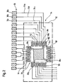
- FIG. 2 shows the printed pattern section 34 in detail.
- Pads 38a, 38b, ... are formed at the other ends of the printed patterns 34a, 34b, ... and collectively called a pad section 38.
- the pad section 38 shown in Figure 2 is called a QFP pattern on which QFPs (thin, square quad flat packages) are mounted.
- QFPs thin, square quad flat packages
- the pitch at which the pads 38a, 38b, ... are arranged is very small.
- the pad 38b and the pads 38x, 38y, and 38z are connected together by the printed pattern 34x to form a ground line.
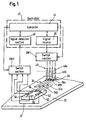
- the bare-board tester includes probes 40a, 40b, ... that are a plurality of first terminals connected to the pads 36a, 36b, ... on the circuit board 32.
- the plurality of probes 40a, 40b, ... are collectively called a probe section 40.
- FIG. 7A schematically shows the switch section SW1.
- the switch section SW1 includes a plurality of switches SW1a, SW1b, ... Each switch is turned on/off in response to an instruction from a computer 44 to transmit a signal provided by the signal source 46 to a desired probe in the probe section 40, for example, the probe 40a, as shown in Figure 1 (in this case, only the switch SW1a is turned on).
- the signal transmitted to the probe 40a is provided to the pad 38a (see Figure 2) of the pad section 38 via the pad 36a of the pad section 36 and the printed pattern 34a in the printed pattern section 34 which are connected to the probe 40a.
- a sensor module 50 is located on the pad section 38 on the circuit board 32.
- the sensor module 50 is coupled to the pad section 38 in order to obtain a signal from the pad section 38 and to supply it to a switch section SW2 that is a second switch means.
- the sensor module 50 comprises four integrally formed sensor units 52, 54, 56, and 58 as shown in Figure 2. Each sensor unit corresponds to a second terminal. According to this embodiment, the sensor module 50 is composed of a circuit board 60 (see Figure 4B) that is manufactured through a process similar to the inspected circuit board 32.
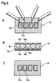
- Figures 4A, 4B, and 4C schematically shows the sensor unit 52 constituting part of the sensor module 50.
- the sensor unit 52 corresponds to the eight pads 38a, 38b, ... (these eight pads form one group) but is shown to correspond to four pads in Figures 4A, 4B, and 4C for case of understanding.
- Figure 4A is a plan view of the sensor unit 52.
- Figure 4B is a cross sectional view showing an integral part.
- Figure 4C is a bottom view.
- electrode plates 62a, 62b, ... constituting an electrode section are independently provided on the bottom surface of the circuit board 60.
- An insulating film 70 is formed to cover the electrode plates 62a, 62b, ... .
- the electrode plates 62a, 62b, ... are located opposite to the pads 38a, 38b, ... (see Figure 2) of the pad section 38 of the inspected circuit board 32 that corresponds to the sensor unit 52 in order to form a group.
- the electrode plate is formed to have almost the same shape as each pad.
- the electrode 62a and insulating film 70 of the sensor unit 52 join the pad 38a of the inspected circuit board 32 to form a capacitor. This is true of the other electrode plates 62b, ... .
- connection plate 64 that serves as a connection conducting section is provided on the top surface of the circuit board 60.
- the connection plate 64 is electrically connected to the electrode plates 62a, 62b, ... via through-holes 66a, 66b, ...
- the connection plate 64 of the sensor unit 52 is capacitively coupled to the group of pads 38a, 38b, ... described above.
- the connection plate 64 is connected to the switch section SW2 via a connection cord 72.
- the connection plate 64 and the through-holes 66a, 66b, ... correspond to a connection means.
- shield films 68a and 68b that are shield members are formed on the bottom and top surfaces of the circuit board 60, and connected to each other via a through-hole 68c.
- a ground potential is applied to the shield films 68a and 68b.
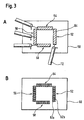
- Figure 3A shows a plan view of the sensor module 50.
- Figure 3B is a perspective view of the bottom surface of the sensor module 50 as seen from above.
- FIG 7B schematically shows the switch section SW2.
- the switch section SW2 comprises four switches SW2a, SW2b, SW2c, and SW2d. Each switch is turned on/off in response to an instruction from the computer 44 (see Figure 1) to supply a signal detection section with a signal from a desired one of the four sensor units 52, 54, 56, and 58 constituting the sensor module 50, for example the sensor unit 52 (in this case, only the switch SW2a is turned on).
- the signal provided by the desired sensor unit 52 is subjected to a predetermined process in the detection section 48 and then delivered to the computer 44, as shown in Figure 1. Based on the transmitted signal, the computer 44 determines the continuity of a printed pattern selected by the switch sections SW1 and SW2 (in the above example, the printed pattern 34a).
- the computer 44, the signal source 46, and the signal detection section 48 constitute a controller 42.
- the sensor module 50 of the four sensor units 52, 54, 56, and 58 By designing the sensor module 50 of the four sensor units 52, 54, 56, and 58 so that a signal can be independently obtained from each sensor unit in this manner, the following advantages can be obtained.
- the pad section 38 (the QFP pattern) of the printed pattern section 34 shown in Figure 2 the pad 38b and the pads 38x, 38y, and 38z are connected together by the printed pattern 34x to form a ground line.
- a single large electrode plate 62 may be provided on the bottom surface of the circuit board 60 as shown in Figures 5A, 5B, and 5C. That is, the single large electrode plate 62 of the sensor unit 52 is coupled to the group of pads 38a, 38b, ... (see Figure 2) corresponding to the sensor unit 52.
- This configuration is advantageous because the variation in the electrostatic capacity generated between the electrode plate 62 and the group of pads 38a, 38b, ... shown in Figure 2 is relatively small even if these components are only roughly aligned with each other.
- the above embodiment connects the plurality of electrode plates 62a, 62b,... to the single connection plate 64 to allow all the plurality of pads 38a, 38b, ... corresponding to the sensor unit 52 shown in Figure 2 to be subjected to a single signal processing, as shown in Figures 4B and 4A.
- a plurality of connection plates 64a, 64b, ... may be provided on the top surface of the circuit board 60 and connected to the electrode plates 62a, 62b, ..., respectively, via the through-holes 66a, 66b, ... to obtain a signal from the connection plates 64a, 64b, ..., as shown in Figure 6A, 6B, and 6C.
- the plurality of pads 38a, 38b, ... shown in Figure 2 can be individually subjected to signal processing. This enables more delicate processing to allow the apparatus to inspect more complicated printed patterns.
- the pads 38a, 38b, ... form individual group. That is, each group is composed of only a single pad.
- the above embodiment integrates the four sensor units 52, 54, 56, and 58 into the sensor module 50, these sensor units may be separately formed.
- the integration allows the plurality of sensor units to be handled easily compared to the separation of the units.
- the integral sensor module 50 can be more efficiently positioned on the circuit board 32.
- Figure 9 is a timing chart showing signal processing.
- the signal processing executed by the bare-board tester will be described with reference to Figures 18 and 9.
- Figure 9 omits the description of a few switches that constitute the switch sections SW1 and SW2.
- This embodiment uses a constant voltage source as the signal source 46 (see (a) in Figure 9).
- a constant voltage E is applied to the switch SW1 by the signal source 46, as shown in Figure 1.
- the computer 44 first transmits an instruction to the switch section SW2 to turn on only the switch SW2a while turning the other switches SW2b, SW2c, and SW2d off (see Figures 7B and (b) in Figure 9). Then, only the sensor unit 52 is connected to the signal detection circuit 48, whereas the other sensor units 54, 56, and 58 remain disconnected from the signal detection 48.
- the computer 44 then sends an instruction to the switch SW1 to turn on the switch SW1a (see (c) in Figure 9) while turning the other switches SW1b, SW1c, ... off (see Figure 7A). Then, only the probe 40a is connected to the signal source 46, whereas the probes 40b, 40c, ... remain disconnected from the signal source 46. This causes the printed pattern 34a on the circuit board 32 to be selected and inspected.
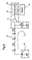
- a resistor R1 represents the internal resistance of the switches SW1a and SW2a
- a resistor R2 represents the resistance of the printed pattern 34a on the circuit board 32.
- a resistor R3 represents the ground resistance in the signal detection section 48.
- a capacitor C1 represents a capacitor formed of the electrode plates 62a, 62b, ... of the sensor unit 52, the insulating film 70 (see Figure 4B), and the pads 38a, 38b, ... corresponding to the sensor unit 52.
- E represents a direct voltage from the signal source 46.
- a peak hold circuit 76 detects and stores its maximum value (corresponding to the voltage Va in (d) in Figure 9).
- the peak hold circuit 76 includes a D/A converter (not shown) that digitalizes and transmits the maximum value to the computer 44. Part of the function of the peak hold circuit 76 can be implemented by the computer 44.
- the computer 44 determines the continuity of the printed pattern 34a on the circuit board 32. For example, it makes a determination by checking whether the maximum value is between the prescribed upper and lower reference limits.
- the peak hold circuit 76 can detect the maximum value in a very short time, which enables the continuity of the printed pattern to also be determined in a very short time. As a result, the operation is unlikely to be affected by noise.
- the computer 44 then transmits an instruction to the switch SW1 to turn on the switch SW1b (see (e) in Figure 9).
- the switch SW1a remains on.
- the probes 40a and 40b are connected to the signal source 46.
- the condition of the switch section SW2 remains unchanged.
- the voltage Vx input to the amplifier 74 exhibits a maximum value Vb (see (f) in Figure 9) almost simultaneously with the activation of the switch SW1b (see (e) in Figure 9).
- the computer 44 determines the continuity of the printed pattern 34b on the circuit board 32 based on the maximum value Vb, as described above.
- the sensor module 50 is composed of the plurality of sensor units 52, 53, ... (see Figure 2), each of which is coupled to the corresponding group of pads via the separate capacitor.
- the electrostatic capacity of each capacitor C1 is relatively small. That is, a shown in Equation (1) has a relatively large value (that is, the time constant correspondingly has a small value).
- the time (t) required until the current (i) falls close to zero is short, as is apparent from Equation (1).
- This embodiment can thus determine the continuity of the printed patterns in short cycles.
- the computer 44 then activates of the switch sections SW1 and SW2 as required to inspect the continuity of the printed patterns 34c, ... If the circuit board 32 is acceptable as shown in Figure 9, that is, if the printed patterns 34a, 34b, 34c, ... are not open-circuited, the voltage Vx input to the amplifier 74 is as shown in (d), (f), (g),..., respectively.
- This embodiment can thus inspect the continuity of the printed pattern promptly and accurately.
- the switch SW1a may be turned off immediately after the peak hold circuit 76 has detected the maximum value for the printed pattern 34a (the maximum value corresponding to the voltage Va), followed by the turn-on of the switch SW1b.
- This configuration eliminates the need to wait for the current (i) flowing through the printed pattern 34a to fall close to zero before starting the inspection of the next printed pattern 34b.
- the continuity of the printed patterns can be inspected in shorter cycles.
- This configuration also prevents the length of the inspection cycle from being increased drastically even if the time constant (an inverse of ⁇ in Equations (1) and (2)) is large.
- the above embodiment uses the constant-voltage source as the signal source 46 (see (a) in Figure 9) and turns each switch of the switch section SW1 on/off (see (c) and (e) in Figure 9) to obtain a voltage with waveform-shaped steps and having sharp rising edges, a circuit that sequentially generates signals with rapid changes may be used as the signal source 46.
- Figure 10 shows a timing chart of signal processing executed when the signal source 46 described above is used.
- This example employs a rectangular-wave generating circuit as the signal source 46.
- the computer 44 distributes among the printed patterns 34a, 34b, ... each rectangular signal sequentially generated by the signal source 46 ( Figure 11).
- the condition of the voltage Vx input to the amplifier 74 and the processing executed after it has been input to the amplifier 74 are similar to those in the example shown in Figure 9.
- the signal source 46 may be configured to generate triangular waves as shown in Figure 11A.
- each triangular wave has sharp rising edges (a).
- the signal source 46 may be configured to generate a pulse train as shown in Figure 11B.
- each pulse signal has sharp rising edges (b), as in Figure 11A.
- the signal having sharp rising edges is not limited to the ones described above. It includes not only those rising at time 0 but also those delaying rising. It also includes those having sharp falling edges.
- this invention determines the continuity of the wiring based on the maximum voltage generated at the second terminal after the signal has changed rapidly, this invention is not limited to this aspect.
- This invention may be configured to determine the continuity of the wiring based on a quantity relating to the voltage generated between the first and the second terminals when a signal with rapid changes are applied, such as the average of the voltage within a specified period of time, the voltage value obtained after a specified period of time, the steady-state deviation voltage, or the maximum, average, or integral value of the current flowing between the first and second terminals, all values obtained after the signal has changed rapidly.
- the continuity of the wiring can be determined in a shorter time by using the maximum voltage as in the above embodiment.
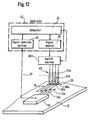
- Figure 12 shows the configuration of a bare-board tester that uses a sensor module 90 composed of a single second terminal.
- the configurations of the controller 42, the switch section SW1, and the probe section ⁇ 40 are similar to those in the bare-board tester shown in Figure 1.
- the bare-board tester shown in Figure 12 has only one output from the sensor module 90. Thus, it does not include the switch SW2 that switches the output from the sensor module 50 to supply it to the signal detection section 48, as in Figure 1.
- the sensor module 90 disposed on the pad section 38 (see Figure 2) of the circuit board 32 is coupled to the pad section 38 to obtain a signal therefrom in order to deliver directly it to the signal detection section 48.
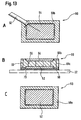
- Figures 13A, 13B, and 13C show the configuration of the sensor module 90.
- the sensor module 90 is composed of a circuit board 60 (see Figure 13B) manufactured through a process similar to that for the inspected circuit board 32 as in the above embodiment.
- Figure 13A is a plan view of the sensor module 90.
- Figure 13B is a cross sectional view of the integral part of the module.
- Figure 13C is a bottom view.
- one electrode plate 62 that is the electrode section is provided on the bottom surface of the circuit board 60, with an insulating film 70 formed to cover the electrode plate 62.
- the electrode plate 62 is disposed opposite to the pad section 38 of the inspected circuit board 32 and is capacitively coupled to all the pads 38a, 38b, ... (see Figure 2) in the pad section 38 via the insulating film 70.
- connection plate 64 is provided on the top surface of the circuit board 60, as shown in Figures 13A and 13B.
- the connection hole 64 is electrically connected to the electrode plate 62 via a through-hole 66.
- the connection plate 64 is connected to the signal detection section 48 via a connection cord 92.
- shield films 68a and 68b which are shield members, are formed on the bottom and the top surfaces of the circuit board 60, respectively, and connected to each other via a through-hole 68c.
- the shield films 68a and 68b are provided with a ground potential.
- the signal processing executed by the bare-board tester shown in Figure 12 is almost the same as that by the bare-board tester shown in Figure 1.
- the bare-board tester shown in Figure 12 does not execute processing for the switch section SW2, as described above.
- Part or all of the function of the computer 44 shown in Figure 1 or Figure 12 can also be implemented by hardware logic.
- part or all of the function of the signal source 46 or the signal detection section 48 can also be implemented by the computer.
- the shield members may be eliminated.
- the use of the shield members can reduce noise.
- the above embodiment provides the insulating film on the second terminal covering the electrode section, the insulating film may be eliminated. Providing the insulating film on the second terminal, can facilitate prompt inspections because it there is no need to prepare separate insulating films prior to inspection.
- connection conducting section on the other side may be eliminated.
- the structure of the sensor module can be simplified because a signal can be transmitted easily via this section.
- the sensor module is composed of the circuit board that is manufactured through a process similar to that used for the inspected circuit board, it may be made of a circuit board that is manufactured through a process dissimilar to that used for the inspected circuit board or may be configured without a circuit board.
- the sensor module By manufacturing the sensor module through a process similar to that used for the inspected circuit board, however, if the density or complicatedness of the wiring on the inspected circuit board has been increased, the density or complicatedness of the sensor module can be conveniently increased accordingly.
- the second terminal is capacitively coupled to the other end of the wiring.
- the capacitive coupling enables reliable inspections to be conducted using a simple configuration.
- the above embodiment provides the plurality of first terminals and uses the first switch means to select a desired first terminal in order to select one of the one ends of the wiring on the inspected circuit board.
- This configuration eliminates the need to move the inspected circuit board relative to the first terminal, thereby enabling inspections to be conducted very accurately, reducing the manufacturing cost of the apparatus, and allowing simple automation of inspections.
- this invention is not limited to such a tester.
- This invention is also applicable to general circuit board inspection apparatuses and methods such as those for inspecting a circuit board on which circuit elements such as a CPU are mounted or a package on which circuit elements are mounted.
Landscapes
- Engineering & Computer Science (AREA)
- Computer Hardware Design (AREA)
- Microelectronics & Electronic Packaging (AREA)
- General Engineering & Computer Science (AREA)
- Physics & Mathematics (AREA)
- General Physics & Mathematics (AREA)
- Testing Of Short-Circuits, Discontinuities, Leakage, Or Incorrect Line Connections (AREA)
- Tests Of Electronic Circuits (AREA)
- Measuring Leads Or Probes (AREA)
Claims (7)
- Un appareil d'inspection de carte de circuit pour inspecter des pistes (34a, 34b, ...) formées sur une carte de circuit (32), comprenant :caractérisé en ce queune multiplicité de premières bornes (40a, 40b, ...) destinées à être respectivement en contact et en connexion électrique avec des extrémités (36a, 36b, ...) de ces pistes,un dispositif d'application de signal (46, SW1) pour appliquer sélectivement à chacune des premières bornes un signal de test prédéterminé,une seconde borne (52, 54, 56, 58) qui est destinée à faire face, avec un espace, aux autres extrémités des pistes, en couplage capacitif avec celles-ci, afin de recevoir le signal de test transmis par le couplage capacitif, etun détecteur (48) pour détecter la continuité de la piste qui reçoit le signal de test,
le signal de test appliqué aux premières bornes (40a, 40b, ...) a un front montant ou descendant abrupt, et
le détecteur est adapté pour détecter la continuité des pistes conformément à la valeur maximale du signal de test reçu par la seconde borne (52, 54, 56, 58), cette valeur maximale étant associée au front montant ou descendant. - Un appareil d'inspection de carte de circuit selon la revendication 1, caractérisé en ce que le dispositif d'application de signal comprend une source de tension constante (46) et un commutateur (SW1) pour connecter sélectivement la source de tension (46) à l'une des premières bornes (40a, 40b, ...), le front montant ou descendant abrupt étant généré au moment de la commutation du commutateur (SW1).
- Un appareil d'inspection de carte de circuit selon la revendication 1, caractérisé en ce que le dispositif d'application de signal comprend un générateur pour générer un signal de forme d'onde rectangulaire.
- Un appareil d'inspection de carte de circuit selon l'une quelconque des revendications 1 à 3, caractérisé par un circuit de blocage de valeur de crête (76) pour bloquer la valeur maximale du signal de test reçu par la seconde borne.
- Un appareil d'inspection de carte de circuit selon l'une quelconque des revendications 1 à 4, caractérisé par une pellicule électriquement isolante (70) interposée entre la seconde borne et la carte de circuit à inspecter.
- Un appareil d'inspection de carte de circuit selon l'une quelconque des revendications 1 à 5, caractérisé par un élément de blindage placé autour de la seconde borne.
- Un appareil d'inspection de carte de circuit selon l'une quelconque des revendications 1 à 6, caractérisé par une multiplicité de secondes bornes (52, 54, 56, 58), chacune d'elles faisant face à une multiplicité d'extrémités de pistes, et étant en couplage capacitif avec celles-ci.
Applications Claiming Priority (3)
| Application Number | Priority Date | Filing Date | Title |
|---|---|---|---|
| JP4612797 | 1997-02-28 | ||
| JP46127/97 | 1997-02-28 | ||
| JP04612797A JP3165056B2 (ja) | 1997-02-28 | 1997-02-28 | 基板検査装置および基板検査方法 |
Publications (3)
| Publication Number | Publication Date |
|---|---|
| EP0862061A2 EP0862061A2 (fr) | 1998-09-02 |
| EP0862061A3 EP0862061A3 (fr) | 2000-02-02 |
| EP0862061B1 true EP0862061B1 (fr) | 2003-01-15 |
Family
ID=12738329
Family Applications (1)
| Application Number | Title | Priority Date | Filing Date |
|---|---|---|---|
| EP98103453A Expired - Lifetime EP0862061B1 (fr) | 1997-02-28 | 1998-02-27 | Procédé et dispositif de contrôle de cartes de circuit |
Country Status (4)
| Country | Link |
|---|---|
| US (1) | US5969530A (fr) |
| EP (1) | EP0862061B1 (fr) |
| JP (1) | JP3165056B2 (fr) |
| DE (1) | DE69810681T2 (fr) |
Families Citing this family (24)
| Publication number | Priority date | Publication date | Assignee | Title |
|---|---|---|---|---|
| US6316949B1 (en) | 1999-01-19 | 2001-11-13 | Nidec-Read Corporation | Apparatus and method for testing electric conductivity of circuit path ways on circuit board |
| JP2001194405A (ja) * | 2000-01-07 | 2001-07-19 | Oht Kk | 基板検査用プローブおよび基板検査方法 |
| US7049826B2 (en) * | 2000-09-11 | 2006-05-23 | Oht Inc. | Inspection device and inspection method |
| JP2002156417A (ja) * | 2000-11-17 | 2002-05-31 | Oht Inc | 回路基板の検査装置及び検査方法 |
| JP2002156399A (ja) * | 2000-11-17 | 2002-05-31 | Oht Inc | 回路基板の検査装置及び検査方法 |
| WO2002086520A1 (fr) * | 2001-04-19 | 2002-10-31 | Oht Inc. | Appareil d'inspection et procede d'inspection |
| US7250781B2 (en) * | 2002-12-19 | 2007-07-31 | Fuji Xerox Co., Ltd. | Circuit board inspection device |
| KR100593647B1 (ko) * | 2004-05-18 | 2006-06-28 | 삼성전자주식회사 | 프로브 센싱용 패드, 반도체 소자가 탑재된 기판 및 반도체 소자 검사 방법 |
| KR100739629B1 (ko) * | 2005-12-02 | 2007-07-16 | 삼성전자주식회사 | 프로브 센싱용 패드 및 이를 이용한 프로브 니들 접촉 위치검사 방법. |
| DE102005022884B4 (de) * | 2005-05-18 | 2011-08-18 | Siemens AG, 80333 | Verfahren zur Inspektion einer Leiterbahnstruktur |
| US20080061812A1 (en) * | 2006-09-13 | 2008-03-13 | Sun Microsystems, Inc. | Component-attach test vehicle |
| US7439751B2 (en) * | 2006-09-27 | 2008-10-21 | Taiwan Semiconductor Manufacturing Co, Ltd. | Apparatus and method for testing conductive bumps |
| US7855567B2 (en) * | 2008-04-01 | 2010-12-21 | Test Research, Inc. | Electronic device testing system and method |
| IT1402434B1 (it) * | 2010-06-10 | 2013-09-04 | St Microelectronics Srl | Struttura di rilevamento dell'allineamento di una sonda atta a testare circuiti integrati |
| KR101149759B1 (ko) * | 2011-03-14 | 2012-06-01 | 리노공업주식회사 | 반도체 디바이스의 검사장치 |
| JP6221358B2 (ja) * | 2013-06-04 | 2017-11-01 | 日本電産リード株式会社 | 基板検査方法、及び基板検査装置 |
| TWI531803B (zh) * | 2013-12-17 | 2016-05-01 | 致伸科技股份有限公司 | 電路板之測試系統 |
| TWI500945B (zh) * | 2013-12-17 | 2015-09-21 | Primax Electronics Ltd | 電路板之測試系統 |
| JP6095735B2 (ja) * | 2014-07-29 | 2017-03-15 | ヤマハファインテック株式会社 | プリント基板検査装置及び検査方法 |
| TWI634339B (zh) * | 2017-11-21 | 2018-09-01 | 興城科技股份有限公司 | 檢測薄膜電晶體基板之方法及裝置 |
| US10641818B2 (en) * | 2018-08-27 | 2020-05-05 | Keysight Technologies, Inc. | Shape conformable capacitive coupler |
| US11879935B2 (en) * | 2020-09-25 | 2024-01-23 | Nokomis, Inc. | Testing of microelectronics device and method |
| JP7581868B2 (ja) * | 2020-12-25 | 2024-11-13 | 株式会社プロテリアル | 多心ケーブルの検査装置及び多心ケーブルの検査方法 |
| DE102025111898A1 (de) * | 2024-04-30 | 2025-10-30 | Sew-Eurodrive Gmbh & Co Kg | Verfahren und System zum Prüfen einer mit Bauteilen bestückten Leiterplatte mit einem Nadeladapter |
Citations (1)
| Publication number | Priority date | Publication date | Assignee | Title |
|---|---|---|---|---|
| JPH03154879A (ja) * | 1989-11-10 | 1991-07-02 | Nec Corp | 基板検査装置 |
Family Cites Families (16)
| Publication number | Priority date | Publication date | Assignee | Title |
|---|---|---|---|---|
| US5138266A (en) * | 1989-10-20 | 1992-08-11 | Digital Equipment Corporation | Single-probe charge measurement testing method |
| JPH04244976A (ja) * | 1991-01-31 | 1992-09-01 | Sony Chem Corp | コネクタの導通検査方法 |
| US5469064A (en) * | 1992-01-14 | 1995-11-21 | Hewlett-Packard Company | Electrical assembly testing using robotic positioning of probes |
| US5274336A (en) * | 1992-01-14 | 1993-12-28 | Hewlett-Packard Company | Capacitively-coupled test probe |
| US5696451A (en) * | 1992-03-10 | 1997-12-09 | Hewlett-Packard Co. | Identification of pin-open faults by capacitive coupling |
| US5266901A (en) * | 1992-05-29 | 1993-11-30 | International Business Machines Corp. | Apparatus and method for resistive detection and waveform analysis of interconenction networks |
| US5359291A (en) * | 1993-04-01 | 1994-10-25 | Alliedsignal Inc. | Method and apparatus for detecting short circuits |
| IT1261074B (it) * | 1993-07-05 | 1996-05-08 | Luciano Bonaria | Metodo e dispositivo di collaudo per schede elettroniche |
| US5426372A (en) * | 1993-07-30 | 1995-06-20 | Genrad, Inc. | Probe for capacitive open-circuit tests |
| JPH07146323A (ja) * | 1993-11-22 | 1995-06-06 | Inter Tec:Kk | 液晶表示器用ガラス基板の検査方法及び検査装置 |
| JP3228631B2 (ja) * | 1993-12-24 | 2001-11-12 | 東京エレクトロン株式会社 | テスタ |
| JP3617013B2 (ja) * | 1994-08-15 | 2005-02-02 | オー・エイチ・ティー株式会社 | 電子回路基板の検査装置及び電子回路の検査方法 |
| US5747999A (en) * | 1994-08-15 | 1998-05-05 | Okano Hitech Co., Ltd. | Feed control element used in substrate inspection and method and apparatus for inspecting substrates |
| JP3558434B2 (ja) * | 1995-11-30 | 2004-08-25 | 富士通オートメーション株式会社 | 電気的配線検査方法及び装置 |
| US5570027A (en) * | 1995-04-19 | 1996-10-29 | Photocircuits Corporation | Printed circuit board test apparatus and method |
| US5736862A (en) * | 1995-06-22 | 1998-04-07 | Genrad, Inc. | System for detecting faults in connections between integrated circuits and circuit board traces |
-
1997
- 1997-02-28 JP JP04612797A patent/JP3165056B2/ja not_active Expired - Lifetime
-
1998
- 1998-02-27 DE DE69810681T patent/DE69810681T2/de not_active Expired - Fee Related
- 1998-02-27 US US09/032,147 patent/US5969530A/en not_active Expired - Lifetime
- 1998-02-27 EP EP98103453A patent/EP0862061B1/fr not_active Expired - Lifetime
Patent Citations (1)
| Publication number | Priority date | Publication date | Assignee | Title |
|---|---|---|---|---|
| JPH03154879A (ja) * | 1989-11-10 | 1991-07-02 | Nec Corp | 基板検査装置 |
Also Published As
| Publication number | Publication date |
|---|---|
| JPH10239372A (ja) | 1998-09-11 |
| DE69810681T2 (de) | 2003-08-14 |
| DE69810681D1 (de) | 2003-02-20 |
| EP0862061A3 (fr) | 2000-02-02 |
| US5969530A (en) | 1999-10-19 |
| EP0862061A2 (fr) | 1998-09-02 |
| JP3165056B2 (ja) | 2001-05-14 |
Similar Documents
| Publication | Publication Date | Title |
|---|---|---|
| EP0862061B1 (fr) | Procédé et dispositif de contrôle de cartes de circuit | |
| EP0862062B1 (fr) | Procédé et dispositif de contrôle de cartes de circuit | |
| US5517110A (en) | Contactless test method and system for testing printed circuit boards | |
| US5469064A (en) | Electrical assembly testing using robotic positioning of probes | |
| JPH06213955A (ja) | テストプローブ | |
| US5625292A (en) | System for measuring the integrity of an electrical contact | |
| US6462556B2 (en) | Circuit board testing apparatus and method | |
| JPH09264919A (ja) | 基板検査方法及び装置 | |
| US6734681B2 (en) | Apparatus and methods for testing circuit boards | |
| US6798212B2 (en) | Time domain reflectometer probe having a built-in reference ground point | |
| US6353327B2 (en) | Circuit board misalignment detection apparatus and method | |
| JP3361311B2 (ja) | 基板検査装置および基板検査方法 | |
| JPH11153638A (ja) | 基板検査装置および基板検査方法 | |
| JP4200182B2 (ja) | 回路基板検査装置 | |
| JP2000074975A (ja) | 基板検査装置および基板検査方法 | |
| JPH11133090A (ja) | 基板検査装置および基板検査方法 | |
| JPS62269075A (ja) | プリント基板検査装置 | |
| JP4292013B2 (ja) | 回路基板検査装置 | |
| JP2004144759A (ja) | 検査装置及び検査方法 | |
| JPH1194896A (ja) | 半導体試験装置用布線インターフェイス検査装置 | |
| JP2004144760A (ja) | 検査装置及び検査方法 | |
| JPH05133992A (ja) | 回路基板検査方法と検査基板並びに回路基板検査装置 | |
| JP2004085584A (ja) | 検査装置及び検査方法 | |
| JPH03120484A (ja) | 集積回路検査装置 | |
| JPH03244142A (ja) | 半導体デバイスの検査方法 |
Legal Events
| Date | Code | Title | Description |
|---|---|---|---|
| PUAI | Public reference made under article 153(3) epc to a published international application that has entered the european phase |
Free format text: ORIGINAL CODE: 0009012 |
|
| AK | Designated contracting states |
Kind code of ref document: A2 Designated state(s): DE FR GB |
|
| AX | Request for extension of the european patent |
Free format text: AL;LT;LV;MK;RO;SI |
|
| PUAL | Search report despatched |
Free format text: ORIGINAL CODE: 0009013 |
|
| AK | Designated contracting states |
Kind code of ref document: A3 Designated state(s): AT BE CH DE DK ES FI FR GB GR IE IT LI LU MC NL PT SE |
|
| AX | Request for extension of the european patent |
Free format text: AL;LT;LV;MK;RO;SI |
|
| RIC1 | Information provided on ipc code assigned before grant |
Free format text: 7G 01R 31/312 A, 7G 01R 31/28 B |
|
| 17P | Request for examination filed |
Effective date: 20000717 |
|
| AKX | Designation fees paid |
Free format text: DE FR GB |
|
| 17Q | First examination report despatched |
Effective date: 20010810 |
|
| GRAH | Despatch of communication of intention to grant a patent |
Free format text: ORIGINAL CODE: EPIDOS IGRA |
|
| GRAH | Despatch of communication of intention to grant a patent |
Free format text: ORIGINAL CODE: EPIDOS IGRA |
|
| GRAA | (expected) grant |
Free format text: ORIGINAL CODE: 0009210 |
|
| AK | Designated contracting states |
Kind code of ref document: B1 Designated state(s): DE FR GB |
|
| REG | Reference to a national code |
Ref country code: GB Ref legal event code: FG4D |
|
| REF | Corresponds to: |
Ref document number: 69810681 Country of ref document: DE Date of ref document: 20030220 Kind code of ref document: P |
|
| PGFP | Annual fee paid to national office [announced via postgrant information from national office to epo] |
Ref country code: GB Payment date: 20030704 Year of fee payment: 6 |
|
| PGFP | Annual fee paid to national office [announced via postgrant information from national office to epo] |
Ref country code: FR Payment date: 20030716 Year of fee payment: 6 |
|
| ET | Fr: translation filed | ||
| PLBE | No opposition filed within time limit |
Free format text: ORIGINAL CODE: 0009261 |
|
| STAA | Information on the status of an ep patent application or granted ep patent |
Free format text: STATUS: NO OPPOSITION FILED WITHIN TIME LIMIT |
|
| 26N | No opposition filed |
Effective date: 20031016 |
|
| PG25 | Lapsed in a contracting state [announced via postgrant information from national office to epo] |
Ref country code: GB Free format text: LAPSE BECAUSE OF NON-PAYMENT OF DUE FEES Effective date: 20040227 |
|
| GBPC | Gb: european patent ceased through non-payment of renewal fee | ||
| PG25 | Lapsed in a contracting state [announced via postgrant information from national office to epo] |
Ref country code: FR Free format text: LAPSE BECAUSE OF NON-PAYMENT OF DUE FEES Effective date: 20041029 |
|
| REG | Reference to a national code |
Ref country code: FR Ref legal event code: ST |
|
| PGFP | Annual fee paid to national office [announced via postgrant information from national office to epo] |
Ref country code: DE Payment date: 20070223 Year of fee payment: 10 |
|
| PG25 | Lapsed in a contracting state [announced via postgrant information from national office to epo] |
Ref country code: DE Free format text: LAPSE BECAUSE OF NON-PAYMENT OF DUE FEES Effective date: 20080902 |