EP0862182A1 - Löschverfahren für statischen RAM-Speicher und zugehörige Speicherschaltung - Google Patents
Löschverfahren für statischen RAM-Speicher und zugehörige Speicherschaltung Download PDFInfo
- Publication number
- EP0862182A1 EP0862182A1 EP98400465A EP98400465A EP0862182A1 EP 0862182 A1 EP0862182 A1 EP 0862182A1 EP 98400465 A EP98400465 A EP 98400465A EP 98400465 A EP98400465 A EP 98400465A EP 0862182 A1 EP0862182 A1 EP 0862182A1
- Authority
- EP
- European Patent Office
- Prior art keywords
- cells
- group
- static ram
- memory
- ram memory
- Prior art date
- Legal status (The legal status is an assumption and is not a legal conclusion. Google has not performed a legal analysis and makes no representation as to the accuracy of the status listed.)
- Granted
Links
- 230000015654 memory Effects 0.000 title claims abstract description 64
- 230000003068 static effect Effects 0.000 title claims abstract description 20
- 238000000034 method Methods 0.000 title claims description 7
- 230000001902 propagating effect Effects 0.000 claims abstract 2
- 238000012217 deletion Methods 0.000 claims description 4
- 230000037430 deletion Effects 0.000 claims description 4
- 238000005516 engineering process Methods 0.000 description 6
- 238000001514 detection method Methods 0.000 description 5
- 230000010287 polarization Effects 0.000 description 5
- 230000008520 organization Effects 0.000 description 4
- 230000000295 complement effect Effects 0.000 description 3
- 238000011144 upstream manufacturing Methods 0.000 description 3
- 230000004913 activation Effects 0.000 description 2
- 230000006870 function Effects 0.000 description 2
- 101710116852 Molybdenum cofactor sulfurase 1 Proteins 0.000 description 1
- 101710116850 Molybdenum cofactor sulfurase 2 Proteins 0.000 description 1
- 230000003213 activating effect Effects 0.000 description 1
- 239000006185 dispersion Substances 0.000 description 1
- 238000002474 experimental method Methods 0.000 description 1
- 239000000463 material Substances 0.000 description 1
- 239000011159 matrix material Substances 0.000 description 1
- 238000002161 passivation Methods 0.000 description 1
- 238000012545 processing Methods 0.000 description 1
- 238000011084 recovery Methods 0.000 description 1
- 230000000630 rising effect Effects 0.000 description 1
- 230000007480 spreading Effects 0.000 description 1
- 238000012360 testing method Methods 0.000 description 1
- 238000011282 treatment Methods 0.000 description 1
- 230000001960 triggered effect Effects 0.000 description 1
Images


Classifications
-
- G—PHYSICS
- G11—INFORMATION STORAGE
- G11C—STATIC STORES
- G11C11/00—Digital stores characterised by the use of particular electric or magnetic storage elements; Storage elements therefor
- G11C11/21—Digital stores characterised by the use of particular electric or magnetic storage elements; Storage elements therefor using electric elements
- G11C11/34—Digital stores characterised by the use of particular electric or magnetic storage elements; Storage elements therefor using electric elements using semiconductor devices
- G11C11/40—Digital stores characterised by the use of particular electric or magnetic storage elements; Storage elements therefor using electric elements using semiconductor devices using transistors
- G11C11/41—Digital stores characterised by the use of particular electric or magnetic storage elements; Storage elements therefor using electric elements using semiconductor devices using transistors forming static cells with positive feedback, i.e. cells not needing refreshing or charge regeneration, e.g. bistable multivibrator or Schmitt trigger
- G11C11/413—Auxiliary circuits, e.g. for addressing, decoding, driving, writing, sensing, timing or power reduction
- G11C11/417—Auxiliary circuits, e.g. for addressing, decoding, driving, writing, sensing, timing or power reduction for memory cells of the field-effect type
- G11C11/419—Read-write [R-W] circuits
-
- G—PHYSICS
- G11—INFORMATION STORAGE
- G11C—STATIC STORES
- G11C7/00—Arrangements for writing information into, or reading information out from, a digital store
- G11C7/10—Input/output [I/O] data interface arrangements, e.g. I/O data control circuits, I/O data buffers
- G11C7/1015—Read-write modes for single port memories, i.e. having either a random port or a serial port
-
- G—PHYSICS
- G11—INFORMATION STORAGE
- G11C—STATIC STORES
- G11C7/00—Arrangements for writing information into, or reading information out from, a digital store
- G11C7/10—Input/output [I/O] data interface arrangements, e.g. I/O data control circuits, I/O data buffers
- G11C7/1048—Data bus control circuits, e.g. precharging, presetting, equalising
Definitions
- the present invention relates to a method of erasing a static RAM memory and a memory in corresponding integrated circuit.
- Static RAM memories are used in number of microprocessor applications, especially in data processing, to contain data on which we perform calculations or other treatments. They are thus used to contain temporarily data. When the power is turned off, they lose their content, unless they are associated with a backup energy source (batteries).
- Static RAM memories are used in particular in "smart card” type products for which knows the high level of security required. These memories allow in these products to apply the different encryption or other calculations on data confidential.
- this erasure is material and non-software, for maximum security. It is triggered automatically, without recourse possible, by the detection of identified events, such as the setting on the integrated circuit or the detection of a anomaly, ensuring maximum security of said circuit.
- Global erasure can be obtained by selecting all the memory cells and activating transistors which pull the output to the mass. But we understand that in practice consumption of current induced by such an erasure operation global is problematic. Indeed, a bit line of 128 static RAM memory cells can for example consume up to 25 milliamps in erasure. Multiplied by the number of bit lines in the memory, we can end up with an unacceptable consumption in practice, depending on the total memory capacity. Yes memory thus has a capacity of 2 Kbytes, it it would take about 2 amps to ensure erasure global, snapshot of memory. It's not feasible.
- the invention offers a sequential erase operation of the memory, obtained by dividing memory into groups of memory cells and by spreading so controlled a group-to-group erase signal. The deletion of a cell group is then activated when deleting a previous group of cells is finished. In this way we spread over time the current consumption.
- the size of the cell group depends on the organization of the memory plan, its capacity, and consumption that we can accept. From the choice of this dimension directly depends on time total erasing required, which should be the most low possible to limit the duration as much as possible during which data could still be read and retrieved.
- the smallest group that can be used easily is a bit line of the memory plane, or of the half-plan when the memory plan is organized in two half plans, all word lines being selected.
- the group can correspond to two or several bit lines from which one selects simultaneously delete all cells together.
- the controlled propagation of the erasure signal is ensured by a delay circuit, placed between each group of cells, and sized to provide delay corresponding to the erasure time of a group cells. In this way, the consumption of current is spread over the entire erasing time of Memory. At a given time, it is equal to erasure current of a single group of cells.
- Figure 1 shows a RAM memory cell static in CMOS technology. This cell includes classic way two looped reversers I1 and I2, to complementary transistors.
- the first inverter I1 thus comprises a P-type MOS 1 transistor in series with a transistor MOS 2 type N, including grids linked together form the input E1 of the inverter and whose drains connected together form the output S1 of the inverter I1.
- the second inverter I2 includes a MOS transistor 3 of type P and a MOS transistor 4 of type N, whose grids connected together form the input E2 of the reverser and whose drains connected together form the output S2 of the inverter I1.
- the output S1 of the first inverter is connected to the input E2 of the second inverter and forms the terminal Q of the memory cell.
- the S2 output of the second inverter is connected to input E1 of the first inverter and forms the / Q terminal of the memory cell.
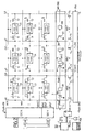
- FIG. 2 An example of RAM memory organization static is shown in figure 2. This is a matrix organization in bit lines (y0 to y7) and word lines (selx0 to selx127).
- Memory cells C1, C2 .. are shown diagrammatically by 2 looped reversers.
- a selection transistor T1 is connected between the terminal Q of each cell, for example C1 and the line associated bit, y0 in the example. This transistor selection is controlled on its grid by the signal of line selection of associated word selx0 in the example. When this selection signal is activated (in example, when it is "1"), all cells associated with this word line convey the level of their terminal Q on the associated bit line.
- each bit line and each additional bit line is connected to a circuit 5 for reading / writing by a transistor associated selection noted T3 for the bit line and T4 for the additional bit line. They are ordered on their grid by the line selection signal of corresponding bit, sely0 for lines y0 and / y0, sely1 for lines y1 and / y1, ..., sel y7 for lines y7 and / y7.
- the read / write circuit 5 is connected to the data input / output bus, D0-D7 and / D0- / D7 in The example.
- Word line and line selection signals bit lines are provided by respectively a word line decoder noted DEC-X and a decoder of bit lines noted DEC-Y. In normal operation, these decoders allow the selection of a word line and one or more bit lines, to read, write or delete an information word. We then find on the selected word line, (selx0 for example) the supply voltage Vdd of the circuit.
- the architecture represented is simple, but sufficient to explain the principle of the invention. Other common architectures are possible, especially those where the memory plan is divided in two half shots.
- the memory further comprises means 6 to erase all memory cells on activation of a flash-ON erase command signal generated internally.
- These means 6 for erasing comprise a transistor by group of cells to be deleted and delay circuits in series on a line of propagation of the flash-ON erase control signal, each of the delay circuits being placed between two groups of cells to be deleted.
- a group of cells corresponds to a bit line. Selecting a group of cells particular is then obtained by selecting the line corresponding bit, all word lines being previously selected.
- DEC-X word line decoder which allow this simultaneous global selection on activation of a signal control, which can be, for example, the signal erase flash-ON command.
- the DEC-X decoder can for example understanding logic circuits capable of impose an active state on all word lines when the flash-ON control signal is in the active state (1, in the example), the bus address signals address being ignored.
- an erase transistor connected between each bit line and ground, said transistor being controlled on its grid by the output of the delay circuit placed upstream of the bit.
- the erase transistor of the first line of bit y0 to clear, TE0 in the example can be directly controlled by the control signal erase flash-ON or by a delay circuit placed upstream, noted R0 in the example and represented by dotted in Figure 2.
- the other erase transistors, TE1 to TE7 in example, are respectively ordered on their grids by the flashl to flash7 outputs of the circuits retarders R1 to R7 each placed upstream of the corresponding erase transistor.
- each erase transistor is successively activated when the deletion of the group of previous cells is finished.
- the circuits retarders are sized to introduce a delay corresponding to the maximum time required for deleting the previous group. In practice we propagates the erasure signal of the first line of bit to the last, and possibly the first half plane on the second, to obtain the complete erasure of Memory.
- the cell groups are all equivalent (i.e. they have the same number of memory cells) and circuits retarders are all the same.
- the delay circuit R0 associated with the first group of cells (line y0) allows to have a structure identical for all cell groups. So we have same charge everywhere, which is preferable.
- the groups of cells according to the invention preferably include the same number of memory cells.
- the flash-ON signal could be a signal corresponding at least to the duration to delete a group of cells, with circuits retarders adapted to propagate without deformation this impulse.
- the delay circuits are sized for take into account variations due to temperature, the supply voltage or the dispersion of characteristics, so that the delay they induce either always greater than the erasure time of a group of cells.
- the flash-ON erase control signal is generated on detection of specific events. In practical, energizing the memory circuit or detection of anomalies by a circuit 8 for managing security sensors, leads to the generation of this flash-ON signal, as shown in figure 2.
- the flash-ON signal is generated from circuit 7 of energization of the memory circuit, which, on detection of a power supply rise (on the terminal Vcc) or reception of an alarm signal (ALARM) from sensor management circuit 8, generates a signal initialization POR of the memory circuit.
- This signal (or its inverse depending on its active level) is used to generate a pulse signal noted flash-RQ, applied on the input of setting to 1 (S) of a rocker RS.
- this flash-RQ signal has a rising pulse edge, output Q changes to one. This Q output is used as a flash-ON erase control signal.
- the flash-RQ signal brings it to its active level.
- the flash-END signal is applied to the input to reset the RS flip-flop to reset the flash-ON signal at its passive level.
- the scale can be reset by the POR initialization signal at power up.
- an OR gate is provided which receives in inputs POR and flash-END signals and whose output is applied to the reset input (R) of the rocking.
- Figure 3 details an example of circuit 6 of propagation of the flash-ON erase control signal and generating the end control signal erase flash-END.
- the propagation circuit 6 thus comprises a delay circuit per group of cells for propagate the flash-on erase command signal from group in group and a delay circuit extra after the last group of cells for generate the flash-END erase end signal.
- Each delay circuit includes in the example a first CMOS inverter with a first transistor P-type MOS T5 and a second MOS-type transistor N T6 whose grids connected together form the output, the source of transistor N being connected to the ground by an MOS transistor of the same N type T7, for impose a calibrated current in the branch, and delay so in a controlled manner the tilting of the inverter.
- the first inverter is followed by a second inverter to make the polarity of the input signal.
- T7 circuit load transistors retarders are biased by a single circuit polarization 9.
- this circuit of polarization 9 is a current mirror circuit activated by the flash-ON control signal. He understands an inverter 10 to control the grid of two P-type transistors T8 and T9 connected in series between the supply voltage and drain of a MOS transistor type N T10 having its gate connected to its drain, and its gate connected to the gate of each transistor of charge. The determined current flowing in the branch of polarization is thus copied in the branch of each delay circuit. This current is a function of characteristics of the circuit branch of polarization, that is, the geometries of the transistors and their type enriched or depleted.
- the circuit of polarization 10 is thus dimensioned according to the minimum delay we want to have between each group cells. It therefore depends on the characteristics of the memory cells considered.
- the delay circuit R0 for deleting the first group is not mandatory in principle. It allows to have an identity structure for all cell groups in the memory, which is preferably sought. But in circuits where we try to minimize the number of elements (space saving) or for which we are looking for the longest overall erasure time short as possible, it can be deleted.
- the R8 delay circuit for generating the end of erase command signal is valid for a flash-ON signal which remains active as long as one does not act to bring it back to its passive level. It is not necessary if you choose a flash-ON signal pulse type with a calibrated duration corresponding to the maximum erasure time of a group of cells, although this choice leads to a more complex propagation circuitry.
- the delay circuits use in the inverter a P-type transistor T5 for the switching low level to high level of the output, because under these conditions, such a transistor switches faster, which stops erasure as quickly as possible.
- the transistor erasure type N will have dimensions W / L of around 120 ⁇ / 0.7 ⁇ in CMOS technology at 0.7 ⁇ , for ability to pass a maximum current of 25 milliamps according to the experiments.
Landscapes
- Engineering & Computer Science (AREA)
- Microelectronics & Electronic Packaging (AREA)
- Computer Hardware Design (AREA)
- Read Only Memory (AREA)
- Static Random-Access Memory (AREA)
Applications Claiming Priority (2)
| Application Number | Priority Date | Filing Date | Title |
|---|---|---|---|
| FR9702454A FR2760286B1 (fr) | 1997-02-28 | 1997-02-28 | Procede d'effacement d'une memoire ram statique et memoire en circuit integre associe |
| FR9702454 | 1997-02-28 |
Publications (2)
| Publication Number | Publication Date |
|---|---|
| EP0862182A1 true EP0862182A1 (de) | 1998-09-02 |
| EP0862182B1 EP0862182B1 (de) | 1999-08-11 |
Family
ID=9504321
Family Applications (1)
| Application Number | Title | Priority Date | Filing Date |
|---|---|---|---|
| EP98400465A Expired - Lifetime EP0862182B1 (de) | 1997-02-28 | 1998-02-26 | Löschverfahren für statischen RAM-Speicher und zugehörige Speicherschaltung |
Country Status (4)
| Country | Link |
|---|---|
| US (1) | US6108232A (de) |
| EP (1) | EP0862182B1 (de) |
| DE (1) | DE69800015T2 (de) |
| FR (1) | FR2760286B1 (de) |
Families Citing this family (8)
| Publication number | Priority date | Publication date | Assignee | Title |
|---|---|---|---|---|
| JP2000019709A (ja) * | 1998-07-03 | 2000-01-21 | Hitachi Ltd | 半導体装置及びパターン形成方法 |
| US6772277B2 (en) * | 2001-04-30 | 2004-08-03 | Hewlett-Packard Development Company, L.P. | Method of writing to a memory array using clear enable and column clear signals |
| JP4713143B2 (ja) * | 2004-12-15 | 2011-06-29 | 富士通セミコンダクター株式会社 | 半導体記憶装置 |
| US8924626B2 (en) | 2010-04-29 | 2014-12-30 | Sandisk Technologies Inc. | Phased NAND power-on reset |
| US8458804B1 (en) * | 2011-12-29 | 2013-06-04 | Elwha Llc | Systems and methods for preventing data remanence in memory |
| WO2017138775A1 (ko) * | 2016-02-12 | 2017-08-17 | 한양대학교 산학협력단 | 메모리 장치 및 그 동작 방법 |
| CN113892137A (zh) * | 2021-03-30 | 2022-01-04 | 长江存储科技有限责任公司 | 存储器器件及其操作方法 |
| FR3128570B1 (fr) * | 2021-10-25 | 2023-10-27 | Commissariat Energie Atomique | Sram a initialisation reconfigurable |
Citations (2)
| Publication number | Priority date | Publication date | Assignee | Title |
|---|---|---|---|---|
| US4928266A (en) * | 1988-05-26 | 1990-05-22 | Visic, Inc. | Static ram with high speed, low power reset |
| EP0642131A2 (de) * | 1993-08-02 | 1995-03-08 | Nec Corporation | Statische RAM-Speicheranordnung mit Rücksetzschaltung |
Family Cites Families (4)
| Publication number | Priority date | Publication date | Assignee | Title |
|---|---|---|---|---|
| US4858182A (en) * | 1986-12-19 | 1989-08-15 | Texas Instruments Incorporated | High speed zero power reset circuit for CMOS memory cells |
| JPH0612612B2 (ja) * | 1987-03-06 | 1994-02-16 | 株式会社東芝 | 半導体記憶装置 |
| JPH01130385A (ja) * | 1987-11-17 | 1989-05-23 | Sony Corp | メモリ装置 |
| US5054000A (en) * | 1988-02-19 | 1991-10-01 | Sony Corporation | Static random access memory device having a high speed read-out and flash-clear functions |
-
1997
- 1997-02-28 FR FR9702454A patent/FR2760286B1/fr not_active Expired - Fee Related
-
1998
- 1998-02-26 EP EP98400465A patent/EP0862182B1/de not_active Expired - Lifetime
- 1998-02-26 DE DE69800015T patent/DE69800015T2/de not_active Expired - Lifetime
- 1998-02-27 US US09/032,630 patent/US6108232A/en not_active Expired - Lifetime
Patent Citations (2)
| Publication number | Priority date | Publication date | Assignee | Title |
|---|---|---|---|---|
| US4928266A (en) * | 1988-05-26 | 1990-05-22 | Visic, Inc. | Static ram with high speed, low power reset |
| EP0642131A2 (de) * | 1993-08-02 | 1995-03-08 | Nec Corporation | Statische RAM-Speicheranordnung mit Rücksetzschaltung |
Also Published As
| Publication number | Publication date |
|---|---|
| US6108232A (en) | 2000-08-22 |
| DE69800015T2 (de) | 2000-02-10 |
| FR2760286B1 (fr) | 1999-04-16 |
| FR2760286A1 (fr) | 1998-09-04 |
| DE69800015D1 (de) | 1999-09-16 |
| EP0862182B1 (de) | 1999-08-11 |
Similar Documents
| Publication | Publication Date | Title |
|---|---|---|
| FR2640798A1 (fr) | Dispositif de traitement de donnees comportant une memoire non volatile electriquement effacable et reprogrammable | |
| FR2667169A1 (fr) | Circuit de production de haute tension pour un circuit de memoire a semiconducteur. | |
| FR2715758A1 (fr) | Bascule bistable non volatile programmable par la source, notamment pour circuit de redondance de mémoire. | |
| EP1111621A1 (de) | Seitenprogrammierbar Flash-Speicher | |
| EP0862182B1 (de) | Löschverfahren für statischen RAM-Speicher und zugehörige Speicherschaltung | |
| FR2959580A1 (fr) | Circuit et procede de detection d'une attaque par injection de fautes | |
| EP1107259A1 (de) | Leseschaltung für integrierte Speicherschaltung | |
| FR2762434A1 (fr) | Circuit de lecture de memoire avec dispositif de limitation de precharge | |
| FR2665973A1 (fr) | Circuit d'optimisation d'effacement automatique pour une memoire a semiconducteur programmable et effacable electriquement et procede s'y rapportant. | |
| EP1900096A2 (de) | Widerstandsspeicherzelle | |
| FR2609831A1 (fr) | Circuit de lecture pour memoire | |
| EP4170655A1 (de) | Sram mit rekonfigurierbarer initialisierung | |
| EP0268513A1 (de) | Einrichtung zur Steuerung eines aus mehreren isolierbaren Segmenten bestehenden Bus | |
| EP0051525B1 (de) | Logische Anordnung mit vereinfachter elektrischer Programmierung | |
| FR2641391A1 (fr) | Composant logique programmable effacable rapide | |
| FR2801419A1 (fr) | Procede et dispositif de lecture pour memoire en circuit integre | |
| FR2771839A1 (fr) | Memoire non volatile programmable et effacable electriquement | |
| EP2073212B1 (de) | Lesevorrichtung eines nichtflüchtigen Speichers mit geringem Energieverbrauch und ihr Anwendungsverfahren | |
| FR3008534A1 (fr) | Procede de gestion du fonctionnement d'un dispositif de memoire associant un plan-memoire du type sram et un plan memoire du type non volatil, et dispositif de memoire correspondant | |
| EP0703584B1 (de) | Adressen-Dekodierverfahren für einen integrierten Speicher und Speicherschaltung zur Anwendung eines solchen Verfahrens | |
| FR2898223A1 (fr) | Circuit de distribution d'un signal initial a structure en arbre protege contre les aleas logiques. | |
| EP1417582A2 (de) | Schaltkreiskomplex mit dekontaminierungsmitteln für mit fehlern kontaminierte teile | |
| EP1630820A1 (de) | Speicherzellenprogrammierverfahren mit Detektion von Transkonduktanzdegradierung | |
| FR2828758A1 (fr) | Procede d'ecriture dans une memoire ram comportant un systeme d'effacement de colonnes | |
| EP0875899B1 (de) | Anordnung von zwei Speichern auf der selben monolitischen integrierten Schaltung |
Legal Events
| Date | Code | Title | Description |
|---|---|---|---|
| PUAI | Public reference made under article 153(3) epc to a published international application that has entered the european phase |
Free format text: ORIGINAL CODE: 0009012 |
|
| AK | Designated contracting states |
Kind code of ref document: A1 Designated state(s): DE FR GB IT |
|
| AX | Request for extension of the european patent |
Free format text: AL;LT;LV;MK;RO;SI |
|
| 17P | Request for examination filed |
Effective date: 19980813 |
|
| GRAG | Despatch of communication of intention to grant |
Free format text: ORIGINAL CODE: EPIDOS AGRA |
|
| GRAG | Despatch of communication of intention to grant |
Free format text: ORIGINAL CODE: EPIDOS AGRA |
|
| GRAH | Despatch of communication of intention to grant a patent |
Free format text: ORIGINAL CODE: EPIDOS IGRA |
|
| 17Q | First examination report despatched |
Effective date: 19981030 |
|
| RAP3 | Party data changed (applicant data changed or rights of an application transferred) |
Owner name: STMICROELECTRONICS S.A. |
|
| GRAH | Despatch of communication of intention to grant a patent |
Free format text: ORIGINAL CODE: EPIDOS IGRA |
|
| AKX | Designation fees paid |
Free format text: DE FR GB IT |
|
| RBV | Designated contracting states (corrected) |
Designated state(s): DE FR GB IT |
|
| GRAA | (expected) grant |
Free format text: ORIGINAL CODE: 0009210 |
|
| AK | Designated contracting states |
Kind code of ref document: B1 Designated state(s): DE FR GB IT |
|
| REF | Corresponds to: |
Ref document number: 69800015 Country of ref document: DE Date of ref document: 19990916 |
|
| GBT | Gb: translation of ep patent filed (gb section 77(6)(a)/1977) |
Effective date: 19990906 |
|
| ITF | It: translation for a ep patent filed | ||
| PLBE | No opposition filed within time limit |
Free format text: ORIGINAL CODE: 0009261 |
|
| STAA | Information on the status of an ep patent application or granted ep patent |
Free format text: STATUS: NO OPPOSITION FILED WITHIN TIME LIMIT |
|
| 26N | No opposition filed | ||
| REG | Reference to a national code |
Ref country code: GB Ref legal event code: IF02 |
|
| PGFP | Annual fee paid to national office [announced via postgrant information from national office to epo] |
Ref country code: IT Payment date: 20080213 Year of fee payment: 11 |
|
| PG25 | Lapsed in a contracting state [announced via postgrant information from national office to epo] |
Ref country code: IT Free format text: LAPSE BECAUSE OF NON-PAYMENT OF DUE FEES Effective date: 20090226 |
|
| PGFP | Annual fee paid to national office [announced via postgrant information from national office to epo] |
Ref country code: DE Payment date: 20110207 Year of fee payment: 14 Ref country code: FR Payment date: 20110311 Year of fee payment: 14 |
|
| PGFP | Annual fee paid to national office [announced via postgrant information from national office to epo] |
Ref country code: GB Payment date: 20110128 Year of fee payment: 14 |
|
| GBPC | Gb: european patent ceased through non-payment of renewal fee |
Effective date: 20120226 |
|
| REG | Reference to a national code |
Ref country code: FR Ref legal event code: ST Effective date: 20121031 |
|
| REG | Reference to a national code |
Ref country code: DE Ref legal event code: R119 Ref document number: 69800015 Country of ref document: DE Effective date: 20120901 |
|
| PG25 | Lapsed in a contracting state [announced via postgrant information from national office to epo] |
Ref country code: FR Free format text: LAPSE BECAUSE OF NON-PAYMENT OF DUE FEES Effective date: 20120229 Ref country code: GB Free format text: LAPSE BECAUSE OF NON-PAYMENT OF DUE FEES Effective date: 20120226 |
|
| PG25 | Lapsed in a contracting state [announced via postgrant information from national office to epo] |
Ref country code: DE Free format text: LAPSE BECAUSE OF NON-PAYMENT OF DUE FEES Effective date: 20120901 |