EP0862206A2 - Gravure de trous de contact dans un dispositif semiconducteur - Google Patents
Gravure de trous de contact dans un dispositif semiconducteur Download PDFInfo
- Publication number
- EP0862206A2 EP0862206A2 EP98102592A EP98102592A EP0862206A2 EP 0862206 A2 EP0862206 A2 EP 0862206A2 EP 98102592 A EP98102592 A EP 98102592A EP 98102592 A EP98102592 A EP 98102592A EP 0862206 A2 EP0862206 A2 EP 0862206A2
- Authority
- EP
- European Patent Office
- Prior art keywords
- gas mixture
- contact holes
- insulator layer
- etching
- proportion
- Prior art date
- Legal status (The legal status is an assumption and is not a legal conclusion. Google has not performed a legal analysis and makes no representation as to the accuracy of the status listed.)
- Withdrawn
Links
Images
Classifications
-
- H—ELECTRICITY
- H10—SEMICONDUCTOR DEVICES; ELECTRIC SOLID-STATE DEVICES NOT OTHERWISE PROVIDED FOR
- H10W—GENERIC PACKAGES, INTERCONNECTIONS, CONNECTORS OR OTHER CONSTRUCTIONAL DETAILS OF DEVICES COVERED BY CLASS H10
- H10W20/00—Interconnections in chips, wafers or substrates
- H10W20/01—Manufacture or treatment
- H10W20/071—Manufacture or treatment of dielectric parts thereof
- H10W20/081—Manufacture or treatment of dielectric parts thereof by forming openings in the dielectric parts
-
- H—ELECTRICITY
- H10—SEMICONDUCTOR DEVICES; ELECTRIC SOLID-STATE DEVICES NOT OTHERWISE PROVIDED FOR
- H10P—GENERIC PROCESSES OR APPARATUS FOR THE MANUFACTURE OR TREATMENT OF DEVICES COVERED BY CLASS H10
- H10P50/00—Etching of wafers, substrates or parts of devices
- H10P50/20—Dry etching; Plasma etching; Reactive-ion etching
- H10P50/28—Dry etching; Plasma etching; Reactive-ion etching of insulating materials
- H10P50/282—Dry etching; Plasma etching; Reactive-ion etching of insulating materials of inorganic materials
- H10P50/283—Dry etching; Plasma etching; Reactive-ion etching of insulating materials of inorganic materials by chemical means
Definitions
- the invention relates to a method for producing contact holes in a Semiconductor arrangement which has a silicon substrate with active structures, which is covered with an insulator layer, an etching mask with openings for creating contact holes for contacting at least one conductive area is applied to the insulator layer through the contact holes a plasma etching process can be generated, in which one for etching the Suitable insulator layer and a gas mixture containing a carrier gas used becomes.
- the contact holes in the insulator layer serve to conduct the conductive areas Contact to expose.
- a conductive is inserted into the contact holes for contacting Introduced material that connects to the conductive areas.
- the Conductive areas are made of a structured layer of conductive material educated. You are in particular on the active to be contacted Structures and on points of conductor tracks to be connected. Since the Semiconductor arrangements should be very small in their geometric structure the conductive areas are also very thin. They show relative to their total thickness strong relative along the cross section of the contacting area Fluctuations in thickness.
- the insulator layer usually consists of one sequence insulating layers and may have planarizing properties for the Have semiconductor device. Thus, the insulator layer has the Semiconductor arrangement also shows strong fluctuations in thickness. That’s it difficult to set an exact etch stop for the etching process so that the conductive areas must not be overetched.
- the invention is therefore based on the object of a method for generating To create contact holes in a semiconductor device in which an overetching of the conductive areas to be contacted is avoided.
- the reaction dynamics of the etching process are shifted. If the insulator layer is etched through, the material of the conductive region is exposed and through the Oxygen oxidizes. It forms on the surface of the conductive areas non-conductive material that has a lower removal rate in the plasma etching process has as the material of the conductive region and the insulator layer. While the oxidized material of these areas is removed again during the etching process, so that the area becomes conductive again. So it becomes the material removal process of the conductive region to be contacted slows down, so that the etching stop at the Etching of the contact holes can be better determined without that from a thin layer existing conductive areas are overetched.
- the inventive method achieves that the removal of the etching mask, what after the formation of the contact holes is required, is simplified. This is because that less of the conductive material of the conductive areas is removed and thus less of this material in the contact hole in particular at the Contact hole walls, remains.
- the proportion of Gas mixture is between 1% and 20%.
- the gas mixture fluorinated Contains carbon and fluorinated hydrocarbon and argon as carrier gas, particularly good results are achieved when etching in silicon technology.
- the proportion of fluorinated carbon in the gas mixture between 8% and 25%, the proportion of fluorinated hydrocarbon in the Gas mixture between 15% and 45% and the proportion of argon in the gas mixture be between 25% and 75%. It is advantageous if the plasma etching process at a frequency of some 100 kH is carried out. By this proportionate slow alternating frequency becomes a relatively high ion energy of the etching radicals generated. As a result, the etching rate is relatively high, which is due to the addition of the oxygen achieved selectivity of the etching process between the insulator layer and the conductive areas is allowed, and at a relatively fast and therefore leads to more cost-effective procedures. It is beneficial if the plasma etching process is used a pressure between 150 to 900 mT is carried out.
- the insulator layer comprises a layer sequence customary in silicon technology, preference being given to silicon nitride and silicon oxide is used.
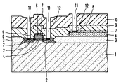
- the figure shows a section of a cross section of a semiconductor arrangement, which is processed according to the inventive method.
- Active structures 2 are formed on a silicon substrate 1 for insulation purposes are surrounded by a field oxide layer 3.
- the active structures 2 form the Source and drain regions of a MOS transistor.
- Over the gate area 4 of the MOS transistor is formed with a thin gate oxide film 5.
- On the gate oxide film 5 and a partial area of the field oxide layer 3 has a polysilicon layer 6 applied.
- One is on the active structures 2 and on the structured polysilicon layer 6 Contact layer 7 made of a conductive material to form conductive Areas applied.
- An insulator layer 9 is applied to this arrangement, which can also comprise several insulating layers.
- the insulator layer 9 has a planarizing property for the surface of the semiconductor device. Out of it it follows that the insulator layer 9 different thickness over the cross section of the Has semiconductor arrangement.
- the insulator layer 9 can consist of layers Silicon oxide and silicon nitride exist.
- An etching mask is on the insulator layer 9 10 applied, which openings 11 for creating contact holes for Contacting the
- the semiconductor device is shown in the state in which according to the Method according to the invention, contact holes 12 have been etched into the insulator layer 9 are. As a result, the conductive regions 8 that are to be contacted are exposed.
- the semiconductor arrangement shown in FIG given an etching device.
- the semiconductor arrangement is in the etching device exposed to a plasma etching process.
- the device becomes a gas mixture supplied which argon as a carrier gas, fluorinated carbon, fluorinated Contains hydrocarbon and oxygen as a reactive etching gas.
- the gas mixture will fed to the etching device in such a way that a pressure arises during the etching process, which is between 150 mT to 900 mT.
- the proportion of argon is between 25% and 75%, the proportion of fluorinated carbon between 8% and 25%, the proportion of fluorinated hydrocarbon between 15% and 45% and the proportion of oxygen between 1% and 20% of the total gas flow.
- the plasma etching process is used at a frequency of some 100 kH. Due to the relatively slow Alternating frequency of this plasma excitation creates a relatively high ion energy Etching radicals. This results in a high etching rate for the material to be etched, i.e. achieved in particular for the insulator layer 9.
- the oxygen causes the material the conductive areas 8, which is preferably made of silicon siliconized with titanium consists of monocrystalline or polycrystalline silicon can be oxidized. As a result, the removal rate increases in the conductive areas 8 of the material in the etching process. However, the oxidized surface removed at the same time in the process, so that the surface of the conductive areas 8 becomes conductive again.
- the insulator layer 9 which is used to planarize the surface of the semiconductor wafer is used, different thicknesses along the semiconductor cross section.
- the thickness of the insulator layer 9 in the arrangement shown in the areas of the active structures 2 to be contacted on the left-hand side of the Figure is considerably larger than in the conductive region 8 to be contacted Conductor over the field oxide layer 3 on the right side of the figure. It is through the inventive method prevents the area 8 to be contacted from the right side of the figure, which is introduced over the field oxide layer 3, overetched becomes, while the conductive region 8 on the left side of the figure becomes Contacting the active structures 2 still needs to be exposed.
- the etching mask 10 is removed. After that a material suitable for contacting the conductive areas 8, for example Aluminum, titanium, etc. introduced into the contact holes 12 produced.
Landscapes
- Drying Of Semiconductors (AREA)
- Internal Circuitry In Semiconductor Integrated Circuit Devices (AREA)
Applications Claiming Priority (2)
| Application Number | Priority Date | Filing Date | Title |
|---|---|---|---|
| DE19707886 | 1997-02-27 | ||
| DE19707886A DE19707886C2 (de) | 1997-02-27 | 1997-02-27 | Verfahren zum Erzeugen von Kontaktlöchern in einer Halbleiteranordnung |
Publications (2)
| Publication Number | Publication Date |
|---|---|
| EP0862206A2 true EP0862206A2 (fr) | 1998-09-02 |
| EP0862206A3 EP0862206A3 (fr) | 2000-02-23 |
Family
ID=7821668
Family Applications (1)
| Application Number | Title | Priority Date | Filing Date |
|---|---|---|---|
| EP98102592A Withdrawn EP0862206A3 (fr) | 1997-02-27 | 1998-02-14 | Gravure de trous de contact dans un dispositif semiconducteur |
Country Status (4)
| Country | Link |
|---|---|
| EP (1) | EP0862206A3 (fr) |
| JP (1) | JPH10321597A (fr) |
| DE (1) | DE19707886C2 (fr) |
| TW (1) | TW394991B (fr) |
Cited By (1)
| Publication number | Priority date | Publication date | Assignee | Title |
|---|---|---|---|---|
| WO2006019572A1 (fr) * | 2004-07-21 | 2006-02-23 | Hewlett-Packard Development Company, L.P. | Gravure par attraction électrostatique d'ions |
Families Citing this family (1)
| Publication number | Priority date | Publication date | Assignee | Title |
|---|---|---|---|---|
| DE10053780A1 (de) * | 2000-10-30 | 2002-05-16 | Infineon Technologies Ag | Verfahren zur Strukturierung einer Siliziumoxid-Schicht |
Family Cites Families (10)
| Publication number | Priority date | Publication date | Assignee | Title |
|---|---|---|---|---|
| US4376672A (en) * | 1981-10-26 | 1983-03-15 | Applied Materials, Inc. | Materials and methods for plasma etching of oxides and nitrides of silicon |
| US4465552A (en) * | 1983-08-11 | 1984-08-14 | Allied Corporation | Method of selectively etching silicon dioxide with SF6 /nitriding component gas |
| US4657628A (en) * | 1985-05-01 | 1987-04-14 | Texas Instruments Incorporated | Process for patterning local interconnects |
| JPH0680643B2 (ja) * | 1986-05-19 | 1994-10-12 | 株式会社日立製作所 | シリコン酸化膜のエツチング方法 |
| JP2798944B2 (ja) * | 1988-06-09 | 1998-09-17 | 三菱電機株式会社 | 薄膜形成方法 |
| US5549784A (en) * | 1992-09-04 | 1996-08-27 | Intel Corporation | Method for etching silicon oxide films in a reactive ion etch system to prevent gate oxide damage |
| US5468340A (en) * | 1992-10-09 | 1995-11-21 | Gupta; Subhash | Highly selective high aspect ratio oxide etch method and products made by the process |
| JPH06163470A (ja) * | 1992-11-24 | 1994-06-10 | Sumitomo Metal Ind Ltd | エッチング方法 |
| KR950033669A (ko) * | 1994-01-27 | 1995-12-26 | 제임스 조셉 드롱 | 산화물, 규화물 및 실리콘에 대하여 선택성을 갖는 질화물 식각공정 |
| TW295695B (fr) * | 1994-09-19 | 1997-01-11 | Motorola Inc |
-
1997
- 1997-02-27 DE DE19707886A patent/DE19707886C2/de not_active Expired - Fee Related
-
1998
- 1998-02-14 EP EP98102592A patent/EP0862206A3/fr not_active Withdrawn
- 1998-02-23 TW TW087102544A patent/TW394991B/zh not_active IP Right Cessation
- 1998-02-26 JP JP10045963A patent/JPH10321597A/ja not_active Withdrawn
Cited By (5)
| Publication number | Priority date | Publication date | Assignee | Title |
|---|---|---|---|---|
| WO2006019572A1 (fr) * | 2004-07-21 | 2006-02-23 | Hewlett-Packard Development Company, L.P. | Gravure par attraction électrostatique d'ions |
| US7183215B2 (en) | 2004-07-21 | 2007-02-27 | Hewlett-Packard Development Company, L.P. | Etching with electrostatically attracted ions |
| GB2431129A (en) * | 2004-07-21 | 2007-04-18 | Hewlett Packard Development Co | Etching with electrostatically attracted ions |
| GB2431129B (en) * | 2004-07-21 | 2009-08-12 | Hewlett Packard Development Co | Etching with electrostatically attracted ions |
| DE112005001713B4 (de) * | 2004-07-21 | 2012-04-12 | Samsung Electronics Co., Ltd. | Verfahren zum Ätzen und Herstellen einer Mikrospiegelvorrichtung |
Also Published As
| Publication number | Publication date |
|---|---|
| DE19707886A1 (de) | 1998-09-10 |
| TW394991B (en) | 2000-06-21 |
| JPH10321597A (ja) | 1998-12-04 |
| DE19707886C2 (de) | 2003-12-18 |
| EP0862206A3 (fr) | 2000-02-23 |
Similar Documents
| Publication | Publication Date | Title |
|---|---|---|
| DE69616981T2 (de) | Verfahren zur ätzung eines polysiliziummusters | |
| DE68924468T2 (de) | Verfahren und Struktur zur Herstellung einer Isolierung aus VLSI- und ULSI-Schaltungen. | |
| DE68928291T2 (de) | Veraschungsverfahren zum Entfernen einer organischen Schicht auf einer Halbleiteranordnung während ihrer Herstellung | |
| DE69033615T2 (de) | Ätzen von Kontaktlöchern in einer dielektrischen Doppelschicht mit einer einzigen Ätzkammer | |
| DE68928826T2 (de) | Reaktives Ionenätzen von Silicium enthaltenden Materialien mittels Bromwasserstoff | |
| DE60129566T2 (de) | Verfahren zur selektiven ätzung von oxidschichten | |
| DE68923305T2 (de) | Elektrische Leitungen für elektronische Bauelemente. | |
| DE69025300T2 (de) | Integrierte Schaltung mit einer planarisierten dielektrischen Schicht | |
| DE4310955C2 (de) | Verfahren zum Bearbeiten eines Halbleiterwafers | |
| DE68926855T2 (de) | Trockenätzverfahren | |
| EP0094528A2 (fr) | Procédé pour la fabrication de structures à double couche comportant du silicide de métal et du polysilicium sur des substrats comportant des circuits intégrés par attaque chimique par ions réactifs | |
| DE69724192T2 (de) | Verfahren zum Ätzen von Polyzidstrukturen | |
| DE2930293A1 (de) | Aetzverfahren bei der herstellung eines gegenstandes | |
| DE3627311A1 (de) | Verfahren zum aetzen von silizium | |
| DE10224935A1 (de) | Verfahren zum Ätzen von Öffnungen mit hohem Seitenverhältnis | |
| DE69626562T2 (de) | Verfahren zum isotropen Ätzen von Silizium, das hochselektiv gegenüber Wolfram ist | |
| DE4130391C2 (de) | Verfahren zum selektiven entfernen einer schicht und dessen verwendung | |
| DE10101766A1 (de) | Verfahren und Vorrichtung zum Herstellen einer dünnen Schicht auf einem Substrat | |
| DE4001372A1 (de) | Verfahren zur herstellung einer halbleiteranordnung | |
| DE2930360A1 (de) | Verfahren zum plasmaaetzen von aluminium | |
| DE4139462C2 (de) | Verfahren zur Verbindung von Schichten in einer Halbleitervorrichtung | |
| DE69819023T2 (de) | Methode, eine leitende schicht zu ätzen | |
| EP0126969B1 (fr) | Procédé pour la formation de structures comportant des siliciures métalliques, en particulier en siliciure polysilicium, pour circuits intégrés à semi-conducteurs par attaque par ions réactifs | |
| EP0013711A2 (fr) | Procédé de décapage des couches de chrome | |
| DE69416808T2 (de) | Verfahren zur Herstellung einer mehrschichtigen Halbleitervorrichtung |
Legal Events
| Date | Code | Title | Description |
|---|---|---|---|
| PUAI | Public reference made under article 153(3) epc to a published international application that has entered the european phase |
Free format text: ORIGINAL CODE: 0009012 |
|
| AK | Designated contracting states |
Kind code of ref document: A2 Designated state(s): DE FR GB IT NL |
|
| AX | Request for extension of the european patent |
Free format text: AL;LT;LV;MK;RO;SI |
|
| PUAL | Search report despatched |
Free format text: ORIGINAL CODE: 0009013 |
|
| AK | Designated contracting states |
Kind code of ref document: A3 Designated state(s): AT BE CH DE DK ES FI FR GB GR IE IT LI LU MC NL PT SE |
|
| AX | Request for extension of the european patent |
Free format text: AL;LT;LV;MK;RO;SI |
|
| RAP1 | Party data changed (applicant data changed or rights of an application transferred) |
Owner name: MICRONAS GMBH |
|
| 17P | Request for examination filed |
Effective date: 20000823 |
|
| AKX | Designation fees paid |
Free format text: DE FR GB IT NL |
|
| 17Q | First examination report despatched |
Effective date: 20051111 |
|
| STAA | Information on the status of an ep patent application or granted ep patent |
Free format text: STATUS: THE APPLICATION HAS BEEN WITHDRAWN |
|
| 18W | Application withdrawn |
Effective date: 20080209 |