EP0866580A2 - Fehlerrateschätzer für PSK Signale - Google Patents
Fehlerrateschätzer für PSK Signale Download PDFInfo
- Publication number
- EP0866580A2 EP0866580A2 EP98301288A EP98301288A EP0866580A2 EP 0866580 A2 EP0866580 A2 EP 0866580A2 EP 98301288 A EP98301288 A EP 98301288A EP 98301288 A EP98301288 A EP 98301288A EP 0866580 A2 EP0866580 A2 EP 0866580A2
- Authority
- EP
- European Patent Office
- Prior art keywords
- signal
- error
- estimator
- absolute value
- phase
- Prior art date
- Legal status (The legal status is an assumption and is not a legal conclusion. Google has not performed a legal analysis and makes no representation as to the accuracy of the status listed.)
- Granted
Links
Images


Classifications
-
- H—ELECTRICITY
- H04—ELECTRIC COMMUNICATION TECHNIQUE
- H04L—TRANSMISSION OF DIGITAL INFORMATION, e.g. TELEGRAPHIC COMMUNICATION
- H04L1/00—Arrangements for detecting or preventing errors in the information received
- H04L1/20—Arrangements for detecting or preventing errors in the information received using signal quality detector
- H04L1/206—Arrangements for detecting or preventing errors in the information received using signal quality detector for modulated signals
-
- H—ELECTRICITY
- H04—ELECTRIC COMMUNICATION TECHNIQUE
- H04B—TRANSMISSION
- H04B1/00—Details of transmission systems, not covered by a single one of groups H04B3/00 - H04B13/00; Details of transmission systems not characterised by the medium used for transmission
- H04B1/06—Receivers
- H04B1/10—Means associated with receiver for limiting or suppressing noise or interference
Definitions
- the present invention relates to an estimator of error rate which is suitably used for a radio receiving system for digital mobile communications or the like, and more particularly to the estimator of error rate which operates to estimate an error rate through the use of phase information and envelope information of a received baseband signal.
- a radio receiving system for digital mobile communications such as a portable phone is required to estimate an error rate, because the system has to perform various controls according to the error rate of the received signal.
- the system employs a technique of estimating the error rate under the certain conditions. For example, if the received signal is close to a threshold value of a middle betweem signal points, under a certain condition, the received signal may be estimated as an error with a probability of 50 percents. Hence, by counting the signal closing to the threshold value, it is possible to estimate the error rate.
- Fig. 9 shows an arrangement of a conventional estimator of error rate.
- a memory 1 operates to generate phase information 8 from a baseband signal 6 of an I channel (I signal) and a baseband signal 7 of a Q channel (Q signal).
- a delaying unit 2 operates to delay an input signal by one symbol period.
- a subtracter 3 operates to subtract the phase information of one symbol past from the phase information at the current time point.
- a coincidence detector 4 operates to generate an error pulse only if the input signal coincides with a signal for representing an error pulse generation area.
- a counter 5 operates to count the number of error pulses.
- an I signal 6 and a Q signal 7 are inputted to the addresses of the memory 1.
- the I signal 6 is a baseband signal of the I channel derived by orthogonally detecting the received signal.
- the Q signal 7 is a baseband signal of the Q channel derived by the same manner.
- the memory 1 stores the phase information arctan(Q/I) of the I signal 6 and the Q signal. Then, by reading out the phase information from the memory 1, it is possible to obtain the phase information 8 of the I signal 6 and the Q signal 7.
- phase information 8 is delayed by one symbol period through the effect of the delaying unit 2. This delay is required for demodulating an original signal from a differential phase modulated signal by the delaying detection. Then, the subtracter 3 operates to subtract the delayed phase information from the phase information 8 for deriving a delayed detection signal 10.
- the delayed detection signal 10 is inputted to the coincidence detector 4, in which if the signal 10 coincides with the signal 11 for representing the error pulse generation area, an error pulse signal 12 can be obtained. If the delayed detection signal 10 is close to a border value, the signal is estimated as an error signal with a probability of 50 percents. Hence, by setting the error pulse generation area to a value close to the border value, it is possible to obtain the information for estimating the error.
- an error pulse signal 12 is inputted into the counter 5.
- the counter 5 operates to count the number of error pulses at each burst signal and then supply a signal 13 for representing the number of error pulse counts.
- the estimator of error rate arranged as described above uniformly sets the error pulse generation area relative to the phase information and generates the error pulse if the phase information coincides with the error pulse generation area.
- the estimator is requested to count signals that are less probably estimated as error ones if the other conditions are changed.
- the variations of the count value at each burst signal take place, which result in disadvantageously lowering an accuracy of estimating an error rate.
- the conventional estimator of error rate is arranged to estimate an error rate on the basis of only the fact that the phase information is close to the border value for determining the phase and to set certain values before and after the border value as the error pulse generation area. If the envelope information is close to a reference value, an error takes place only around the border value for phase determination. The probability that the received signal is not erroneous is high at both edges of the set error pulse generation area. Hence, the estimator counts the non-erroneous signals in some states of the envelope information, so that variations of the count value may take place.
- the JP-A-59-200547 has disclosed provision of means for detecting an error of a channel by referring to a predetermined syndrome in a receive demodulating system apparatus located in a terminal apparatus and/or a relay apparatus.
- detection of an error on the syndrome needs a complicated calculation and a considerably long time and large circuit scale.
- the error rate is equal to or larger than a certain value, though an error itself can be detected, the number of errors, that is, the error rate cannot be grasped.
- the present invention is made in consideration of the foregoing shortcomings, and it is an object of the present invention to provide an estimator of error rate which is arranged to estimate an error rate with high accuracy and at fast speed though it is composed of a relatively simple circuit.
- an estimator for estimating an error rate of data included in a phase shift keying (PSK) signal comprises a phase information generator for detecting from the received PSK signal a first baseband signal in a first detection axis and a second baseband signal in a second detection axis and generating phase information of the PSK signal based on at least the first and the second baseband signals, an envelope information generator for generating envelope information of the PSK signal based on at least the first and the second baseband signals, a phase error detector for outputting a phase error signal when the phase information indicates the PSK signal is located in the predetermined phase area, an envelope error detector for outputting an envelope error signal when the envelope information indicates the PSK signal is located in the predetermined envelope area, means for outputting an error signal in presence of both the phase error signal and the envelope error signal, and a counter for counting the error signals for a predetermined time period and outputting a count value.
- PSK phase shift keying
- This arrangement makes it possible to estimate the error rate based on the phase information and the envelope information of the PSK signal, thereby improving the estimating accuracy further than the conventional estimator arranged to use only the phase information for the estimation though it needs the substantially same time for the estimation as the conventional estimator.
- the radio receiving system for digital mobile communications is arranged to orthogonally detect the received signal for deriving a baseband signal of an I channel (I signal) and a baseband signal of a Q channel (Q signal), obtain the phase information by arctan(Q/I), take a difference between the phase information and a signal delayed by one symbol, and derive the resulting delayed phase information.
- the signal points are ⁇ /4 and ⁇ 3 ⁇ /4
- the border points are determined as 0, ⁇ and ⁇ /2. If the phase information is close to 0, ⁇ and ⁇ /2, it is estimated that the signal is erroneous with a probability of 50 percents. Hence, the signal is estimated to be erroneous with a high probability. That is, around the border points, the signal is determined to be a meaningless signal as a binary signal.
- the reference value is 1, it is considered that no error takes place in the envelope information if the envelope information is closer to one. Conversely, if the envelope information is close to zero, it is considered that the signal is erroneous with a high probability. Further, if the envelope information is far larger than one, the signal is estimated to be erroneous with a high probability. Hence, when the envelope information is close to the reference value, there is a high probability that the signal is not erroneous. It means that the envelope information is not approximate to estimating an error rate.
- the envelope information is around zero or far larger than 1 and the phase information is close to 0, ⁇ or ⁇ /2, it is considered that there exists a high probability that it is an error signal. That is, the signal in this area is equivalent to the noise as a binary signal. Hence, by counting the signals for meeting these two conditions, it is possible to estimate the error rate. Further, since the area does not contain the area of a low probability that the signal is an error signal, the erroneous difference among the error pulse counts of certain intervals is made lower.
- the estimator of error rate operates to count only the signals for meeting the condition that the phase information is close to a threshold value for determining the phase, in the state that the envelope information is close to zero or larger than the reference value, for estimating the error rate based on the count value.
- the estimator enables to output a correct error rate with a small estimating error.
- the estimator of error rate is arranged to detect that both of the phase information and the envelope information contained in the baseband signal of the I channel (I signal) and the baseband signal of the Q channel (Q signal) derived from the received signal are located in the corresponding error pulse generation areas and to estimate the error rate based on the detected result.
- Fig. 1 shows the arrangement of the estimator of error rate.
- a reference number 1 denotes a memory for generating the phase information from the I signal and the Q signal.
- a reference number 2 denotes a delaying unit for delaying an input signal by one symbol period.
- a reference number 3 denotes a subtracter for subtracting the phase information of one symbol past from the phase information at the current time point.
- a reference number 4 denotes a coincidence detector for generating an error pulse if the input signal coincides with the signal for representing the error pulse generation area.
- a reference number 5 denotes a counter for counting the number of error pulses.
- a reference number 14 denotes a memory for generating the envelope information from the I signal and the Q signal.
- a reference number 20 denotes a subtracter for subtracting a reference value from the envelope information of the I and the Q signals.
- a reference number 16 denotes an absolute value detector for calculating an absolute value of the input signal.
- a reference number 17 denotes a subtracter for subtracting a threshold value from the absolute value of the difference between the envelope information and the reference value derived by the absolute detector 16.
- a reference number 18 denotes a determining unit for determining the input signal.
- a reference number 19 denotes an AND circuit for taking a logical product of the input signals
- the I signal 6 and the Q signal 7 are inputted to the addresses of the memory 1.
- the phase information 8 of the I signal 6 and the Q signal 7 can be obtained.
- the phase information 8 is delayed by one symbol period through the effect of the delaying unit 2.
- the subtracter 3 operates to subtract the delayed phase signal from the phase information 8 and then feed a delayed detection signal 10.
- the delayed detection signal 10 is inputted to the coincidence detector 4.
- the coincidence detector 4 operates to output an error pulse signal 12 of the phase information if the the signal 10 coincides with the signal 11 for representing the error pulse generation area of the phase information.
- the I signal 6 and the Q signal 7 are inputted to the addresses of the memory 14.
- the memory 14 stores the envelope information ⁇ (I 2 + Q 2 ) of the I signal 6 and the Q signal 7.
- the subtracter 15 operates to subtract a reference value 21 from the envelope information 20 and output a signal 22 for representing the difference between the reference value and the envelope information of the I signal 6 and the Q signal 7.
- the absolute value of the signal 22 is detected by the absolute value detector 16.
- the detector 16 outputs a signal 23 for representing the absolute value of the difference between the reference value and the envelope information of the I signal 6 and the Q signal 7.
- the signal 23 is sent to the subtracter 17 in which a threshold value 24 is subtracted from the signal 23.
- the subtracter 17 outputs the resulting signal 25.
- the signal 25 is inputted to the determining unit 18. If the signal 25 exceeds the threshold value 24, the determining unit 18 operates to output an error pulse signal 26 of the envelope information. If the envelope information is separated from the reference value by a certain value or more, the determining unit 18 operates to output an error pulse signal of the envelope information. That is, if the envelope information is close to zero or far larger than the reference value, the signal is estimated as an error signal.
- the error pulse signal 12 of the phase information and the error pulse signal of the envelope information are inputted to the AND circuit 19.
- the AND circuit 19 operates to take a logical product of both signals and output an error pulse signal 27 for meeting the error pulse generation areas of the phase information and the envelope information of the I signal 6 and the Q signal 7.
- the error pulse signal 27 is inputted into the counter 5 operates to count the number of error pulses at each burst signal and output the signal for representing the error pulse count.
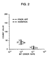
- Fig. 2 shows the simulated result of the bit error rate and the error pulse count. From the graph of Fig. 2, the following result is obtained.
- the estimator of this embodiment enables to reduce the difference between a maximum count number and a minimum count number (for representing variations of the error pulse count numbers at the burst signals) into a factor of 2/3 rather than the conventional estimator.
- the estimator of error rate operates to reduce the difference between the maximum count number and the minimum count number of the error pulse (representing variations of the error pulse count numbers at the burst signals) and thereby estimate the error rate with high accuracy.
- the estimator is just required to count only the signals in which the phase information is very close to the border value and the envelope information is far separate from the reference value and thereby to estimate the error rate more accurately.
- the error pulse generation area is made variable according to the error rate so that the variations of the count value are reduced. In the second embodiment, therefore, the error pulse generation area is switched according to the error rate.
- the estimator of the second embodiment provides means for varying the phase error pulse generation area in the phase error detector.
- the estimator operates to detect that both the phase information signal and the envelope information signal derived from the baseband signal of the I channel (I signal) and the baseband signal of the Q channel (Q signal) are located in the corresponding error pulse generation areas and thereby to estimate the error rate.
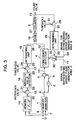
- Fig. 3 shows the estimator of error rate according to the second embodiment of the invention.
- the different respects of the second embodiment from the first embodiment are provision of a subtracter 28, a determining unit 29, and a switch 30 and that the signal for representing the error pulse generation area in the phase information is variable.
- the subtracter 28 operates to subtract a threshold value 31 from the error pulse count value 13 and output it as a difference signal 32.
- the signal is inputted to the determining unit 29 in which it is determined if the signal 32 is positive or negative. Then, the determining unit 29 operates to output a control signal 33.
- the switch 30 operates to select a signal 11 (signal A for representing the error pulse generation area) or a signal 34 (signal B for representing the error pulse generation area) according to the control signal 33 and then output a signal 35 for representing the error pulse generation area of the phase information.
- the estimator excludes the operation of counting signals that are less probably estimated as error signals and thereby operates to estimate the error rate more accurately.
- the estimator of the second embodiment operates to reduce the difference between the maximum count value and the minimum count value of the error pulse (variations of the error pulse count values at the burst signals) rather than the estimator of the first embodiment and thereby to estimate the error rate more accurately.
- the estimator of error rate provides means for varying the error pulse generation area in both of the phase error detector and the envelope error detector.
- the estimator of error rate operates to detect that both of the phase information signal and the envelope information signal derived from the baseband signal of the I channel (I signal) and the baseband signal of the Q channel (Q signal) are located in the corresponding error pulse generation areas and thereby to stimate the error rate.
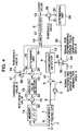
- Fig. 4 shows the estimator of error rate according to this embodiment of the invention.
- the different respects of the third embodiment from the second embodiment are provision of a switch 36 and that the signals for representing the error pulse generation areas in both of the phase information and the envelope information are variable.
- the switch 36 operates to switch the signal 24 (threshold value C) or a signal 37 (threshold value D) according to the control signal 33 and output the threshold value 38. If the count value 13 is smaller than the threshold value 31, the switch 36 operates to select a larger threshold value according to the control signal 33. If the count value 13 is larger than the threshold value 31, the switch 36 operates to select a smaller threshold value.
- the estimator enables to estimate the error rate more accurately.
- the error pulse generation area contains the area having a far larger value than the reference value of the envelope information. The influence of the area can be ignored, because few signals are allowed to be entered into the area.
- the estimator of error rate according to the third embodiment includes the variable signals for representing the error pulse generation areas of the phase information and the envelope information.
- the estimator enables to reduce the difference between the maximum count value and the minimum count value of the error pulse (variations of the error pulse counts at the burst signals) more than the estimator of the second embodiment, and estimate the error rate more accurately.
- the estimator of error rate includes a phase information generator and an envelope information generator.
- the phase information generator is composed of an absolute value circuit, a subtracter, a quadrant determining unit and a converter.
- the envelope information generator is composed of a comparator, a shift circuit and an adder.
- the estimator operates to detect that the phase information signal and the envelope information signal derived from the received baseband signal of the I channel (I signal) and the received baseband signal of the Q channel (Q signal) are located in the corresponding error pulse generation areas and estimate the error rate based on the detected result.
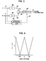
- Fig. 5 shows an example of the phase information generator included in the fourth embodiment.
- Fig. 7 shows an example of the envelope information generator included in the fourth embodiment.
- the different respect of the fourth embodiment from the first to the third embodiments is that neither of the phase information generator and the envelope information generator contain any memory.
- the phase ⁇ may be generated within an error of 1.8 degree by doing the approximation shown in the expression (1).
- the phases ⁇ of the I and the Q signals are ⁇ /4 and ⁇ 3 ⁇ /4 if the I and the Q signals both have the reference values. If one of the I and the Q signals is zero and the other has the reference value, the phases q are ⁇ and ⁇ /2.
- the phase ⁇ is close to ⁇ /4,
- ⁇ -4 ⁇ / ⁇ + 1 is established at the second to the fourth quadrants.
- the similar approximations may be made. Under the condition that the I and the Q signals are close to ⁇ 1, the expression (1) makes a good approximation. If the condition is not met, the error is increased. If it is necessary to reduce the error, the I and the Q signals are just required to be regulated.
- the I signal 6 and the Q signal 7 are inputted into an absolute value detector 39 and an absolute value detector 40, in which the absolute values of the I and the Q signals 6 and 7 are calculated.
- the detectors 39 and 40 operate to output the absolute value signals 44 and 45.
- the signals 44 and 45 are subtracted by a subtracter 41.
- the subtracter 41 operates to output a difference signal 46.
- the I signal 6 and the Q signal 7 are inputted into a quadrant determining unit 42.
- the determining unit 42 outputs a signal for representing the quadrant.
- the difference signal 46 is converted according to each quadrant by a converter 43.
- the converter 43 operates to output the phase information 8.
- Fig. 8 shows the relation between the phase ⁇ and the presumed radius Z about the I and the Q signals.
- Z may be generated within the error of 7% by making the approximation shown in the expression (2). This small degree of error gives no obstacle to presuming the error rate.
- the I signal 6 is compared in magnitude with the Q signal 7 by a magnitude comparator 48.
- the comparator 48 feeds a signal 53 (
- the signal 54 is shifted by two bits by a 2-bits shifter 49 and by three bits by a 3-bits shifter 50 in parallel.
- the shifter 49 outputs a signal (signal 54 • 0.25) and the shifter 50 outputs a signal (signal 54 • 0.125).
- the signals 55 and 56 are added by an adder 51.
- the adder 51 outputs a signal 57 (signal 54 • 0.375).
- the signals 53 and 57 are added by an adder 52. Then, the adder 52 outputs the envelope information 20.
- the estimator of the fourth embodiment does not include any memory for composing the phase information generator and the envelope information generator.
- the estimator of the fourth embodiment enables to estimate an error more faster than the estimators of the first to the third embodiments and speed up the signal transmission speed because it is not limited by the time consumed by the error estimation.
- the estimator of error rate according to the present invention is arranged to use both of the phase information and the envelope information derived from plural baseband signals (Q signals) for reducing a difference between the maximum count value and the minimum count value of the error pulse (the variations of the error pulse count values at the burst signals, thereby being able to more accurately estimate the error rate.
- the estimator enables to change the error pulse generation area according to the error rate, so that it may estimate the error rate with less variation.
- the estimator of error rate enables to obtain the phase information and the envelope information with a simple circuit and at fast speed. Hence, the estimator speeds up the error estimation and the signal transmission speed.
Landscapes
- Engineering & Computer Science (AREA)
- Computer Networks & Wireless Communication (AREA)
- Signal Processing (AREA)
- Quality & Reliability (AREA)
- Digital Transmission Methods That Use Modulated Carrier Waves (AREA)
- Detection And Prevention Of Errors In Transmission (AREA)
- Noise Elimination (AREA)
Applications Claiming Priority (3)
| Application Number | Priority Date | Filing Date | Title |
|---|---|---|---|
| JP8342397 | 1997-03-18 | ||
| JP83423/97 | 1997-03-18 | ||
| JP08342397A JP3568353B2 (ja) | 1997-03-18 | 1997-03-18 | 誤り率推定装置 |
Publications (3)
| Publication Number | Publication Date |
|---|---|
| EP0866580A2 true EP0866580A2 (de) | 1998-09-23 |
| EP0866580A3 EP0866580A3 (de) | 2001-05-02 |
| EP0866580B1 EP0866580B1 (de) | 2007-01-03 |
Family
ID=13802037
Family Applications (1)
| Application Number | Title | Priority Date | Filing Date |
|---|---|---|---|
| EP98301288A Expired - Lifetime EP0866580B1 (de) | 1997-03-18 | 1998-02-23 | Fehlerrateschätzer für PSK Signale |
Country Status (6)
| Country | Link |
|---|---|
| US (1) | US6111921A (de) |
| EP (1) | EP0866580B1 (de) |
| JP (1) | JP3568353B2 (de) |
| KR (1) | KR100269652B1 (de) |
| CN (1) | CN1106096C (de) |
| DE (1) | DE69836775T2 (de) |
Cited By (10)
| Publication number | Priority date | Publication date | Assignee | Title |
|---|---|---|---|---|
| WO2002049263A3 (en) * | 2000-12-15 | 2003-04-10 | Valence Semiconductor Inc | Blind channel estimation and data detection for psk ofdm-based receivers |
| WO2009149420A1 (en) * | 2008-06-06 | 2009-12-10 | Maxim Integrated Products, Inc. | Blind channel quality estimator |
| US8139614B2 (en) | 2008-06-06 | 2012-03-20 | Maxim Integrated Products, Inc. | Robust narrowband symbol and frame synchronizer for power-line communication |
| US8149967B2 (en) | 2008-06-06 | 2012-04-03 | Maxim Integrated Products, Inc. | Combined dual feed-forward and feedback analog and digital automatic gain control for broadband communication |
| US8165172B2 (en) | 2008-06-06 | 2012-04-24 | Maxim Integrated Products, Inc. | Robust wideband symbol and frame synchronizer for power-line communication |
| US8276025B2 (en) | 2008-06-06 | 2012-09-25 | Maxim Integrated Products, Inc. | Block interleaving scheme with configurable size to achieve time and frequency diversity |
| US8315341B2 (en) | 2008-06-06 | 2012-11-20 | Maxim Integrated Products, Inc. | Soft repetition code combiner using channel state information |
| US8315152B2 (en) | 2008-06-06 | 2012-11-20 | Maxim Integrated Products, Inc. | System and method for applying multi-tone OFDM based communications within a prescribed frequency range |
| US8320233B2 (en) | 2009-06-12 | 2012-11-27 | Maxim Integrated Products, Inc. | Transmitter and method for applying multi-tone OFDM based communications within a lower frequency range |
| US8472576B2 (en) | 2008-06-06 | 2013-06-25 | Maxim Integrated Products, Inc. | Jammer canceller for power-line communication |
Families Citing this family (5)
| Publication number | Priority date | Publication date | Assignee | Title |
|---|---|---|---|---|
| US6081822A (en) * | 1998-03-11 | 2000-06-27 | Agilent Technologies, Inc. | Approximating signal power and noise power in a system |
| KR100366293B1 (ko) * | 2000-01-28 | 2002-12-31 | 한국전자통신연구원 | 배열 송수신부의 오차 보정장치 및 방법 |
| US7076001B2 (en) * | 2001-10-16 | 2006-07-11 | Harris Corporation | System and method for an in-service decision-directed signal to noise ratio estimator |
| JP3935460B2 (ja) * | 2003-09-30 | 2007-06-20 | 松下電器産業株式会社 | 振幅情報抽出装置および振幅情報抽出方法 |
| JP4973939B2 (ja) * | 2007-10-10 | 2012-07-11 | ソニー株式会社 | 受信装置、受信方法、情報処理装置、情報処理方法、及びプログラム |
Family Cites Families (6)
| Publication number | Priority date | Publication date | Assignee | Title |
|---|---|---|---|---|
| JPS59200547A (ja) * | 1983-04-26 | 1984-11-13 | Nec Corp | 回線品質監視方式 |
| WO1991009482A1 (en) * | 1989-12-07 | 1991-06-27 | The Commonwealth Of Australia | Error rate monitor |
| US5249204A (en) * | 1991-08-12 | 1993-09-28 | Motorola, Inc. | Circuit and method for phase error correction in a digital receiver |
| JP2848420B2 (ja) * | 1991-10-16 | 1999-01-20 | 富士通株式会社 | バースト信号検出装置および方法 |
| US5631554A (en) * | 1993-03-26 | 1997-05-20 | Schlumberger Industries, Inc. | Electronic metering device including automatic service sensing |
| JPH08307283A (ja) * | 1995-03-09 | 1996-11-22 | Oki Electric Ind Co Ltd | 最尤系列推定器及び最尤系列推定方法 |
-
1997
- 1997-03-18 JP JP08342397A patent/JP3568353B2/ja not_active Expired - Fee Related
-
1998
- 1998-02-23 DE DE69836775T patent/DE69836775T2/de not_active Expired - Fee Related
- 1998-02-23 EP EP98301288A patent/EP0866580B1/de not_active Expired - Lifetime
- 1998-02-24 US US09/028,853 patent/US6111921A/en not_active Expired - Fee Related
- 1998-03-06 KR KR1019980007531A patent/KR100269652B1/ko not_active Expired - Fee Related
- 1998-03-17 CN CN98105720A patent/CN1106096C/zh not_active Expired - Fee Related
Cited By (17)
| Publication number | Priority date | Publication date | Assignee | Title |
|---|---|---|---|---|
| WO2002049263A3 (en) * | 2000-12-15 | 2003-04-10 | Valence Semiconductor Inc | Blind channel estimation and data detection for psk ofdm-based receivers |
| US6983029B2 (en) | 2000-12-15 | 2006-01-03 | Maxim Integrated Products, Inc. | Blind channel estimation and data detection for PSK OFDM-based receivers |
| US8315341B2 (en) | 2008-06-06 | 2012-11-20 | Maxim Integrated Products, Inc. | Soft repetition code combiner using channel state information |
| US8315152B2 (en) | 2008-06-06 | 2012-11-20 | Maxim Integrated Products, Inc. | System and method for applying multi-tone OFDM based communications within a prescribed frequency range |
| US8149967B2 (en) | 2008-06-06 | 2012-04-03 | Maxim Integrated Products, Inc. | Combined dual feed-forward and feedback analog and digital automatic gain control for broadband communication |
| US8165172B2 (en) | 2008-06-06 | 2012-04-24 | Maxim Integrated Products, Inc. | Robust wideband symbol and frame synchronizer for power-line communication |
| US8276025B2 (en) | 2008-06-06 | 2012-09-25 | Maxim Integrated Products, Inc. | Block interleaving scheme with configurable size to achieve time and frequency diversity |
| US8284825B2 (en) | 2008-06-06 | 2012-10-09 | Maxim Integrated Products, Inc. | Blind channel quality estimator |
| WO2009149420A1 (en) * | 2008-06-06 | 2009-12-10 | Maxim Integrated Products, Inc. | Blind channel quality estimator |
| US8139614B2 (en) | 2008-06-06 | 2012-03-20 | Maxim Integrated Products, Inc. | Robust narrowband symbol and frame synchronizer for power-line communication |
| US9054786B2 (en) | 2008-06-06 | 2015-06-09 | Maxim Integrated Products, Inc. | System and method for applying multi-tone OFDM based communications within a prescribed frequency range |
| US8472576B2 (en) | 2008-06-06 | 2013-06-25 | Maxim Integrated Products, Inc. | Jammer canceller for power-line communication |
| US8582668B2 (en) | 2008-06-06 | 2013-11-12 | Maxim Integrated Products, Inc. | Soft repetition code combiner using channel state information |
| US8780691B2 (en) | 2008-06-06 | 2014-07-15 | Maxim Integrated Products, Inc. | System and method for applying multi-tone OFDM based communications within a prescribed frequency range |
| US8848836B2 (en) | 2008-06-06 | 2014-09-30 | Maxim Integrated Products, Inc. | Jammer canceller for power-line communication |
| US8879379B1 (en) | 2009-06-12 | 2014-11-04 | Maxim Integrated Products, Inc. | Transmitter and method for applying multi-tone OFDM based communications within a lower frequency range |
| US8320233B2 (en) | 2009-06-12 | 2012-11-27 | Maxim Integrated Products, Inc. | Transmitter and method for applying multi-tone OFDM based communications within a lower frequency range |
Also Published As
| Publication number | Publication date |
|---|---|
| JPH10262023A (ja) | 1998-09-29 |
| EP0866580A3 (de) | 2001-05-02 |
| US6111921A (en) | 2000-08-29 |
| EP0866580B1 (de) | 2007-01-03 |
| DE69836775T2 (de) | 2007-10-31 |
| KR19980079997A (ko) | 1998-11-25 |
| JP3568353B2 (ja) | 2004-09-22 |
| DE69836775D1 (de) | 2007-02-15 |
| KR100269652B1 (ko) | 2000-10-16 |
| CN1106096C (zh) | 2003-04-16 |
| CN1196621A (zh) | 1998-10-21 |
Similar Documents
| Publication | Publication Date | Title |
|---|---|---|
| US6111921A (en) | Estimator of error rate | |
| US6788749B2 (en) | Erasure based instantaneous loop control in a data receiver | |
| US5550506A (en) | DQPSK demodulator capable of improving a symbol error rate without decreasing a transmission rate | |
| US5497400A (en) | Decision feedback demodulator with phase and frequency estimation | |
| US5694440A (en) | Data synchronizer lock detector and method of operation thereof | |
| US5511097A (en) | Delay detection circuit | |
| US5799242A (en) | Communication control unit for mobile communication systems and the like, including a channel quality detection unit, a quality decision unit and a control unit | |
| EP0153194B1 (de) | Gerät zur Aufhebung periodischer Trägerphasenschwankungen | |
| JP4166342B2 (ja) | デジタル送信信号の受信機のためのサンプリング制御ループ | |
| JP3636397B2 (ja) | ジッタ抑圧回路 | |
| US5504453A (en) | Method and device for estimating phase error | |
| KR19980071589A (ko) | 에러보정기능을 지닌 차동검파기 | |
| US5490148A (en) | Bit error rate estimator | |
| JP2000049881A (ja) | 通信システム | |
| EP1851895A1 (de) | Verfahren und vorrichtung zur signalqualitätsschätzung | |
| JP3006382B2 (ja) | 周波数オフセット補正装置 | |
| EP2930897B1 (de) | Differentielle demodulationsvorrichtung und differentielles demodulationsverfahren | |
| JPH09246917A (ja) | 周波数誤差推定装置 | |
| JP3547991B2 (ja) | 回線品質推定装置及びその方法 | |
| KR100299956B1 (ko) | Qam복조기의위상에러각에대한사인/코사인값의직접추출회로및그방법 | |
| US5953385A (en) | Method and device for detecting the error on the frequency of a carrier | |
| JP2990044B2 (ja) | 遅延検波器 | |
| KR100480691B1 (ko) | 방송수신시스템의복조기와디코더인터페이스장치 | |
| CN107395318B (zh) | 讯频图选择装置与方法 | |
| JPH08102727A (ja) | 誤り率推定方式 |
Legal Events
| Date | Code | Title | Description |
|---|---|---|---|
| PUAI | Public reference made under article 153(3) epc to a published international application that has entered the european phase |
Free format text: ORIGINAL CODE: 0009012 |
|
| 17P | Request for examination filed |
Effective date: 19980228 |
|
| AK | Designated contracting states |
Kind code of ref document: A2 Designated state(s): DE FR GB SE |
|
| AX | Request for extension of the european patent |
Free format text: AL;LT;LV;MK;RO;SI |
|
| RIN1 | Information on inventor provided before grant (corrected) |
Inventor name: UESUGI, MITSURU Inventor name: HIRAMATSU, KATUSHIKO Inventor name: SUDO, HIROAKI |
|
| PUAL | Search report despatched |
Free format text: ORIGINAL CODE: 0009013 |
|
| AK | Designated contracting states |
Kind code of ref document: A3 Designated state(s): AT BE CH DE DK ES FI FR GB GR IE IT LI LU MC NL PT SE |
|
| AX | Request for extension of the european patent |
Free format text: AL;LT;LV;MK;RO;SI |
|
| RIC1 | Information provided on ipc code assigned before grant |
Free format text: 7H 04L 1/20 A, 7H 04L 1/24 B |
|
| AKX | Designation fees paid |
Free format text: DE FR GB SE |
|
| GRAP | Despatch of communication of intention to grant a patent |
Free format text: ORIGINAL CODE: EPIDOSNIGR1 |
|
| GRAS | Grant fee paid |
Free format text: ORIGINAL CODE: EPIDOSNIGR3 |
|
| RIN1 | Information on inventor provided before grant (corrected) |
Inventor name: UESUGI, MITSURU Inventor name: HIRAMATSU, KATSUHIKO Inventor name: SUDO, HIROAKI |
|
| GRAA | (expected) grant |
Free format text: ORIGINAL CODE: 0009210 |
|
| AK | Designated contracting states |
Kind code of ref document: B1 Designated state(s): DE FR GB SE |
|
| REG | Reference to a national code |
Ref country code: GB Ref legal event code: FG4D |
|
| REF | Corresponds to: |
Ref document number: 69836775 Country of ref document: DE Date of ref document: 20070215 Kind code of ref document: P |
|
| REG | Reference to a national code |
Ref country code: SE Ref legal event code: TRGR |
|
| ET | Fr: translation filed | ||
| PLBE | No opposition filed within time limit |
Free format text: ORIGINAL CODE: 0009261 |
|
| STAA | Information on the status of an ep patent application or granted ep patent |
Free format text: STATUS: NO OPPOSITION FILED WITHIN TIME LIMIT |
|
| 26N | No opposition filed |
Effective date: 20071005 |
|
| PGFP | Annual fee paid to national office [announced via postgrant information from national office to epo] |
Ref country code: SE Payment date: 20080219 Year of fee payment: 11 Ref country code: GB Payment date: 20080220 Year of fee payment: 11 Ref country code: DE Payment date: 20080221 Year of fee payment: 11 |
|
| PGFP | Annual fee paid to national office [announced via postgrant information from national office to epo] |
Ref country code: FR Payment date: 20080208 Year of fee payment: 11 |
|
| EUG | Se: european patent has lapsed | ||
| GBPC | Gb: european patent ceased through non-payment of renewal fee |
Effective date: 20090223 |
|
| REG | Reference to a national code |
Ref country code: FR Ref legal event code: ST Effective date: 20091030 |
|
| PG25 | Lapsed in a contracting state [announced via postgrant information from national office to epo] |
Ref country code: DE Free format text: LAPSE BECAUSE OF NON-PAYMENT OF DUE FEES Effective date: 20090901 |
|
| PG25 | Lapsed in a contracting state [announced via postgrant information from national office to epo] |
Ref country code: GB Free format text: LAPSE BECAUSE OF NON-PAYMENT OF DUE FEES Effective date: 20090223 Ref country code: FR Free format text: LAPSE BECAUSE OF NON-PAYMENT OF DUE FEES Effective date: 20090302 |
|
| PG25 | Lapsed in a contracting state [announced via postgrant information from national office to epo] |
Ref country code: SE Free format text: LAPSE BECAUSE OF NON-PAYMENT OF DUE FEES Effective date: 20090224 |