EP2930897B1 - Differentielle demodulationsvorrichtung und differentielles demodulationsverfahren - Google Patents
Differentielle demodulationsvorrichtung und differentielles demodulationsverfahren Download PDFInfo
- Publication number
- EP2930897B1 EP2930897B1 EP15162376.6A EP15162376A EP2930897B1 EP 2930897 B1 EP2930897 B1 EP 2930897B1 EP 15162376 A EP15162376 A EP 15162376A EP 2930897 B1 EP2930897 B1 EP 2930897B1
- Authority
- EP
- European Patent Office
- Prior art keywords
- signal
- difference
- unit
- phase
- discrimination
- Prior art date
- Legal status (The legal status is an assumption and is not a legal conclusion. Google has not performed a legal analysis and makes no representation as to the accuracy of the status listed.)
- Active
Links
Images


Classifications
-
- H—ELECTRICITY
- H04—ELECTRIC COMMUNICATION TECHNIQUE
- H04L—TRANSMISSION OF DIGITAL INFORMATION, e.g. TELEGRAPHIC COMMUNICATION
- H04L27/00—Modulated-carrier systems
- H04L27/18—Phase-modulated carrier systems, i.e. using phase-shift keying
- H04L27/22—Demodulator circuits; Receiver circuits
-
- H—ELECTRICITY
- H04—ELECTRIC COMMUNICATION TECHNIQUE
- H04L—TRANSMISSION OF DIGITAL INFORMATION, e.g. TELEGRAPHIC COMMUNICATION
- H04L27/00—Modulated-carrier systems
- H04L27/18—Phase-modulated carrier systems, i.e. using phase-shift keying
- H04L27/22—Demodulator circuits; Receiver circuits
- H04L27/233—Demodulator circuits; Receiver circuits using non-coherent demodulation
- H04L27/2331—Demodulator circuits; Receiver circuits using non-coherent demodulation wherein the received signal is demodulated using one or more delayed versions of itself
Definitions
- This invention relates to a differential demodulator and a method for demodulating a modulated signal that has been modulated by use of a differential phase shift modulation scheme.
- DQPSK differential quadrature phase shift keying
- a demodulated signal is generated from the signal received at a certain time and the signal received just before;
- a consequent advantage of the DQPSK format is that accurate demodulation is possible even in multipath fading environments in which all received signals undergo a fixed amount of phase rotation.
- Another advantage of the DQPSK format is that accurate demodulation, substantially independent of phase rotation, is possible even in mobile reception environments in which the amount of phase rotation varies over time, provided the rate of change in the amount of phase rotation is sufficiently small in comparison with the signal transmission rate.
- Yet another advantage of the DQPSK format is that the receiver can be simplified, because the DQPSK signal does not have to reproduce an absolute phase reference in the receiver.
- Differential demodulation methods are generally used to demodulate a DQPSK signal.
- a method of differential demodulation that uses this type of calculation is disclosed in, for example, Japanese patent application publication No. H9-233138 (paragraph 0049, Fig. 2 ).
- Japanese patent application publication No. 2004-364131 paragraph 0008, Fig. 2
- paragraph 0008, Fig. 2 describes a method in which the phase plane is divided into regions, a phase reference is provided in each region, and the phase difference from the phase reference is calculated, thereby reducing the number of numerical tables or multipliers.
- EP 2 709 329 ( Fig. 1 ) also discloses a method for differential modulation.
- This problem is addressed in the present invention, the object of which is to provide a differential demodulator and a differential demodulation method that can reduce the amounts of circuitry and computation required for differential demodulation processing.
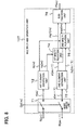
- FIG. 1 is a block diagram schematically showing the configuration of a differential demodulator 100 according to a first embodiment of the invention.
- the differential demodulator 100 is a device capable of carrying out the differential demodulation method according to the first embodiment.
- the differential demodulator 100 generates a discrimination signal (D(m), described later in FIG. 3 ) corresponding to a phase plane region in which the received signal resides, and by switching the demodulation method according to the amount of temporal variation in this discrimination signal, picks out in advance a minimal computational procedure necessary for differential demodulation.
- D(m) discrimination signal
- the calculations necessary for differential demodulation can also be simplified by restricting the content of the multiply-add computations, and the amounts of circuitry and computation necessary for the differential demodulation process can be reduced.
- the differential demodulator 100 and differential demodulation method according to the first embodiment can be applied in a receiver that receives a modulated signal that has been modulated by use of a differential phase shift keying method.
- the differential demodulator 100 in FIG. 1 receives a received signal R(m), which is a differential modulated signal, more specifically a modulated signal that has been modulated by use of the DQPSK (Differential Quadrature Phase Shift Keying) format, and outputs a differential demodulation result as a demodulated signal Z ( m ).
- the received signal R(m) and demodulated signal Z ( m ) are both complex valued signals having amplitude and phase components, and m is an integer.
- the differential demodulator 100 has a region discrimination unit 101, a discrimination signal delay unit 102, a comparison unit 103, a switching unit 104, a first decision unit 105, a received signal delay unit 106, a multiply-add operation unit 107, a second decision unit 108, and a selection unit 109.
- the received signal R ( m ) input to the differential demodulator 100 is first input to the region discrimination unit 101.
- the region discrimination unit 101 selects a residence region (one of the vertically hatched regions in FIG. 7(a) , 9(a) , 11(a) , or 13(a) ), which is a phase region in which the received signal R ( m ) resides in the phase plane (the IQ plane, as a complex number plane) from a plurality of phase regions into which the phase plane is divided according to the modulation multiplicity N of the modulated signal, and outputs a value corresponding to the residence region as the discrimination signal D ( m ).
- the plurality of phase regions are regions into which the phase plane is divided at equal phase intervals, and as the discrimination signal, values that increase counterclockwise from phase zero as a reference base are preferably assigned to each of the plurality of phase regions.
- the number of regions in the plurality of phase regions is preferably twice the modulation multiplicity N.
- the discrimination signal delay unit 102 outputs, as a delayed discrimination signal D(m - 1), a signal obtained by temporally delaying the discrimination signal D ( m ) generated by the region discrimination unit 101.
- the comparison unit 103 outputs a value corresponding to the difference between the discrimination signal D(m) and the delayed discrimination signal D(m - 1) as a difference signal Q ( m ).
- the switching unit 104 When the value of the difference signal Q ( m ) is included in a first set G1, the switching unit 104 outputs the difference signal as a first difference signal Q 1 ( m ) and outputs a selection signal C ( m ) associated with the first difference signal Q 1 ( m ) ; when the value of the difference signal Q ( m ) is included in a second set G2, the switching unit 104 outputs the difference signal as a second difference signal Q 2 ( m ) and outputs a selection signal C ( m ) associated with the second difference signal Q 2 ( m ) .
- the first set G1 is a set of difference signals such that the total size of the phase ranges in the phase plane that correspond to the difference signals Q(m) is equal to or less than the phase difference between adjacent ideal signal points in the phase plane out of a plurality of ideal signal points of the modulated signal.
- the second set G2 is a set of difference signals not included in the first set G1. The first set G1 and second set G2 will be described later.
- the first decision unit 105 generates a first decision signal X 1 ( m ) corresponding to the size of the first difference signal Q 1 ( m ).
- the received signal delay unit 106 outputs a signal obtained by temporally delaying the received signal R ( m ) as a delayed received signal R(m - 1).
- the received signal R(m) and the delayed received signal R(m - 1) are both complex valued signals.
- the multiply-add operation unit 107 refers to the received signal R(m) and the delayed received signal R(m - 1), carries out a multiply-add operation, and outputs the result of the multiply-add operation as a multiply-add output signal P(m).
- the multiply-add operation unit 107 performs multiplication operations on the imaginary part of the received signal R(m) and the real part of the delayed received signal R(m - 1), and on the real part of the received signal R(m) and the imaginary part of the delayed received signal R(m - 1), and performs a subtraction operation on a first multiplication result value obtained by multiplication of the imaginary part of the received signal R(m) and the real part of the delayed received signal R(m - 1) and a second multiplication result value obtained by multiplication of the real part of the received signal R(m) and the imaginary part of the delayed received signal R(m - 1) .
- the multiply-add operation unit 107 thereby generates the multiply-add output signal P(m) by performing only a multiplication operation on the imaginary part of the received signal R ( m ) and the real part of the delayed received signal R(m - 1), a multiplication operation on the real part of the received signal R ( m ) and the imaginary part of the delayed received signal R ( m - 1), and a subtraction operation on two real numbers.
- the second decision unit 108 generates a second decision signal X 2 ( m ) corresponding to the sizes of the second difference signal Q 2 ( m ) supplied from the switching unit 104 and the multiply-add output signal P ( m ) supplied from the multiply-add operation unit 107.
- the selection unit 109 selects one of the first decision signal and the second decision signal and outputs the selected signal as the demodulated signal Z(m).
- FIG. 2 illustrates the operation of the region discrimination unit 101 in the differential demodulator 100 according to the first embodiment.
- FIG. 2 shows an example of the relation between the plurality of phase regions used in the region discrimination unit 101 and the discrimination signals D(m) assigned to each of the phase regions.
- the phase plane IQ plane
- n is an integer such that 1 ⁇ n ⁇ 2N .
- Boundary line L(0) and boundary line L(2N) are preferably the same boundary line.
- 2N is an integer representing twice the modulation multiplicity.
- FIG. 3 also illustrates the operation of the region discrimination unit 101 in the differential demodulator 100 according to the first embodiment.
- FIG. 3 shows an example of the relation between the phase regions used in the region discrimination unit 101 and the discrimination signals assigned to them when the received signal R(m) is a DQPSK signal.
- the received signal R(m) is a DQPSK signal.
- the discrimination signal D ( m ) can be determined, for example, by referring to the signs of the received signal R(m) and the difference between the real part and the imaginary part.
- the received signal R ( m ) input to the differential demodulator 100 is input to the received signal delay unit 106 and multiply-add operation unit 107 as well as to the region discrimination unit 101. Specific examples of the operation of the received signal delay unit 106 and multiply-add operation unit 107 will be given later.
- the discrimination signal D ( m ) determined as described above is input to the discrimination signal delay unit 102.
- the input discrimination signal D(m) is held in D-flip-flops, a memory, or the like in the discrimination signal delay unit 102, and the delayed discrimination signal D ( m - 1) that was held previously is output simultaneously.
- the interval of time during which the input discrimination signal D(m) is held is preferably equal in value to the reception cycle of the received signal R ( m ) .
- the discrimination signal D ( m ) output from the region discrimination unit 101 is input to the comparison unit 103.
- the comparison unit 103 outputs the difference between the discrimination signal D(m) and the delayed discrimination signal D ( m - 1) as a difference signal Q ( m ).
- FIG. 4 is a block diagram schematically showing an example of the configuration of the comparison unit 103 in the differential demodulator 100 according to the first embodiment.
- the comparison unit 103 has a first difference operation unit 31.
- the first difference operation unit 31 calculates the difference between the discrimination signal D(m) and the delayed discrimination signal D ( m - 1), and outputs the result of this calculation as the difference signal Q ( m ).
- the first difference operation unit 31 preferably has a function such that, when the result of the difference operation on the discrimination signal D(m) and the delayed discrimination signal D ( m - 1) is negative, a modified value (a modified difference value) obtained by adding a value equal to twice the modulation multiplicity N to the result of the difference operation is output as the difference signal Q ( m ).
- the first difference operation unit 31 Since the first difference operation unit 31 has the configuration shown in FIG. 4 , it can determine the amount of phase rotation in the counterclockwise direction from the phase region in which the delayed received signal received signal R(m - 1) resides to the phase region in which the received signal R ( m ) resides.
- FIG. 5 is a block diagram schematically showing another example of the configuration of the comparison unit in the differential demodulator 100 according to the first embodiment.
- the comparison unit in FIG. 1 is indicated by reference characters 103
- reference characters 103a are assigned to the comparison unit in FIG. 5 , which has a different exemplary configuration.
- Comparison unit 103a may be configured with a first difference operation unit 31, a second difference operation unit 32, a multiplicity storage unit 33, and a minimum value selection unit 34, as shown in FIG. 5 .
- the first difference operation unit 31 calculates the difference between the discrimination signal D ( m ) and the delayed discrimination signal D(m - 1), and outputs the result of this calculation as a first candidate difference signal Q A ( m ).
- the first difference operation unit 31 preferably has a function such that, when the result of the difference operation on the discrimination signal D ( m ) and delayed discrimination signal D(m - 1) is negative, a modified value obtained by adding a value equal to twice the modulation multiplicity N to the result of the difference operation is output as the first candidate difference signal Q A ( m ).
- the second difference operation unit 32 in the comparison unit 103a preferably has a function such that the difference between the discrimination signal D ( m ) and the delayed discrimination signal D(m - 1) is simultaneously subtracted from the value equal to twice the modulation multiplicity N and the result is output as a second candidate difference signal Q B ( m ) .
- the second difference operation unit 32 preferably has a function such that, when the result of the difference operation on the discrimination signal D(m) and delayed discrimination signal D ( m - 1) is negative, a modified value obtained by adding the value equal to twice the modulation multiplicity N to the result of the difference operation is subtracted from the value equal to twice the modulation multiplicity N and the resulting value is output as the second candidate difference signal Q B ( m ).
- the minimum value selection unit 34 in the comparison unit 103a has a function of selecting the smaller value from among the first candidate difference signal Q A (m) and the second candidate difference signal Q B ( m ) ; the selected value can be output as the difference signal Q(m).
- the value of the difference signal Q ( m ) is therefore 2, this being the smaller of Q A ( m ) and Q B ( m ) .
- use of the configuration of the comparison unit 103a shown in FIG. 5 enables the differential demodulator 100 according to the first embodiment to determine the amount of phase rotation from the phase region in which the delayed received signal received signal R(m - 1) resides to the phase region in which the received signal R ( m ) resides.
- the difference signal Q ( m ) determined as described above is input to the switching unit 104.
- the switching unit 104 When the value of the input difference signal Q(m) is included in the first set G1, the switching unit 104 outputs the difference signal Q ( m ) as the first difference signal Q 1 ( m ), and outputs a selection signal C(m) associated with the first difference signal Q 1 ( m ).
- the switching unit 104 When the value of the input difference signal Q( m ) is included in the second set G2, the switching unit 104 outputs the difference signal Q ( m ) as the second difference signal Q 2 ( m ) , and outputs a selection signal C ( m ) associated with the second difference signal Q 2 ( m ).
- the switching unit 104 may be configured in such a way that when the size Wa of the phase range W of the candidate phase differences between the discrimination signal D(m) and the delayed discrimination signal D(m - 1) determined according to the difference signal Q ( m ) is within a prescribed reference phase difference A, the difference signal Q(m) is regarded as being included in the first set G1 and the difference signal Q ( m ) is output as the first difference signal Q 1 ( m ), and when the size Wa of the phase range W of the candidate phase differences between the discrimination signal D ( m ) and the delayed discrimination signal D(m - 1) determined according to the difference signal Q ( m ) exceeds the prescribed reference phase difference A, the difference signal Q ( m ) is regarded as being included in the second set G2 and the difference signal Q ( m ) is output as the second difference signal Q 2 ( m ) .
- the reference phase difference A should be the phase difference between adjacent ideal signal points in the phase plane, in the constellation
- FIG. 6 illustrates the operation of the switching unit 104 in the differential demodulator 100 according to the first embodiment.
- the received signal R(m) is a DQPSK signal and FIG. 5 is applied as the configuration of the comparison unit 103.
- the switching unit 104 When the value of the difference signal Q ( m ) is included in the first set G1, the switching unit 104 outputs the difference signal as the first difference signal Q 1 ( m ) and outputs a selection signal C ( m ) corresponding to the first difference signal Q 1 ( m ) ; when the value of the difference signal Q ( m ) is included in the second set G2, the switching unit 104 outputs the difference signal as the second difference signal Q 2 ( m ) and outputs a selection signal C ( m ) corresponding to the second difference signal Q 2 ( m ).
- the first set G1 is a set of difference signals such that the total size of the phase regions in the phase plane corresponding to the difference signals Q(m) is equal to or less than the phase difference between ideal signal points, in the constellation of ideal signal points of the modulated signal, that are adjacent in the phase plane.
- the second set G2 is the set of difference signals not included in the first set G1.
- the difference signal Q ( m ) in FIG. 6 is 0
- the sum of the sizes Wa of the phase ranges W in the phase plane that correspond to the difference signal Q ( m ) is ⁇ /2
- the constellation of ideal signal points of the modulated signal the phase difference between adjacent ideal signal points is ⁇ /2
- the sum of the sizes of the phase ranges in the phase plane corresponding to the difference signal Q( m ) is equal to or less than the phase difference between adjacent ideal signal points in the phase plane (the prescribed reference phase difference A).
- the difference signal Q ( m ) in this case is accordingly included in the first set G1.
- the difference signal Q ( m ) in FIG. 6 is 1
- the sum of the sizes Wa of the phase ranges W in the phase plane that correspond to the difference signal Q ( m ) is ⁇
- the constellation of ideal signal points of the modulated signal the phase difference between adjacent ideal signal points is ⁇ /2
- the sum of the sizes of the phase ranges in the phase plane corresponding to the difference signal Q ( m ) is greater than the phase difference between adjacent ideal signal points in the phase plane (the prescribed reference phase difference A).
- the difference signal Q ( m ) in this case is accordingly included in the second set G2.
- the difference signal Q ( m ) in FIG. 6 is 2
- the sum of the sizes Wa of the phase ranges W in the phase plane that correspond to the difference signal Q(m) is ⁇
- the constellation of ideal signal points of the modulated signal the phase difference between adjacent ideal signal points is ⁇ /2
- the sum of the sizes of the phase ranges in the phase plane corresponding to the difference signal Q ( m ) is greater than the phase difference between adjacent ideal signal points in the phase plane (the prescribed reference phase difference A).
- the difference signal Q ( m ) in this case is accordingly included in the second set G2.
- the difference signal Q ( m ) in FIG. 6 is 3 will also be described.
- the sum of the sizes Wa of the phase ranges W in the phase plane that correspond to the difference signal Q ( m ) is ⁇
- the constellation of ideal signal points of the modulated signal the phase difference between adjacent ideal signal points is ⁇ /2
- the sum of the sizes of the phase ranges in the phase plane corresponding to the difference signal Q ( m ) is greater than the phase difference between adjacent ideal signal points in the phase plane (the prescribed reference phase difference A).
- the difference signal Q ( m ) in this case is accordingly included in the second set G2.
- the difference signal Q ( m ) in FIG. 6 is 4 will also be described.
- the sum of the sizes Wa of the phase ranges W in the phase plane that correspond to the difference signal Q(m) is ⁇ /2
- the constellation of ideal signal points of the modulated signal the phase difference between adjacent ideal signal points is ⁇ /2
- the sum of the sizes of the phase ranges in the phase plane corresponding to the difference signal Q ( m ) is equal to or less than the phase difference between adjacent ideal signal points in the phase plane (the prescribed reference phase difference A).
- the difference signal Q ( m ) in this case is accordingly included in the first set G1.
- phase range W of the candidate phase differences between the discrimination signal D(m) and delayed discrimination signal D(m - 1) corresponding to the value of the difference signal Q ( m ) is determined.
- the method of determining this phase range W will now be described through the use of more specific examples.
- the value of the discrimination signal D ( m ) is 1. If the phase of the delayed discrimination signal D ( m - 1) is ⁇ /8, then with similar reference to FIG. 3 , the value of the delayed discrimination signal D(m - 1) is 1.
- the range of received signal phases in which the discrimination signal D(m) is 1 is the phase range from 0 to ⁇ /4. That is, when the value of the discrimination signal D ( m ) is determined, the information that the phase of the received signal R(m) resides in the range from 0 to ⁇ / 4 is obtained simultaneously. The information that the phase of the delayed received signal R ( m - 1) resides in the range from 0 to ⁇ /4 is similarly obtained.
- the comparison unit 103 calculates the difference between the received signal R(m), the phase of which resides in the range from 0 to ⁇ /4, and the delayed received signal R(m - 1), the phase of which resides in the range from 0 to ⁇ /4, it can be decided that the phase difference between the two signals resides in the interval from - ⁇ /4 to + ⁇ /4.
- the sizes of the phase ranges W when Q ( m ) is equal to 1, 2, 3, or 4 are determined by similar reasoning.
- the switching unit 104 compares the size Wa of the phase range W determined as described above with the prescribed reference phase difference A, outputs the first difference signal Q 1 ( m ) when the size Wa of the phase range W is equal to or less than the reference phase difference A (when it is included in the first set G1), and outputs the second difference signal Q 2 ( m ) when the size Wa of the phase range W is greater than the reference phase difference A (when it is included in the second set G2).
- the switching unit 104 receives a DQPSK signal, the phases of the four ideal signal points in the phase plane are spaced at intervals of ⁇ /2, so the prescribed reference phase difference A is preferably set at ⁇ /2.
- the switching unit 104 accordingly outputs the first difference signal Q 1 ( m ) as the difference signal Q ( m ) in these two cases and outputs the second difference signal Q 2 ( m ) as the difference signal Q ( m ) in the other cases.
- the selection signal C ( m ) is used for the purpose of identifying the signal output by the switching unit 104 in subsequent stages, and is preferably always output, regardless of the value of the difference signal Q ( m ).
- the selection signal C ( m ) may be, for example, a one-bit signal having the value '1' when the first difference signal Q 1 ( m ) is output as the difference signal Q ( m ) and the value '0' when the second difference signal Q 2 ( m ) is output as the difference signal Q ( m ).
- first difference signal Q 1 ( m ) While the first difference signal Q 1 ( m ) is being output as the difference signal Q ( m ), output of the second difference signal Q 2 ( m ) may be halted in the switching unit 104. Conversely, while the second difference signal Q 2 ( m ) is being output as the difference signal Q ( m ), output of the first difference signal Q 1 ( m ) may be halted in the switching unit 104.
- the first difference signal Q 1 ( m ) output from the switching unit 104 as described above is input to the first decision unit 105.
- the first decision unit 105 outputs a first decision signal X 1 ( m ) corresponding to the magnitude of the first difference signal Q 1 ( m ). The specific operation of the first decision unit 105 will be described below.
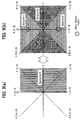
- FIGs. 7(a) and 7(b) illustrate the operation of the first decision unit 105 in the differential demodulator 100 according to the first embodiment.
- the received signal R ( m ) is a DQPSK signal
- the first difference signal Q 1 ( m ) is output when the difference signal Q( m ) is 0 and when the difference signal Q( m ) is 4, as shown in FIG. 6 .
- FIG. 6 illustrates the difference signal Q 1 ( m ) when the difference signal Q( m ) is 0 and when the difference signal Q( m ) is 4, as shown in FIG. 6 .
- the first decision unit 105 may output '0', representing the ideal signal point of phase 0 (that is, Z ( m ) 0 ) , as the first decision signal X 1 ( m )
- the first decision unit 105 may output '2', representing the ideal signal point of phase ⁇ (that is, Z ( m ) - 2), as the first decision signal X 1 ( m ) .
- the received signal R(m) is input to the received signal delay unit 106 and multiply-add operation unit 107.
- the input received signal R(m) is preferably held in D-flip-flops, a memory, or the like and the delayed received signal R(m - 1) that was held previously is output simultaneously.
- the interval of time during which the input received signal R(m) is held is preferably equal in value to the reception cycle of the received signal R ( m ) .
- the multiply-add operation unit 107 performs a multiply-add operation with reference to the received signal R ( m ) and the delayed received signal R(m - 1) and outputs the result of the multiply-add operation as a multiply-add output signal P ( m ).
- the multiply-add operation unit 107 may output, as the multiply-add output signal P ( m ), a value obtained by subtracting the result of a multiplication operation performed on the real part of the received signal R ( m ) and the imaginary part of the delayed received signal R(m - 1) from the result of a multiplication operation performed on the imaginary part of the received signal R ( m ) and the real part of the delayed received signal R(m - 1).
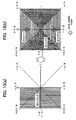
- FIG. 8 is a block diagram schematically showing the configuration of the multiply-add operation unit 107 in the differential demodulator 100 according to the first embodiment.
- the multiply-add operation unit 107 has a make-break unit 71, a first element separation unit 72, a second element separation unit 73, a first multiplication unit 74, a second multiplication unit 75, and a subtraction unit 76.
- FIG. 8 also shows that in the multiply-add operation unit 107, the received signal R ( m ) and delayed received signal R(m - 1) are both first input to the make-break unit 71.
- the make-break unit 71 outputs the received signal R ( m ) as a received internal signal r(m), and simultaneously outputs the delayed received signal R(m - 1) as a delayed received internal signal r(m - 1).
- the make-break unit 71 may simultaneously halt the output of the received internal signal r(m) and delayed received internal signal r ( m - 1). If the received signal R(m) is a DQPSK signal, for example, then as can be understood from FIG. 6 , the second difference signal Q 2 ( m ) is output from the switching unit 104 when the difference signal Q ( m ) is 1, when the difference signal Q ( m ) is 2, or when the difference signal Q ( m ) is 3.
- the received internal signal r ( m ) is input to the first element separation unit 72 and separated into a real part r i ( m ) and an imaginary part r q ( m ) .
- the delayed received internal signal r(m - 1) is input to the second element separation unit 73 and separated into a real part r i ( m - 1) and an imaginary part r q ( m - 1) .
- the first element separation unit 72 and second element separation unit 73 may have the same configuration. Alternatively, if circuits or computations can be shared by time division or the like, the functions of the first element separation unit 72 and second element separation unit 73 may be implemented by use of a single element separation unit. The processing performed by the first element separation unit 72 and second element separation unit 73 may be omitted if the received internal signal r ( m ) and delayed received internal signal r ( m - 1) are already separated into a real part and an imaginary part.
- first multiplication unit 74 in the multiply-add operation unit 107 a multiplication process is carried out on the real part r i ( m - 1) and imaginary part r q ( m ) and the result of the multiplication process is output as a first multiplication signal r i q1 ( m ) .
- second multiplication unit 75 a multiplication process is carried out on the real part r i ( m ) and imaginary part rq ( m - 1) and the result of the multiplication process is output as a second multiplication signal r i q2 (m) .
- the first multiplication unit 74 and second multiplication unit 75 may have the same configuration. Alternatively, if circuits or computations can be shared by time division or the like, the functions of the first multiplication unit 74 and second multiplication unit 75 may be implemented by use of a single multiplication unit.
- the subtraction unit 76 last carries out a subtraction signal process in which the second multiplication signal riq2(m) is subtracted from the first multiplication signal r i q 1 ( m ) and outputs the result of the subtraction signal process as a multiply-add output signal P ( m ).
- the make-break unit 71 outputs the received signal R ( m ) and delayed received signal R(m - 1) as a received internal signal r(m) and a delayed received internal signal r(m - 1) only when the second difference signal Q 2 ( m ) is output.
- the multiply- add operation unit 107 is configured to carry out the calculation in equation (2) with reference to the real part r i ( m ) and imaginary part r q ( m ) of the received internal signal r ( m ) and the real part r i ( m - 1) and imaginary part r q ( m - 1) of the delayed received internal signal r ( m - 1), the multiply-add operation unit 107 is not restricted to the configuration described above.
- P m r i m ⁇ 1 ⁇ r q m ⁇ r i m ⁇ r q m ⁇ 1
- the multiply-add output signal P ( m ) output as described above is input to the second decision unit 108.
- the second decision unit 108 outputs a second decision signal X 2 ( m ) corresponding to the magnitudes of the second difference signal Q 2 ( m ) and the multiply-add output signal P(m).
- the second decision unit 108 may select, from among the constellation of ideal signal points of the modulated signal, an ideal signal point corresponding to the result of comparisons of the value of the second difference signal Q 2 ( m ) and the value of the multiply-add output signal P ( m ) with at least one prescribed threshold value T , and output the value of the selected ideal signal point as the second decision signal X 2 ( m ). Specific examples of the operation of the second decision unit 108 will be described below.
- the second decision unit 108 preferably operates only when the second difference signal Q 2 ( m ) is output from the switching unit 104.
- the switching unit 104 outputs the second difference signal Q 2 ( m ) when the difference signal Q ( m ) is 1, when the difference signal Q ( m ) is 2, or when the difference signal Q ( m ) is 3, as can be understood from FIG. 6 .
- FIGs. 9(a) and 9(b) illustrate the operation of the second decision unit 108 in the differential demodulator 100 according to the first embodiment.
- the phase range W is the range from - ⁇ /2 to + ⁇ /2, so when expressed on the phase plane, this region appears as the vertically hatched region in FIG. 9(a) .
- the phases of the points corresponding to the four ideal signal points in the DQPSK signal constellation are assumed to be 0, ⁇ / 2, ⁇ , and 3 ⁇ /2, the ranges in which the demodulated signal points corresponding to these ideal signal points may reside are as shown in FIG. 9(b) .
- FIG. 10 illustrates the operation of the second decision unit 108 in the differential demodulator 100 according to the first embodiment.
- the received signal is assumed to be received while the receiver equipped with the differential demodulator 100 is not moving (e.g., when a vehicle in which the receiver is mounted is in a stopped state or the like)
- the received signal R(m) is assumed to have unvarying unity amplitude, and the amplitude is assumed to be 1
- the phase difference between the received signal R(m) and the delayed received signal R(m - 1) which is the phase difference of the demodulated signal, is related to the value of the multiply-add output signal P ( m ) as shown in FIG. 10 . From FIG. 10 it can be seen that:
- FIGs. 11(a) and 11(b) illustrate the operation of the second decision unit 108 in the differential demodulator 100 according to the first embodiment.
- Q 2 ( m ) 2
- the phase range W is the range from ⁇ ⁇ /4 to ⁇ 3 ⁇ /4 (with identical signs), so when expressed on the phase plane, this region appears as the vertically hatched region in FIG. 11(a) .
- the phases of the four ideal signal points in the DQPSK signal constellation are assumed to be 0, ⁇ /2 , ⁇ , and 3 ⁇ /2, the regions that can be occupied by the demodulated signal points corresponding to these ideal signal points are as shown in FIG. 11(b) .
- FIG. 12 illustrates the operation of the second decision unit 108 in the differential demodulator 100 according to the first embodiment.
- the received signal is assumed to be received while the receiver equipped with the differential demodulator 100 is not moving (e.g., when a vehicle in which the receiver is mounted is in a stopped state or the like)
- the received signal R ( m ) is assumed to have unvarying unity amplitude, and the amplitude is assumed to be 1
- the phase difference between the received signal R ( m ) and the delayed received signal R ( m - 1) which is the phase difference of the demodulated signal, is related to the value of the multiply-add output signal P ( m ) as shown in FIG. 12 . From FIG. 12 it can be seen that:
- FIGs. 13(a) and 13(b) illustrate the operation of the second decision unit 108 in the differential demodulator 100 according to the first embodiment.
- Q 2 ( m ) 3
- the phase range W is the range from ⁇ ⁇ /2 to ⁇ ⁇ (with identical signs), so when expressed on the phase plane, this region appears as the vertically hatched region in FIG. 13(a) .
- the phases of the four ideal signal points in the DQPSK signal constellation are assumed to be 0, ⁇ /2, ⁇ , and 3 ⁇ /2, the regions that can be occupied by the demodulated signal points corresponding to these ideal signal points are as shown in FIG. 13(b) .
- FIG. 14 illustrates the operation of the second decision unit 108 in the differential demodulator 100 according to the first embodiment.
- the received signal is assumed to be received while the receiver equipped with the differential demodulator 100 is not moving (e.g., when a vehicle in which the receiver is mounted is in a stopped state or the like)
- the received signal R(m) is assumed to have unvarying unity amplitude, and the amplitude is assumed to be 1
- the phase difference between the received signal R(m) and the delayed received signal R(m - 1) which is the phase difference of the demodulated signal, is related to the value of the multiply-add output signal P ( m ) as shown in FIG. 14 . From FIG. 14 it can be seen that:
- the first decision signal X 1 ( m ) and second decision signal X 2 ( m ) obtained by the above processing are input to the selection unit 109.
- the selection unit 109 On the basis of the selection signal C ( m ), the selection unit 109 outputs either the first decision signal X 1 ( m ) or the second decision signal X 2 ( m ) as the demodulated signal Z(m).
- the selection unit 109 outputs the first decision signal X 1 ( m ) as the demodulated signal Z ( m ) when the selection signal C ( m ) is '1' and the second decision signal X 2 ( m ) as the demodulated signal Z(m) when the selection signal C ( m ) is '0'.
- a region in which the received signal resides in the phase plane (one of the vertically hatched regions in FIG. 7(a) , 9(a) , 11(a) , or 13(a) ) can be identified before demodulation, and the minimal computational procedure necessary for demodulation can be singled out in advance, with the effect that the amounts of circuitry and computation necessary for the differential demodulation process can be reduced.
- FIG. 15 is a block diagram schematically showing the configuration of a differential demodulator 200 according to a second embodiment of the invention.
- This differential demodulator 200 is a device capable of carrying out the differential demodulation method according to the second embodiment.
- Component elements in FIG. 15 that are identical to or correspond to component elements of the differential demodulator 100 according to the first embodiment shown in FIG. 1 have the same reference characters as shown in FIG. 1 .
- the second embodiment differs from the first embodiment in the following three points.
- the amplitude adjustment unit 201 in FIG. 15 has the function of adjusting the amplitude of the received signal R(m) to a fixed value or a value within a fixed range and outputting the result of this adjustment as the normalized received signal A ( m ).
- the amplitude adjustment unit 201 may be configured to have an automatic gain control function, or a function that employs a bit shift operation to widen or narrow the amplitude.
- the received signal delay unit 206 in FIG. 15 has different input and output signals from the received signal delay unit 106 in the first embodiment shown in FIG. 1 , but the same configuration may be used as for the received signal delay unit 106 in the first embodiment shown in FIG. 1 .
- the multiply-add operation unit 207 has different input and output signals from the multiply-add operation unit 107 in the first embodiment shown in FIG. 1 , but the same configuration may be used as for the multiply-add operation unit 107 in the first embodiment shown in FIG. 1 .
- the differential demodulator 200 and differential demodulation method according to the second embodiment can stabilize the amplitude of the received signal.
- a region in which the received signal resides in the phase plane (one of the vertically hatched regions in FIG. 7(a) , 9(a) , 11(a) , or 13(a) ) can be identified before demodulation, and the minimal computational procedure necessary for demodulation can be singled out in advance, with the effect that the amounts of circuitry and computation necessary for the differential demodulation process can be reduced.
- FIG. 16 is a block diagram schematically showing the configuration of a differential demodulator 300 according to a third embodiment of the invention.
- This differential demodulator 300 is a device capable of carrying out the differential demodulation method according to the third embodiment.
- Component elements in FIG. 16 that are identical to or correspond to component elements of the differential demodulator 200 according to the second embodiment shown in FIG. 15 have the same reference characters as shown in FIG. 15 .
- the third embodiment differs from the second embodiment in the following three points, and is identical to the second embodiment in regard to other points.
- the amplitude adjustment unit 301 in FIG. 16 has the function of carrying out a normalization process that adjusts the amplitude of the received signal R ( m ) to a fixed value or a value within a fixed range, and outputting the result of this adjustment as the normalized received signal A ( m ).
- the amplitude adjustment unit 301 may be configured to have an automatic gain control function, or a function that employs a bit shift operation to widen or narrow the amplitude.
- the amplitude adjustment unit 301 can also output information concerning the amplitude of the output normalized received signal A ( m ) as the amplitude information signal ⁇ ( m ).
- the amplitude adjustment unit 301 may also refer to the amplitude control signal ⁇ ( m ). More specifically, the amplitude information signal ⁇ ( m ) and amplitude control signal ⁇ ( m ) are preferably control values used in automatic gain control or the number of sign bits used in the bit shift operation.
- the amplitude control unit 302 in FIG. 16 has the function of controlling amplitude information on the basis of the amplitude information signal ⁇ ( m ), and outputting the result as the amplitude control signal ⁇ ( m ) and the threshold value control signal ⁇ ( m ).
- the amplitude information signal ⁇ ( m ) is preferably a control value in automatic gain control; when the control value is the value indicating the maximum permissible amplitude or a value close to that value, a control value that reduces the amplitude can be output as the amplitude control signal ⁇ ( m ), and when the control value is the value indicating the minimum permissible amplitude or a value close to that value, a control value that increases the amplitude can be output as the amplitude control signal ⁇ ( m ).
- the amplitude information signal ⁇ ( m ) is preferably the number of sign bits in the bit shift operation; when the control value is the value indicating the minimum permissible number of sign bits or a value close to that value, a control value that reduces the amplitude can be output as the amplitude control signal ⁇ ( m ), and when the control value is the value indicating the maximum permissible number of sign bits or a value close to that value, a control value that increases the amplitude can be output as the amplitude control signal ⁇ ( m ).
- the amplitude control unit 302 may also vary the value of the threshold value control signal ⁇ ( m ) according to the magnitude of the amplitude control signal ⁇ ( m ). More specifically, when the amplitude control signal ⁇ ( m ) is a control value that reduces the amplitude, the amplitude control unit 302 may also reduce the threshold value control signal y(m). When the amplitude control signal ⁇ ( m ) is a control value that increases the amplitude, the amplitude control unit 302 may also increase the threshold value control signal ⁇ ( m ) .
- the second decision unit 308 may also be implemented by replacing the input signals of the second decision unit 108 in FIG. 15 as shown in FIG. 16 , and being configured to vary all the threshold values T according to the value of the threshold value control signal ⁇ ( m ) . More specifically, the second decision unit 308 is preferably configured to use the value of the threshold value control signal ⁇ ( m ) as a multiplier of all the threshold values T, giving them new values of ⁇ ( m ) x T. This is a method of optimizing the number of bits representing the signals by linking the threshold values used for decision purposes in the second decision unit 108 with the adjusted amplitude level (the received signal level after normalization).
- the number of bits used to represent the received signal can be set to an appropriate value or range.
- a region in which the received signal resides in the phase plane (one of the vertically hatched regions in FIG. 7(a) , 9(a) , 11(a) , or 13(a) ) can be identified before demodulation, and the minimal computational procedure necessary for demodulation can be singled out in advance, with the effect that the amounts of circuitry and computation necessary for the differential demodulation process can be reduced.
- FIG. 17 is a block diagram schematically showing the configuration of a differential demodulator 400 according to a fourth embodiment of the invention.
- This differential demodulator 400 is a device capable of carrying out the differential demodulation method according to the fourth embodiment.
- Component elements in FIG. 17 that are identical to or correspond to component elements of the differential demodulator 100 according to the first embodiment shown in FIG. 1 have the same reference characters as shown in FIG. 1 .
- the fourth embodiment differs from the first embodiment in the following three points, and is identical to the first embodiment in regard to other points.
- the multiplicity discrimination unit 410 determines the modulation multiplicity of the modulation method applied to the received signal R(m) from the input format discrimination signal H(j), and outputs the result of this determination as the modulation multiplicity signal N(j). More specifically, when the format discrimination signal H(j) is a discrimination signal representing a DQPSK signal, since the constellation of ideal signal points of the modulated signal has four points, the multiplicity discrimination unit 410 may output the modulation multiplicity signal N(j) as '4'. When the format discrimination signal H(j) is itself the modulation multiplicity of the demodulated signal, the multiplicity discrimination unit 410 may output the format discrimination signal H(j) itself as the modulation multiplicity signal N ( j ) .
- the region discrimination unit 401, comparison unit 403, switching unit 404, first decision unit 405, and second decision unit 408 make use of the modulation multiplicity in their signal processing, they can refer to the modulation multiplicity signal N ( j ). More specifically, operations in which the modulation multiplicity N used in the description of the differential demodulator 100 according to the first embodiment is replaced by the modulation multiplicity signal N ( j ) may be executed in the differential demodulator 400 and differential demodulation method according to the fourth embodiment.
- the differential demodulator 400 and differential demodulation method according to the fourth embodiment can identify a region in which the received signal resides in the phase plane (one of the vertically hatched regions in FIG. 7(a) , 9(a) , 11(a) , or 13(a) ) before demodulation, and single out in advance the minimal computational procedure necessary for demodulation, with the effect that the amounts of circuitry and computation necessary for the differential demodulation process can be reduced.
- FIG. 18 is a block diagram schematically showing the configuration of a differential demodulator 500 according to a fifth embodiment of the invention.
- the differential demodulator 500 is a device capable of carrying out the differential demodulation method according to the fifth embodiment.
- Component elements in FIG. 18 that are identical to or correspond to component elements of the differential demodulator 400 according to the fourth embodiment shown in FIG. 17 have the same reference characters as shown in FIG. 17 .
- the fifth embodiment differs from the fourth embodiment in the following two points, and is identical to the fourth embodiment in regard to other points.
- the multiplicity discrimination unit 510 in FIG. 18 determines the modulation multiplicity of the differential phase shift keying modulation method applied to the received signal R(m) and outputs the result of this determination as the modulation multiplicity signal N ( j ). More specifically, when the received signal R(m) is a DQPSK signal, for example, since there are four points in the constellation of ideal signal points of the modulated signal, the multiplicity discrimination unit 510 can output the modulation multiplicity signal N(j) as '4'.
- the multiplicity discrimination unit 510 may determine the modulation multiplicity of the differential phase shift keying modulation method applied to the received signal R(m) by, for example, cumulatively summing the received signal R(m) in the phase plane and estimating the number of convergent points obtained as the result of cumulative summation.
- the differential demodulator 500 and differential demodulation method according to the fifth embodiment can identify a region in which the received signal resides in the phase plane (one of the vertically hatched regions in FIG. 7(a) , 9(a) , 11(a) , or 13(a) ) before demodulation.
- the differential demodulator 500 and differential demodulation method according to the fifth embodiment can accordingly single out in advance the minimal computational procedure necessary for demodulation, with the effect that the amounts of circuitry and computation necessary for the differential demodulation process can be reduced.
- differential demodulators and differential demodulation methods illustrate exemplary applications of the present invention, but the invention is not limited to these examples.
- the invention may be carried out by combining component elements or processes in two or more of the first to fifth embodiments described above.
- a differential demodulator may be provided with both the amplitude adjustment unit 201 or 301 in the second or third embodiment, and the multiplicity discrimination unit 410 or 510 in the fourth or fifth embodiment.
- differential demodulators and differential demodulation methods according to the first to fifth embodiments have been described above for the case in which the DQPSK format is used as an exemplary differential phase shift keying modulation format, but the present invention can also be applied to devices and methods using differential phase shift keying modulation formats other than the DQPSK format.
- differential demodulators and differential demodulation methods according to the first to fifth embodiments described above can be applied to signal processing circuits or signal processing processes in a digital signal processor (DSP) or various other types of large scale integration (LSI) devices, including devices implemented in a field-programmable gate array (FPGA).
- DSP digital signal processor
- LSI large scale integration
- FPGA field-programmable gate array
Landscapes
- Engineering & Computer Science (AREA)
- Computer Networks & Wireless Communication (AREA)
- Signal Processing (AREA)
- Digital Transmission Methods That Use Modulated Carrier Waves (AREA)
Claims (10)
- Differentieller Demodulator (100) zum Demodulieren eines modulierten Signals, das unter Verwendung eines differentiellen Phasenverschiebungs-Modulationsverfahrens moduliert wurde, wobei der differentielle Demodulator umfasst:eine Bereichsunterscheidungseinheit (101) zum Auswählen eines Aufenthaltsbereichs, wobei es sich um einen Phasenbereich handelt, in dem sich ein empfangenes Signal in einer Phasenebene aufhält, unter einer Vielzahl von Phasenbereichen, die gemäß einer Modulations-Multiplizität des modulierten Signals unterteilt werden, und zum Ausgeben eines Unterscheidungssignals entsprechend dem Aufenthaltsbereich;eine Unterscheidungssignal-Verzögerungseinheit (102) zum Ausgeben, als ein verzögertes Unterscheidungssignal, eines Signals, das erhalten wird durch zeitliches Verzögern des Unterscheidungssignals, das von der Bereichsunterscheidungseinheit (101) ausgegeben wird;eine Vergleichseinheit (103) zum Ausgeben, als ein Differenzsignal, eines Werts entsprechend einer Differenz zwischen dem von der Bereichsunterscheidungseinheit (101) ausgegebenen Unterscheidungssignal und dem von der Unterscheidungssignal-Verzögerungseinheit (102) ausgegebenen verzögerten Unterscheidungssignal;eine Schalteinheit (104) zum Ausgeben entweder des Differenzsignals, ausgegeben von der Vergleichseinheit (103) als ein erstes Differenzsignal (Q1(m)), zusammen mit einem Auswahlsignal (C(m)) assoziiert mit dem ersten Differenzsignal, wenn der Wert des Differenzsignals, das ausgegeben wird von der Vergleichseinheit (103), in einem ersten Satz (G1) von Differenzsignalen enthalten ist, die eine vorbestimmte Bedingung erfüllen, oder zum Ausgeben des Differenzsignals als ein zweites Differenzsignal (Q2(m)), zusammen mit einem Auswahlsignal (C(m)) assoziiert mit dem zweiten Differenzsignal, wenn der Wert des Differenzsignals, das ausgegeben wird von der Vergleichseinheit (103) in einem zweiten Satz (G2) von Differenzsignalen, die nicht zu dem ersten Satz gehören, enthalten ist;eine erste Entscheidungseinheit (105) zum Ausgeben, wenn die Schalteinheit (104) das erste Differenzsignal (Q1(m)) ausgibt, eines ersten Entscheidungssignals (X1(m)) entsprechend einer Größe des ersten Differenzsignals, das ausgegeben wird von der Schalteinheit (104);eine Empfangssignal-Verzögerungseinheit (106) zum Ausgeben, als ein verzögertes Empfangssignal (R(m-1)), eines Signals, das erhalten wird durch zeitliches Verzögern des empfangenen Signals (R(m));eine Multiplikations-Additions-Betriebseinheit (107) zum Durchführen, wenn die Schalteinheit (104) das zweite Differenzsignal (Q2(m)) ausgibt, eines Multiplikations-Additions-Betriebs mit Bezug auf das empfangene Signal (R(m)) und des verzögerten Empfangssignals (R(m-1)), ausgegeben von der Empfangssignal-Verzögerungseinheit (106), und zum Ausgeben eines Resultats des Multiplikations-Additions-Betriebs als ein Multiplikations-Additions-Ausgangssignal (P(m));eine zweite Entscheidungseinheit (108) zum Ausgeben, wenn die Schalteinheit (104) das zweite Differenzsignal (Q2(m)) ausgibt, eines zweiten Entscheidungssignals (X2(m)) entsprechend einer Größe des zweiten Differenzsignals, ausgegeben von der Schalteinheit (104), und einer Größe des Multiplikations-Additions-Ausgangssignals, ausgegeben von der Multiplikations-Additions-Betriebseinheit (107); undeine Auswahleinheit (109) zum Auswählen eines einzelnen Signals aus dem ersten Entscheidungssignal und dem zweiten Entscheidungssignal auf Grundlage des Auswahlsignals (C(m)), ausgegeben von der Schalteinheit (104), und zum Ausgeben des ausgewählten einzelnen Signals als ein demoduliertes Signal (Z(m)); wobeider erste Satz (G1) ein Satz der Differenzsignale ist, so dass eine totale Größe der Phasenbereiche in der Phasenebene entsprechend den Differenzsignalen gleich zu oder geringer als eine Phasendifferenz zwischen den idealen Signalpunkten ist, in einer Konstellation von idealen Signalpunkten des modulierten Signals, die in der Phasenebene benachbart sind;wobei das empfangene Signal und das verzögerte empfangene Signal beide komplexe Zahlen sind; unddie Multiplikations-Additions-Betriebseinheit (107) einen Multiplikationsbetrieb an einem imaginären Teil des empfangenen Signals und einem realen Teil des verzögerten empfangenen Signals durchführt, einen Multiplikationsbetrieb an einem realen Teil des empfangenen Signals und einem imaginären Teil des verzögerten empfangenen Signals durchführt, und einen Subtraktionsbetrieb an zwei realen Zahlen durchführt, um das Multiplikations-Additions-Ausgangssignal zu erzeugen.
- Differential-Demodulator (200) nach Anspruch 1, ferner mit einer Amplitudenanpassungseinheit (201) zum Normalisieren des empfangenen Signals, das erhalten wird durch Steuern einer Amplitude des empfangenen Signals, zum Halten der Amplitude auf einem festen Wert oder innerhalb eines festen Bereichs, und zum Ausgeben des normalisierten empfangenen Signals, wobei:das verzögerte empfangene Signal, ausgegeben durch die Empfangssignal-Verzögerungseinheit (206), ein Signal ist, das erhalten wird durch temporäres Verzögern des normalisierten empfangenen Signals, ausgegeben von der Amplitudenanpassungseinheit (201); unddas Multiplikations-Additions-Ausgangssignal, ausgegeben durch die Multiplikations-Additions-Betriebseinheit (207), ein Signal ist basierend auf einem Resultat eines Multiplikations-Additions-Betriebs, der durchgeführt wird mit Bezug auf den Wert des normalisierten empfangenen Signals und dem Wert des normalisierten verzögerten empfangenen Signals.
- Differential-Demodulator (400) nach Anspruch 1, ferner mit einer Multiplizitäts-Unterscheidungseinheit (410) zum Unterscheiden der Modulations-Multiplizität mit Bezug auf eine Information betreffend des differentiellen PhasenverschiebungsModulationsverfahrens, und zum Ausgeben eines Werts der Modulations-Multiplizität als ein Modulations-Multiplizitätssignal, wobei:die Bereichsunterscheidungseinheit (401) den Aufenthaltsbereich auswählt, wobei es sich um den Phasenbereich handelt, in dem sich das empfangene Signal in der Phasenebene aufhält, unter einer Vielzahl von Phasenbereichen, die gemäß dem Modulations-Multiplizitätssignal unterschieden werden, und das Unterscheidungssignal entsprechend dem Aufenthaltsbereich ausgibt; unddie Vergleichseinheit (403), als das Differenzsignal,einen Wert ausgibt, der eindeutig durch das Modulations-Multiplizitätssignal und der Differenz zwischen dem Unterscheidungssignal und dem verzögerten Unterscheidungssignal bestimmt wird.
- Differential-Demodulator (500) nach Anspruch 1, ferner mit einer Multiplizitäts-Unterscheidungseinheit (510) zum Unterscheiden der Modulations-Multiplizität mit Bezug auf das empfangene Signal, und zum Ausgeben eines Werts der Modulations-Multiplizität als ein Modulations-Multiplizitätssignal, wobei:die Bereichsunterscheidungseinheit (401) den Aufenthaltsbereich auswählt, wobei es sich um den Phasenbereich handelt, in dem sich das empfangene Signal in der Phasenebene aufhält, unter einer Vielzahl von Phasenbereichen, die gemäß dem Modulations-Multiplizitätssignal unterschieden werden, und das Unterscheidungssignal entsprechend dem Aufenthaltsbereich ausgibt; unddie Vergleichseinheit (403), als das Differenzsignal, einen Wert ausgibt, der eindeutig gemäß dem Modulations-Multiplizitätssignal und der Differenz zwischen dem Unterscheidungssignal und dem verzögerten Unterscheidungssignal bestimmt ist.
- Differential-Demodulator (100) nach einem der Ansprüche 1-4, wobei die Vielzahl von Phasenbereichen Bereiche sind, die erhalten werden durch Unterteilen der Phasenebene bei gleichen Phasenintervallen, wobei Werte, die entgegen dem Uhrzeigersinn anwachsen und auf eine Phase 0 Bezug nehmen, zu jedem der Vielzahl von Phasenbereiche als das Unterscheidungssignal hinzugefügt sind, und die Vergleichseinheit (103) die Differenz zwischen dem Unterscheidungssignal und dem verzögerten Unterscheidungssignal als das Differenzsignal ausgibt.
- Differential-Demodulator (100) nach Anspruch 5, wobei die Anzahl von Bereichen in der Vielzahl von Phasenbereichen zwei Mal die Modulations-Multiplizität des modulierten Signals ist.
- Differential-Demodulator (100) nach einem der Ansprüche 1-6, wobei die Multiplikations-Additions-Betriebseinheit (107) als das Multiplikations-Additions-Ausgangssignal einen Wert ausgibt, der erhalten wird durch Subtrahieren eines Resultats einer Multiplikation des realen Teils des empfangenen Signals mit dem imaginären Teil des verzögerten empfangenen Signals von einem Resultat einer Multiplikation des imaginären Teils des empfangenen Signals mit dem realen Teil des verzögerten empfangenen Signals.
- Differential-Demodulator (100) nach einem der Ansprüche 1-7, wobei:die erste Entscheidungseinheit (105) einen idealen Signalpunkt entsprechend einem Wert des ersten Entscheidungssignals unter der Konstellation von idealen Signalpunkten des modulierten Signals auswählt, und einen Wert des ausgewählten idealen Signalpunkts als das erste Entscheidungssignal ausgibt; unddie zweite Entscheidungseinheit (108), unter der Konstellation von idealen Signalpunkten des modulierten Signals, einen idealen Signalpunkt entsprechend einem Resultat eines Vergleichs des Werts des zweiten Differenzsignals und dem Wert des Multiplikations-Additions-Ausgangssignals mit zumindest einem vorgegebenen Schwellenwert auswählt, und einen Wert des ausgewählten idealen Signalpunkts als das zweite Entscheidungssignal ausgibt.
- Differential-Demodulator (300) nach Anspruch 2, ferner mit einer Amplitudensteuereinheit (302) zum Bezugnehmen auf, als ein Amplitudeninformationssignal, eine Information betreffend die Amplitude des normalisierten empfangenen Signals, und zum Ausgeben eines Amplitudensteuersignals und eines Schwellenwertsteuersignals, wobei:die Amplitudenanpassungseinheit (301) das Amplitudeninformationssignal sowie das normalisierte empfangene Signal, erhalten unter Verwendung des Amplitudensteuersignals zum Normalisieren des empfangenen Signals, dessen Amplitude bei dem festen Wert oder innerhalb des festen Bereichs gesteuert wurde, ausgibt; unddie zweite Entscheidungseinheit (308) einen idealen Signalpunkt entsprechend einem Resultat eines Vergleichs des Werts des zweiten Differenzsignals und dem Wert des Multiplikations-Additions-Ausgangssignals mit zumindest einem vorgegebenen Schwellenwert basierend auf dem Schwellenwertsteuersignal auswählt, unter der Konstellation von idealen Signalpunkten des modulierten Signals, und einen Wert des ausgewählten idealen Signalpunkts als das zweite Entscheidungssignal ausgibt.
- Differential-Demodulationsverfahren zum Demodulieren eines modulierten Signals, das unter Verwendung eines differentiellen Phasenverschiebungsmodulationsverfahrens moduliert wurde, wobei das Differential-Demodulationsverfahren umfasst:Auswählen eines Aufenthaltsbereichs, wobei es sich um einen Phasenbereich handelt, in dem sich ein empfangenes Signal in einer Phasenebene aufhält, unter einer Vielzahl von Phasenbereichen, die unterteilt werden gemäß einer Modulations-Multiplizität des modulierten Signals, und Erzeugen eines Entscheidungssignals entsprechend dem Aufenthaltsbereich;Erzeugen, als ein verzögertes Unterscheidungssignal, eines Signals, das erhalten wird durch temporäres Verzögern des Unterscheidungssignals;Erzeugen, als ein Differenzsignal, eines Werts entsprechend einer Differenz zwischen dem Unterscheidungssignal und dem verzögerten Unterscheidungssignal;entweder Ausgeben des Differenzsignals als ein erstes Differenzsignal (Q1(m)), zusammen mit einem Auswahlsignal (C(m)) assoziiert mit dem ersten Differenzsignal, wenn der Wert des Differenzsignals in einem ersten Satz (G1) von Differenzsignalen enthalten ist, die eine vorbestimmte Bedingung erfüllen, oder Ausgeben des Differenzsignals als ein zweites Differenzsignal (Q2(m)), zusammen mit einem Auswahlsignal (C(m)) assoziiert mit dem zweiten Differenzsignal, wenn der Wert des Differenzsignals in einem zweiten Satz (G2) von Differenzsignalausgaben, die nicht zu dem ersten Satz gehören, enthalten ist;Ausgeben, wenn die Schalteinheit (104) das erste Differenzsignal (Q1(m)) ausgibt, eines ersten Entscheidungssignals (X1(m)) entsprechend einer Größe des ersten Differenzsignals;Ausgeben, als ein verzögertes empfangenes Signal (R(m-1)), eines Signals, das erhalten wird durch temporäres Verzögern des empfangenen Signals (R(m));Durchführen, wenn die Schalteinheit (104) das zweite Differenzsignal (Q2(m)) ausgibt, eines Multiplikations-Additions-Betriebs mit Bezug auf das empfangene Signal (R(m)) und des verzögerten empfangenen Signals (R(m-1)), und Ausgeben eines Resultats des Multiplikations-Additions-Betriebs als ein Multiplikations-Additions-Ausgangssignal (P(m));Ausgeben, wenn die Schalteinheit (104) das zweite Differenzsignal (Q2(m)) ausgibt, eines zweiten Entscheidungssignals (X2(m)) entsprechend einer Größe des zweiten Differenzsignals und einer Größe des Multiplikations-Additions-Ausgangssignals; undAuswählen eines einzelnen Signals unter dem ersten Entscheidungssignal und dem zweiten Entscheidungssignal auf Grundlage des Auswahlsignals, und Ausgeben des ausgewählten einzelnen Signals als ein demoduliertes Signal; wobeider erste Satz ein Satz der Differenzsignale ist, so dass eine totale Größe der Phasenbereiche in der Phasenebene entsprechend den Differenzsignalen gleich zu oder geringer als eine Phasendifferenz zwischen idealen Signalpunkten ist, in der Konstellation idealer Signalpunkte des modulierten Signals, die in der Phasenebene benachbart sind;das empfangene Signal und das verzögerte empfangene Signal beide komplexe Zahlen sind; undDurchführen eines Multiplikations-Additions-Betriebs ferner ein Durchführen eines Multiplikations-Betriebs an einem imaginären Teil des empfangenen Signals und einem realen Teil des verzögerten empfangenen Signals umfasst, Durchführen eines Multiplikations-Betriebs an einem realen Teil des empfangenen Signals und einem imaginären Teil des verzögerten empfangenen Signals, und Erzeugen des Multiplikations-Additions-Ausgangssignals durch Durchführen eines Subtraktionsbetriebs an zwei realen Zahlen zum Erzeugen des Multiplikations-Additions-Ausgangssignals.
Applications Claiming Priority (1)
| Application Number | Priority Date | Filing Date | Title |
|---|---|---|---|
| JP2014080870A JP6214454B2 (ja) | 2014-04-10 | 2014-04-10 | 差動復調装置及び差動復調方法 |
Publications (2)
| Publication Number | Publication Date |
|---|---|
| EP2930897A1 EP2930897A1 (de) | 2015-10-14 |
| EP2930897B1 true EP2930897B1 (de) | 2016-11-02 |
Family
ID=52785004
Family Applications (1)
| Application Number | Title | Priority Date | Filing Date |
|---|---|---|---|
| EP15162376.6A Active EP2930897B1 (de) | 2014-04-10 | 2015-04-02 | Differentielle demodulationsvorrichtung und differentielles demodulationsverfahren |
Country Status (3)
| Country | Link |
|---|---|
| EP (1) | EP2930897B1 (de) |
| JP (1) | JP6214454B2 (de) |
| CN (1) | CN104980387B (de) |
Families Citing this family (1)
| Publication number | Priority date | Publication date | Assignee | Title |
|---|---|---|---|---|
| CN108134754B (zh) * | 2018-01-09 | 2019-02-01 | 西安科技大学 | 一种吉比特连续可变速率的中频差分解调器 |
Family Cites Families (5)
| Publication number | Priority date | Publication date | Assignee | Title |
|---|---|---|---|---|
| JPH0697971A (ja) * | 1992-09-16 | 1994-04-08 | Fujitsu Ltd | 遅延検波復調器 |
| JPH09233138A (ja) * | 1996-02-22 | 1997-09-05 | Sony Corp | 情報伝送システムおよび情報受信装置、並びに情報伝送方法 |
| JP2004364131A (ja) * | 2003-06-06 | 2004-12-24 | Seiko Epson Corp | 位相変調信号復調装置及び復調方法 |
| CN1972262A (zh) * | 2005-11-25 | 2007-05-30 | 精工爱普生株式会社 | Psk接收机及其接收方法、psk解调电路和通信装置 |
| JP5599507B2 (ja) * | 2011-05-11 | 2014-10-01 | 三菱電機株式会社 | 差動復調装置及び差動復調方法 |
-
2014
- 2014-04-10 JP JP2014080870A patent/JP6214454B2/ja active Active
-
2015
- 2015-04-02 EP EP15162376.6A patent/EP2930897B1/de active Active
- 2015-04-10 CN CN201510169142.5A patent/CN104980387B/zh active Active
Also Published As
| Publication number | Publication date |
|---|---|
| JP2015201810A (ja) | 2015-11-12 |
| EP2930897A1 (de) | 2015-10-14 |
| CN104980387B (zh) | 2018-05-08 |
| JP6214454B2 (ja) | 2017-10-18 |
| CN104980387A (zh) | 2015-10-14 |
Similar Documents
| Publication | Publication Date | Title |
|---|---|---|
| EP1172956B1 (de) | OFDM Nachrichtenübertragunds-Packetempfänger | |
| EP0887976A2 (de) | Empfänger,Sendeempfänger und Kommunikationsverfahren | |
| US7139333B2 (en) | Frequency error estimating receiver, and frequency error estimating method | |
| EP1780921A1 (de) | Störsignal-detektionseinrichtung und ofdm-empfangseinrichtung damit | |
| KR100269652B1 (ko) | 에러율 추정기 | |
| EP1516469B1 (de) | Verfahren und vorrichtung zur semikohärenten phasendomänendemodulation | |
| US20090245428A1 (en) | Method and apparatus for processing communication signal | |
| KR100311263B1 (ko) | 파일롯 신호를 포함하는 수신 신호를 복조하는 방법 및 장치 | |
| JPH09247221A (ja) | 回線制御装置 | |
| EP2930897B1 (de) | Differentielle demodulationsvorrichtung und differentielles demodulationsverfahren | |
| KR19980071589A (ko) | 에러보정기능을 지닌 차동검파기 | |
| JP3789157B2 (ja) | 周波数誤差推定装置 | |
| EP1047235A1 (de) | Trägerphasenschätzer sowie demodulator | |
| JP4130831B2 (ja) | 動的dcオフセット除去装置及び動的dcオフセット除去方法 | |
| JP7660970B2 (ja) | 対数尤度比算出回路および無線受信装置 | |
| JP3899425B2 (ja) | Qpsk変調方式システムの自動周波数制御装置及びその方法 | |
| JP4257733B2 (ja) | キャリア周波数同期回路 | |
| US7609615B2 (en) | Method and apparatus for performing channel compensation and symbol demodulation for coherent demodulation in an OFDM system | |
| US20260012376A1 (en) | Signal processing apparatus | |
| JP2008124948A (ja) | 無線通信装置及び通信処理回路 | |
| JP4138701B2 (ja) | 無線通信装置及びキャリア周波数誤差補償方法 | |
| JP2000188620A (ja) | 同期検波装置 | |
| US20010024483A1 (en) | Radio reception apparatus | |
| JP2003244265A (ja) | 位相比較器 | |
| JP2004180346A (ja) | 周波数オフセット補正装置 |
Legal Events
| Date | Code | Title | Description |
|---|---|---|---|
| PUAI | Public reference made under article 153(3) epc to a published international application that has entered the european phase |
Free format text: ORIGINAL CODE: 0009012 |
|
| 17P | Request for examination filed |
Effective date: 20150402 |
|
| AK | Designated contracting states |
Kind code of ref document: A1 Designated state(s): AL AT BE BG CH CY CZ DE DK EE ES FI FR GB GR HR HU IE IS IT LI LT LU LV MC MK MT NL NO PL PT RO RS SE SI SK SM TR |
|
| AX | Request for extension of the european patent |
Extension state: BA ME |
|
| GRAP | Despatch of communication of intention to grant a patent |
Free format text: ORIGINAL CODE: EPIDOSNIGR1 |
|
| RIC1 | Information provided on ipc code assigned before grant |
Ipc: H04L 27/233 20060101AFI20160428BHEP |
|
| INTG | Intention to grant announced |
Effective date: 20160520 |
|
| GRAS | Grant fee paid |
Free format text: ORIGINAL CODE: EPIDOSNIGR3 |
|
| GRAA | (expected) grant |
Free format text: ORIGINAL CODE: 0009210 |
|
| AK | Designated contracting states |
Kind code of ref document: B1 Designated state(s): AL AT BE BG CH CY CZ DE DK EE ES FI FR GB GR HR HU IE IS IT LI LT LU LV MC MK MT NL NO PL PT RO RS SE SI SK SM TR |
|
| REG | Reference to a national code |
Ref country code: GB Ref legal event code: FG4D |
|
| REG | Reference to a national code |
Ref country code: AT Ref legal event code: REF Ref document number: 842817 Country of ref document: AT Kind code of ref document: T Effective date: 20161115 Ref country code: CH Ref legal event code: EP |
|
| REG | Reference to a national code |
Ref country code: IE Ref legal event code: FG4D |
|
| REG | Reference to a national code |
Ref country code: DE Ref legal event code: R096 Ref document number: 602015000584 Country of ref document: DE |
|
| PG25 | Lapsed in a contracting state [announced via postgrant information from national office to epo] |
Ref country code: LV Free format text: LAPSE BECAUSE OF FAILURE TO SUBMIT A TRANSLATION OF THE DESCRIPTION OR TO PAY THE FEE WITHIN THE PRESCRIBED TIME-LIMIT Effective date: 20161102 |
|
| REG | Reference to a national code |
Ref country code: NL Ref legal event code: MP Effective date: 20161102 |
|
| REG | Reference to a national code |
Ref country code: LT Ref legal event code: MG4D |
|
| REG | Reference to a national code |
Ref country code: AT Ref legal event code: MK05 Ref document number: 842817 Country of ref document: AT Kind code of ref document: T Effective date: 20161102 |
|
| PG25 | Lapsed in a contracting state [announced via postgrant information from national office to epo] |
Ref country code: SE Free format text: LAPSE BECAUSE OF FAILURE TO SUBMIT A TRANSLATION OF THE DESCRIPTION OR TO PAY THE FEE WITHIN THE PRESCRIBED TIME-LIMIT Effective date: 20161102 Ref country code: NL Free format text: LAPSE BECAUSE OF FAILURE TO SUBMIT A TRANSLATION OF THE DESCRIPTION OR TO PAY THE FEE WITHIN THE PRESCRIBED TIME-LIMIT Effective date: 20161102 Ref country code: NO Free format text: LAPSE BECAUSE OF FAILURE TO SUBMIT A TRANSLATION OF THE DESCRIPTION OR TO PAY THE FEE WITHIN THE PRESCRIBED TIME-LIMIT Effective date: 20170202 Ref country code: LT Free format text: LAPSE BECAUSE OF FAILURE TO SUBMIT A TRANSLATION OF THE DESCRIPTION OR TO PAY THE FEE WITHIN THE PRESCRIBED TIME-LIMIT Effective date: 20161102 Ref country code: GR Free format text: LAPSE BECAUSE OF FAILURE TO SUBMIT A TRANSLATION OF THE DESCRIPTION OR TO PAY THE FEE WITHIN THE PRESCRIBED TIME-LIMIT Effective date: 20170203 |
|
| PG25 | Lapsed in a contracting state [announced via postgrant information from national office to epo] |
Ref country code: IS Free format text: LAPSE BECAUSE OF FAILURE TO SUBMIT A TRANSLATION OF THE DESCRIPTION OR TO PAY THE FEE WITHIN THE PRESCRIBED TIME-LIMIT Effective date: 20170302 Ref country code: AT Free format text: LAPSE BECAUSE OF FAILURE TO SUBMIT A TRANSLATION OF THE DESCRIPTION OR TO PAY THE FEE WITHIN THE PRESCRIBED TIME-LIMIT Effective date: 20161102 Ref country code: RS Free format text: LAPSE BECAUSE OF FAILURE TO SUBMIT A TRANSLATION OF THE DESCRIPTION OR TO PAY THE FEE WITHIN THE PRESCRIBED TIME-LIMIT Effective date: 20161102 Ref country code: ES Free format text: LAPSE BECAUSE OF FAILURE TO SUBMIT A TRANSLATION OF THE DESCRIPTION OR TO PAY THE FEE WITHIN THE PRESCRIBED TIME-LIMIT Effective date: 20161102 Ref country code: HR Free format text: LAPSE BECAUSE OF FAILURE TO SUBMIT A TRANSLATION OF THE DESCRIPTION OR TO PAY THE FEE WITHIN THE PRESCRIBED TIME-LIMIT Effective date: 20161102 Ref country code: FI Free format text: LAPSE BECAUSE OF FAILURE TO SUBMIT A TRANSLATION OF THE DESCRIPTION OR TO PAY THE FEE WITHIN THE PRESCRIBED TIME-LIMIT Effective date: 20161102 Ref country code: PL Free format text: LAPSE BECAUSE OF FAILURE TO SUBMIT A TRANSLATION OF THE DESCRIPTION OR TO PAY THE FEE WITHIN THE PRESCRIBED TIME-LIMIT Effective date: 20161102 Ref country code: PT Free format text: LAPSE BECAUSE OF FAILURE TO SUBMIT A TRANSLATION OF THE DESCRIPTION OR TO PAY THE FEE WITHIN THE PRESCRIBED TIME-LIMIT Effective date: 20170302 |
|
| PG25 | Lapsed in a contracting state [announced via postgrant information from national office to epo] |
Ref country code: DK Free format text: LAPSE BECAUSE OF FAILURE TO SUBMIT A TRANSLATION OF THE DESCRIPTION OR TO PAY THE FEE WITHIN THE PRESCRIBED TIME-LIMIT Effective date: 20161102 Ref country code: CZ Free format text: LAPSE BECAUSE OF FAILURE TO SUBMIT A TRANSLATION OF THE DESCRIPTION OR TO PAY THE FEE WITHIN THE PRESCRIBED TIME-LIMIT Effective date: 20161102 Ref country code: EE Free format text: LAPSE BECAUSE OF FAILURE TO SUBMIT A TRANSLATION OF THE DESCRIPTION OR TO PAY THE FEE WITHIN THE PRESCRIBED TIME-LIMIT Effective date: 20161102 Ref country code: SK Free format text: LAPSE BECAUSE OF FAILURE TO SUBMIT A TRANSLATION OF THE DESCRIPTION OR TO PAY THE FEE WITHIN THE PRESCRIBED TIME-LIMIT Effective date: 20161102 Ref country code: RO Free format text: LAPSE BECAUSE OF FAILURE TO SUBMIT A TRANSLATION OF THE DESCRIPTION OR TO PAY THE FEE WITHIN THE PRESCRIBED TIME-LIMIT Effective date: 20161102 |
|
| REG | Reference to a national code |
Ref country code: DE Ref legal event code: R097 Ref document number: 602015000584 Country of ref document: DE |
|
| PG25 | Lapsed in a contracting state [announced via postgrant information from national office to epo] |
Ref country code: BE Free format text: LAPSE BECAUSE OF FAILURE TO SUBMIT A TRANSLATION OF THE DESCRIPTION OR TO PAY THE FEE WITHIN THE PRESCRIBED TIME-LIMIT Effective date: 20161102 Ref country code: BG Free format text: LAPSE BECAUSE OF FAILURE TO SUBMIT A TRANSLATION OF THE DESCRIPTION OR TO PAY THE FEE WITHIN THE PRESCRIBED TIME-LIMIT Effective date: 20170202 Ref country code: IT Free format text: LAPSE BECAUSE OF FAILURE TO SUBMIT A TRANSLATION OF THE DESCRIPTION OR TO PAY THE FEE WITHIN THE PRESCRIBED TIME-LIMIT Effective date: 20161102 Ref country code: SM Free format text: LAPSE BECAUSE OF FAILURE TO SUBMIT A TRANSLATION OF THE DESCRIPTION OR TO PAY THE FEE WITHIN THE PRESCRIBED TIME-LIMIT Effective date: 20161102 |
|
| PLBE | No opposition filed within time limit |
Free format text: ORIGINAL CODE: 0009261 |
|
| STAA | Information on the status of an ep patent application or granted ep patent |
Free format text: STATUS: NO OPPOSITION FILED WITHIN TIME LIMIT |
|
| 26N | No opposition filed |
Effective date: 20170803 |
|
| PG25 | Lapsed in a contracting state [announced via postgrant information from national office to epo] |
Ref country code: SI Free format text: LAPSE BECAUSE OF FAILURE TO SUBMIT A TRANSLATION OF THE DESCRIPTION OR TO PAY THE FEE WITHIN THE PRESCRIBED TIME-LIMIT Effective date: 20161102 |
|
| REG | Reference to a national code |
Ref country code: IE Ref legal event code: MM4A |
|
| REG | Reference to a national code |
Ref country code: FR Ref legal event code: ST Effective date: 20171229 |
|
| PG25 | Lapsed in a contracting state [announced via postgrant information from national office to epo] |
Ref country code: MC Free format text: LAPSE BECAUSE OF FAILURE TO SUBMIT A TRANSLATION OF THE DESCRIPTION OR TO PAY THE FEE WITHIN THE PRESCRIBED TIME-LIMIT Effective date: 20161102 Ref country code: FR Free format text: LAPSE BECAUSE OF NON-PAYMENT OF DUE FEES Effective date: 20170502 |
|
| PG25 | Lapsed in a contracting state [announced via postgrant information from national office to epo] |
Ref country code: LU Free format text: LAPSE BECAUSE OF NON-PAYMENT OF DUE FEES Effective date: 20170402 |
|
| PG25 | Lapsed in a contracting state [announced via postgrant information from national office to epo] |
Ref country code: IE Free format text: LAPSE BECAUSE OF NON-PAYMENT OF DUE FEES Effective date: 20170402 |
|
| PG25 | Lapsed in a contracting state [announced via postgrant information from national office to epo] |
Ref country code: MT Free format text: LAPSE BECAUSE OF NON-PAYMENT OF DUE FEES Effective date: 20170402 |
|
| REG | Reference to a national code |
Ref country code: CH Ref legal event code: PL |
|
| REG | Reference to a national code |
Ref country code: DE Ref legal event code: R084 Ref document number: 602015000584 Country of ref document: DE |
|
| REG | Reference to a national code |
Ref country code: GB Ref legal event code: 746 Effective date: 20190124 |
|
| PG25 | Lapsed in a contracting state [announced via postgrant information from national office to epo] |
Ref country code: CH Free format text: LAPSE BECAUSE OF NON-PAYMENT OF DUE FEES Effective date: 20180430 Ref country code: LI Free format text: LAPSE BECAUSE OF NON-PAYMENT OF DUE FEES Effective date: 20180430 |
|
| PG25 | Lapsed in a contracting state [announced via postgrant information from national office to epo] |
Ref country code: HU Free format text: LAPSE BECAUSE OF FAILURE TO SUBMIT A TRANSLATION OF THE DESCRIPTION OR TO PAY THE FEE WITHIN THE PRESCRIBED TIME-LIMIT; INVALID AB INITIO Effective date: 20150402 |
|
| PG25 | Lapsed in a contracting state [announced via postgrant information from national office to epo] |
Ref country code: CY Free format text: LAPSE BECAUSE OF FAILURE TO SUBMIT A TRANSLATION OF THE DESCRIPTION OR TO PAY THE FEE WITHIN THE PRESCRIBED TIME-LIMIT Effective date: 20161102 |
|
| PG25 | Lapsed in a contracting state [announced via postgrant information from national office to epo] |
Ref country code: MK Free format text: LAPSE BECAUSE OF FAILURE TO SUBMIT A TRANSLATION OF THE DESCRIPTION OR TO PAY THE FEE WITHIN THE PRESCRIBED TIME-LIMIT Effective date: 20161102 |
|
| PG25 | Lapsed in a contracting state [announced via postgrant information from national office to epo] |
Ref country code: TR Free format text: LAPSE BECAUSE OF FAILURE TO SUBMIT A TRANSLATION OF THE DESCRIPTION OR TO PAY THE FEE WITHIN THE PRESCRIBED TIME-LIMIT Effective date: 20161102 |
|
| PG25 | Lapsed in a contracting state [announced via postgrant information from national office to epo] |
Ref country code: AL Free format text: LAPSE BECAUSE OF FAILURE TO SUBMIT A TRANSLATION OF THE DESCRIPTION OR TO PAY THE FEE WITHIN THE PRESCRIBED TIME-LIMIT Effective date: 20161102 |
|
| P01 | Opt-out of the competence of the unified patent court (upc) registered |
Effective date: 20230512 |
|
| PGFP | Annual fee paid to national office [announced via postgrant information from national office to epo] |
Ref country code: GB Payment date: 20250227 Year of fee payment: 11 |
|
| PGFP | Annual fee paid to national office [announced via postgrant information from national office to epo] |
Ref country code: DE Payment date: 20250305 Year of fee payment: 11 |