EP0867938A2 - Halbleiteranordnung mit Elektrodenflächen und Leiter - Google Patents
Halbleiteranordnung mit Elektrodenflächen und Leiter Download PDFInfo
- Publication number
- EP0867938A2 EP0867938A2 EP97308718A EP97308718A EP0867938A2 EP 0867938 A2 EP0867938 A2 EP 0867938A2 EP 97308718 A EP97308718 A EP 97308718A EP 97308718 A EP97308718 A EP 97308718A EP 0867938 A2 EP0867938 A2 EP 0867938A2
- Authority
- EP
- European Patent Office
- Prior art keywords
- adhesive tape
- electrode pads
- insulating adhesive
- bonding wires
- insulating
- Prior art date
- Legal status (The legal status is an assumption and is not a legal conclusion. Google has not performed a legal analysis and makes no representation as to the accuracy of the status listed.)
- Withdrawn
Links
Images


Classifications
-
- H—ELECTRICITY
- H10—SEMICONDUCTOR DEVICES; ELECTRIC SOLID-STATE DEVICES NOT OTHERWISE PROVIDED FOR
- H10W—GENERIC PACKAGES, INTERCONNECTIONS, CONNECTORS OR OTHER CONSTRUCTIONAL DETAILS OF DEVICES COVERED BY CLASS H10
- H10W72/00—Interconnections or connectors in packages
- H10W72/071—Connecting or disconnecting
-
- H—ELECTRICITY
- H10—SEMICONDUCTOR DEVICES; ELECTRIC SOLID-STATE DEVICES NOT OTHERWISE PROVIDED FOR
- H10W—GENERIC PACKAGES, INTERCONNECTIONS, CONNECTORS OR OTHER CONSTRUCTIONAL DETAILS OF DEVICES COVERED BY CLASS H10
- H10W70/00—Package substrates; Interposers; Redistribution layers [RDL]
- H10W70/40—Leadframes
- H10W70/411—Chip-supporting parts, e.g. die pads
- H10W70/415—Leadframe inner leads serving as die pads
-
- H—ELECTRICITY
- H10—SEMICONDUCTOR DEVICES; ELECTRIC SOLID-STATE DEVICES NOT OTHERWISE PROVIDED FOR
- H10W—GENERIC PACKAGES, INTERCONNECTIONS, CONNECTORS OR OTHER CONSTRUCTIONAL DETAILS OF DEVICES COVERED BY CLASS H10
- H10W72/00—Interconnections or connectors in packages
- H10W72/01—Manufacture or treatment
- H10W72/019—Manufacture or treatment of bond pads
-
- H—ELECTRICITY
- H10—SEMICONDUCTOR DEVICES; ELECTRIC SOLID-STATE DEVICES NOT OTHERWISE PROVIDED FOR
- H10W—GENERIC PACKAGES, INTERCONNECTIONS, CONNECTORS OR OTHER CONSTRUCTIONAL DETAILS OF DEVICES COVERED BY CLASS H10
- H10W72/00—Interconnections or connectors in packages
- H10W72/071—Connecting or disconnecting
- H10W72/075—Connecting or disconnecting of bond wires
-
- H—ELECTRICITY
- H10—SEMICONDUCTOR DEVICES; ELECTRIC SOLID-STATE DEVICES NOT OTHERWISE PROVIDED FOR
- H10W—GENERIC PACKAGES, INTERCONNECTIONS, CONNECTORS OR OTHER CONSTRUCTIONAL DETAILS OF DEVICES COVERED BY CLASS H10
- H10W72/00—Interconnections or connectors in packages
- H10W72/90—Bond pads, in general
-
- H—ELECTRICITY
- H10—SEMICONDUCTOR DEVICES; ELECTRIC SOLID-STATE DEVICES NOT OTHERWISE PROVIDED FOR
- H10W—GENERIC PACKAGES, INTERCONNECTIONS, CONNECTORS OR OTHER CONSTRUCTIONAL DETAILS OF DEVICES COVERED BY CLASS H10
- H10W70/00—Package substrates; Interposers; Redistribution layers [RDL]
- H10W70/60—Insulating or insulated package substrates; Interposers; Redistribution layers
-
- H—ELECTRICITY
- H10—SEMICONDUCTOR DEVICES; ELECTRIC SOLID-STATE DEVICES NOT OTHERWISE PROVIDED FOR
- H10W—GENERIC PACKAGES, INTERCONNECTIONS, CONNECTORS OR OTHER CONSTRUCTIONAL DETAILS OF DEVICES COVERED BY CLASS H10
- H10W72/00—Interconnections or connectors in packages
- H10W72/071—Connecting or disconnecting
- H10W72/0711—Apparatus therefor
-
- H—ELECTRICITY
- H10—SEMICONDUCTOR DEVICES; ELECTRIC SOLID-STATE DEVICES NOT OTHERWISE PROVIDED FOR
- H10W—GENERIC PACKAGES, INTERCONNECTIONS, CONNECTORS OR OTHER CONSTRUCTIONAL DETAILS OF DEVICES COVERED BY CLASS H10
- H10W72/00—Interconnections or connectors in packages
- H10W72/20—Bump connectors, e.g. solder bumps or copper pillars; Dummy bumps; Thermal bumps
- H10W72/29—Bond pads specially adapted therefor
-
- H—ELECTRICITY
- H10—SEMICONDUCTOR DEVICES; ELECTRIC SOLID-STATE DEVICES NOT OTHERWISE PROVIDED FOR
- H10W—GENERIC PACKAGES, INTERCONNECTIONS, CONNECTORS OR OTHER CONSTRUCTIONAL DETAILS OF DEVICES COVERED BY CLASS H10
- H10W72/00—Interconnections or connectors in packages
- H10W72/50—Bond wires
- H10W72/531—Shapes of wire connectors
- H10W72/536—Shapes of wire connectors the connected ends being ball-shaped
-
- H—ELECTRICITY
- H10—SEMICONDUCTOR DEVICES; ELECTRIC SOLID-STATE DEVICES NOT OTHERWISE PROVIDED FOR
- H10W—GENERIC PACKAGES, INTERCONNECTIONS, CONNECTORS OR OTHER CONSTRUCTIONAL DETAILS OF DEVICES COVERED BY CLASS H10
- H10W72/00—Interconnections or connectors in packages
- H10W72/50—Bond wires
- H10W72/531—Shapes of wire connectors
- H10W72/5363—Shapes of wire connectors the connected ends being wedge-shaped
-
- H—ELECTRICITY
- H10—SEMICONDUCTOR DEVICES; ELECTRIC SOLID-STATE DEVICES NOT OTHERWISE PROVIDED FOR
- H10W—GENERIC PACKAGES, INTERCONNECTIONS, CONNECTORS OR OTHER CONSTRUCTIONAL DETAILS OF DEVICES COVERED BY CLASS H10
- H10W72/00—Interconnections or connectors in packages
- H10W72/50—Bond wires
- H10W72/541—Dispositions of bond wires
- H10W72/5445—Dispositions of bond wires being orthogonal to a side surface of the chip, e.g. parallel arrangements
-
- H—ELECTRICITY
- H10—SEMICONDUCTOR DEVICES; ELECTRIC SOLID-STATE DEVICES NOT OTHERWISE PROVIDED FOR
- H10W—GENERIC PACKAGES, INTERCONNECTIONS, CONNECTORS OR OTHER CONSTRUCTIONAL DETAILS OF DEVICES COVERED BY CLASS H10
- H10W72/00—Interconnections or connectors in packages
- H10W72/50—Bond wires
- H10W72/541—Dispositions of bond wires
- H10W72/5449—Dispositions of bond wires not being orthogonal to a side surface of the chip, e.g. fan-out arrangements
-
- H—ELECTRICITY
- H10—SEMICONDUCTOR DEVICES; ELECTRIC SOLID-STATE DEVICES NOT OTHERWISE PROVIDED FOR
- H10W—GENERIC PACKAGES, INTERCONNECTIONS, CONNECTORS OR OTHER CONSTRUCTIONAL DETAILS OF DEVICES COVERED BY CLASS H10
- H10W72/00—Interconnections or connectors in packages
- H10W72/50—Bond wires
- H10W72/551—Materials of bond wires
- H10W72/552—Materials of bond wires comprising metals or metalloids, e.g. silver
- H10W72/5524—Materials of bond wires comprising metals or metalloids, e.g. silver comprising aluminium [Al]
-
- H—ELECTRICITY
- H10—SEMICONDUCTOR DEVICES; ELECTRIC SOLID-STATE DEVICES NOT OTHERWISE PROVIDED FOR
- H10W—GENERIC PACKAGES, INTERCONNECTIONS, CONNECTORS OR OTHER CONSTRUCTIONAL DETAILS OF DEVICES COVERED BY CLASS H10
- H10W72/00—Interconnections or connectors in packages
- H10W72/50—Bond wires
- H10W72/581—Auxiliary members, e.g. flow barriers
-
- H—ELECTRICITY
- H10—SEMICONDUCTOR DEVICES; ELECTRIC SOLID-STATE DEVICES NOT OTHERWISE PROVIDED FOR
- H10W—GENERIC PACKAGES, INTERCONNECTIONS, CONNECTORS OR OTHER CONSTRUCTIONAL DETAILS OF DEVICES COVERED BY CLASS H10
- H10W72/00—Interconnections or connectors in packages
- H10W72/50—Bond wires
- H10W72/59—Bond pads specially adapted therefor
-
- H—ELECTRICITY
- H10—SEMICONDUCTOR DEVICES; ELECTRIC SOLID-STATE DEVICES NOT OTHERWISE PROVIDED FOR
- H10W—GENERIC PACKAGES, INTERCONNECTIONS, CONNECTORS OR OTHER CONSTRUCTIONAL DETAILS OF DEVICES COVERED BY CLASS H10
- H10W72/00—Interconnections or connectors in packages
- H10W72/90—Bond pads, in general
- H10W72/931—Shapes of bond pads
- H10W72/932—Plan-view shape, i.e. in top view
-
- H—ELECTRICITY
- H10—SEMICONDUCTOR DEVICES; ELECTRIC SOLID-STATE DEVICES NOT OTHERWISE PROVIDED FOR
- H10W—GENERIC PACKAGES, INTERCONNECTIONS, CONNECTORS OR OTHER CONSTRUCTIONAL DETAILS OF DEVICES COVERED BY CLASS H10
- H10W72/00—Interconnections or connectors in packages
- H10W72/90—Bond pads, in general
- H10W72/931—Shapes of bond pads
- H10W72/934—Cross-sectional shape, i.e. in side view
-
- H—ELECTRICITY
- H10—SEMICONDUCTOR DEVICES; ELECTRIC SOLID-STATE DEVICES NOT OTHERWISE PROVIDED FOR
- H10W—GENERIC PACKAGES, INTERCONNECTIONS, CONNECTORS OR OTHER CONSTRUCTIONAL DETAILS OF DEVICES COVERED BY CLASS H10
- H10W72/00—Interconnections or connectors in packages
- H10W72/90—Bond pads, in general
- H10W72/951—Materials of bond pads
-
- H—ELECTRICITY
- H10—SEMICONDUCTOR DEVICES; ELECTRIC SOLID-STATE DEVICES NOT OTHERWISE PROVIDED FOR
- H10W—GENERIC PACKAGES, INTERCONNECTIONS, CONNECTORS OR OTHER CONSTRUCTIONAL DETAILS OF DEVICES COVERED BY CLASS H10
- H10W72/00—Interconnections or connectors in packages
- H10W72/90—Bond pads, in general
- H10W72/981—Auxiliary members, e.g. spacers
- H10W72/983—Reinforcing structures, e.g. collars
-
- H—ELECTRICITY
- H10—SEMICONDUCTOR DEVICES; ELECTRIC SOLID-STATE DEVICES NOT OTHERWISE PROVIDED FOR
- H10W—GENERIC PACKAGES, INTERCONNECTIONS, CONNECTORS OR OTHER CONSTRUCTIONAL DETAILS OF DEVICES COVERED BY CLASS H10
- H10W74/00—Encapsulations, e.g. protective coatings
-
- H—ELECTRICITY
- H10—SEMICONDUCTOR DEVICES; ELECTRIC SOLID-STATE DEVICES NOT OTHERWISE PROVIDED FOR
- H10W—GENERIC PACKAGES, INTERCONNECTIONS, CONNECTORS OR OTHER CONSTRUCTIONAL DETAILS OF DEVICES COVERED BY CLASS H10
- H10W90/00—Package configurations
- H10W90/701—Package configurations characterised by the relative positions of pads or connectors relative to package parts
- H10W90/751—Package configurations characterised by the relative positions of pads or connectors relative to package parts of bond wires
- H10W90/756—Package configurations characterised by the relative positions of pads or connectors relative to package parts of bond wires between a chip and a stacked lead frame, conducting package substrate or heat sink
Definitions
- the present invention relates to a semiconductor device and a method for its manufacture.
- it relates to a semiconductor device provided with common lines that provide electrical continuity for electrode pads that handle a common signal among a plurality of electrode pads provided on a semiconductor element, and to a method for manufacturing this semiconductor device.
- FIG. 6 is a schematic drawing that illustrates an example from the prior art.
- This semiconductor device is constituted of an LOC (lead-on-chip) structure, and is provided with a chip-type semiconductor element 1, a plurality of leads L and common lines 2a' and 2b' connected via an insulating tape T on the semiconductor element 1.
- LOC lead-on-chip
- the electrode pads P1 for source supply are connected with the common line 2a' through bonding wires W, and electrode pads P2 for ground are connected with the common line 2b' through bonding wires W.
- the common line 2a' constitutes a source supply line and the common line 2b' constitutes a ground line.
- electrode pads Pa and Pb are connected with the common line 2a' which constitutes the source supply line via bonding wires W
- electrode pads Pc, Pd, Pe and Pf are connected to the common line 2b' which constitutes the ground line through bonding wires W. It is to be noted that other electrode pads are directly coupled with leads L through bonding wires W.
- the common lines 2a' and 2b' are formed as lead frames that are integrated with the leads L, and their thickness is set at approximately 150 micrometer. Thus, it becomes necessary to allow approximately 400 micrometer or more for the loop height of the bonding wires W in order to ensure that it does not make contact with the common lines 2a' and 2b'.
- a semiconductor device comprising a plurality of electrode pads provided on a semiconductor element, leads that are coupled with the electrode pads via bonding wires and common lines that provide a state of electrical continuity for electrode pads that handle a common signal among the plurality of electrode pads positioned on the semiconductor element, with an insulating member laid over at least the surfaces of the common lines.
- the insulating member is laid over at least the surfaces of the common lines which provide electrical continuity for electrode pads that handle a common signal among the plurality of electrode pads positioned on the semiconductor element, no electrical connection occurs even when the bonding wires, which are laid out astride the common lines come in contact with them, because of the insulating member. In other words, it becomes unnecessary to take into consideration the possibility of electrical contact between the bonding wires and the common lines, thus making it possible to reduce the height of the loops in the bonding wires.
- the bonding wires are to be connected astride the common lines, it is possible to lower the loops of the bonding wires to achieve a thinner semiconductor device package.
- the reliability of the product is improved by inhibiting the bonding wires from being crushed or becoming deformed.
- the invention includes in a second aspect a method of manufacturing the semiconductor device comprising a process in which a first insulating adhesive tape is applied to the semiconductor element while avoiding contact with the plurality of electrode pads, a process in which electrically conductive adhesive is laminated on the first insulating adhesive tape on the semiconductor element in a state in which electrical continuity is achieved with electrode pads that handle a common signal, a process in which a second insulating adhesive tape is laminated so as to cover the surface of the conductive adhesive and a process in which the electrode pads that have neither the conductive adhesive nor the second insulating adhesive tape covering them are connected with leads for performing signal input / output through bonding wires that are wired astride and in contact with the second insulating adhesive tape.
- the conductive adhesive is laminated on the first insulating adhesive tape which is applied onto the semiconductor element so as to avoid contact with the plurality of electrode pads in a state in which the conductive adhesive is electrically continuous with electrode pads that handle a common signal and the second insulating adhesive tape is laminated over the surface of the conductive adhesive, the conductive adhesive that is enclosed by the insulating members can be utilized as a common line. Furthermore, by laying out the bonding wires in a state in which they lie astride the second insulating adhesive tape and are in contact with the second insulating adhesive tape, the bonding wires are supported by the second insulating adhesive tape.
- the semiconductor device in the first embodiment has an LOC structure, and is provided with a chip-type semiconductor element 1, a plurality of leads L and common lines 2a and 2b connected via an insulating tape T on the semiconductor element 1 for achieving electrical continuity of the electrode pads that handle a common signal among the plurality of electrode pads provided on the substrate 1a and bonding wires W for electrically coupling the electrode pads with the leads L.
- the common line 2a constitutes a source supply line through electrical continuity with electrode pads P1 for source supply
- the common line 2b constitutes a ground line through electrical continuity with electrode pads P2 for ground.
- the common line 2a is also electrically continuous with electrode pads Pa and Pb, which receive the source supply
- the common line 2b is also electrically continuous with electrode pads Pc, Pd, Pe and Pf, which constitute grounds. It is to be noted that the remaining electrode pads are connected with the leads L through the bonding wires W which lie astride the common lines 2a and 2b.
- Figure 1(b) is an enlargement of the area A in Figure 1(a) and Figure 1(c) is a cross section through line B-B in Figure 1(b) viewed from the direction indicated by the arrows.
- the common lines 2a and 2b in the first embodiment each have a 3-layer laminated structure. Namely, a first insulating adhesive tape 21 constituting the lowermost layer, a conductive adhesive 22 constituting an intermediate layer and a second insulating adhesive tape 23 constituting the uppermost layer. It is to be noted that Figure 1(b) shows a state in which only the conductive adhesive 22 is formed on the first insulating adhesive tape 21 constituting the lowermost layer.
- the conductive adhesive 22 is a thermosetting adhesive and makes contact with the electrode pads via the holes in the first insulating adhesive tape 21.
- the second insulating adhesive tape 23 which, like the first insulating adhesive tape 21, is constituted by applying a thermoplastic adhesive on tape, is applied covering at least the surface of the conductive adhesive 22.
- the first insulating adhesive tape 21 constituting the lower layer to coincide with the positions of the electrode pads P1 and the electrode pads Pa and Pb, and an electrically continuous line for obtaining source is constituted with the conductive adhesive 22 entering these holes and also applied on the first insulating adhesive tape 21.
- the second insulating adhesive tape covering at least the surface of the conductive adhesive 22, insulation between the conductive adhesive 22 and the bonding wires W is achieved.
- the first insulating adhesive tape 21 constituting the lower layer to coincide with the positions of the electrode pads P2 and the electrode pads Pc, Pd, Pe and Pf, and an electrically continuous line for obtaining ground is constituted with the conductive adhesive 22 entering these holes and also applied on the first insulating adhesive tape 21.
- the second insulating adhesive tape covering at least the surface of the conductive adhesive 22, insulation between the conductive adhesive 22 and the bonding wires W is achieved.
- each of the common lines 2a and 2b is approximately 45 ⁇ 50 micrometer (the first insulating adhesive tape 21 and the second insulating adhesive tape 23 are each approximately 20 micrometer in thickness and the conductive adhesive 22 is approximately 5 micrometer in thickness) and by setting these dimensions thus, the loop height of the bonding wires W, which lie astride these lines, can be reduced compared to that in the prior art. Moreover, because of the second insulating adhesive tape 23 formed on the surface, no short circuit occurs even if the bonding wires W come in contact with the common lines 2a and 2b.
- the method for manufacturing this semiconductor device is explained. First, with the holes formed at positions that coincide with the electrode pads P1, Pa and Pb, which handle a source signal at the semiconductor element 1, the first insulating adhesive tape 21 is applied under heat and pressure, and with the holes formed at positions that coincide with the electrode pads P2, Pc, Pd, Pe and Pf, which handle a ground signal, the first insulating adhesive tape 21 is applied under heat and pressure. After this, the conductive adhesive 22 is applied over the first insulating adhesive tape 21 while ensuring that the conductive adhesive 22 enters the holes. At this point, the conductive adhesive 22 should be applied over a width which is smaller than the width of the first insulating adhesive tape 21.
- Figure 2 is a schematic cross section illustrating the application of the conductive adhesive.
- Figure 2(a) shows an example in which a dispenser D is employed, and in this example, the conductive adhesive 22 is applied at the desired position by moving the dispenser D over the first insulating adhesive tape (not shown) on the semiconductor element 1 with the conductive adhesive 22 discharged from the tip of the dispenser D.
- Figure 2(b) shows an example in which a stamper ST is employed.
- conductive adhesive 22 is adhered to the lower surface of the stamper ST having a specific shape, and is laminated onto the first insulating adhesive tape (not shown) at the semiconductor element 1 through stamping.
- Figure 2(c) shows an example that employs screen printing.
- a screen SC is positioned on the semiconductor element 1 and by spreading the conductive adhesive 22 onto the screen SC with a squeegee K, the conductive adhesive 22 is laminated onto the first insulating adhesive tape (not shown) at the semiconductor element 1 via openings of a specific shape provided in the screen SC.
- the second insulating adhesive tape is applied so that the conductive adhesive 22 is thoroughly covered. After this, heat is applied to achieve a specific temperature, causing the conductive adhesive 22 to become thermally set to form the common line 2a or 2b with a 3-layer structure.
- the electrode pads that are not connected with the common line 2a or 2b are electrically coupled with the leads L through the bonding wires W.
- the bonding wires W lie astride the common lines 2a and 2b and are also supported by and in contact with the second insulating adhesive tape 23 on the surfaces of the common lines 2a and 2b. This achieves a lower loop for the bonding wires W and also a sufficient degree of shape retention.
- the entirety of the semiconductor element 1 is sealed into a package with a molding resin (not shown).
- a molding resin not shown.
- the first insulating adhesive tape 21 may be applied in advance, before the wafer is partitioned into semiconductor elements 1.
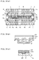
- Figure 3 is a schematic drawing illustrating the second embodiment, with Figure 3(a) presenting a schematic plan view, Figure 3(b) presenting an enlargement of the area A' in Figure 3(a) and Figure 3(c) presenting a cross section through line B'-B' in Figure 3(d) viewed from the direction indicated by the arrows.
- the semiconductor device in the second embodiment has an LOC structure, and is provided with an on-chip semiconductor element 1, a plurality of leads L connected on a substrate 1a of the semiconductor element 1 via an insulating tape T, common lines 2a and 2b for achieving electrical continuity of the electrode pads that handle a common signal among the plurality of electrode pads provided on the substrate 1a and bonding wires W for electrically coupling the electrode pads with the leads L.
- the common line 2a which is electrically continuous with the electrode pads Pa and Pb that receive the source supply
- the common line 2b which is electrically continuous with the electrode pads Pc, Pd, Pe and Pf constituting the ground
- a 3-layer structure a first insulating adhesive tape 21, a copper foil 22a, a second insulating adhesive tape 23
- Figure 3(b) shows a state in which only the copper foil 22a is formed on the first insulating adhesive tape 21 constituting the lowermost layer.
- the copper foil 22a is laminated via the metal bumps BP positioned at the holes.
- the second insulating adhesive tape 23 which, like the first insulating adhesive tape 21, is constituted by applying a thermosetting adhesive on tape, is applied to cover at least the surface of the copper foil 22a.
- the holes are formed in the first insulating adhesive tape 21 constituting the lower layer at positions that coincide with the positions of the electrode pads P1 and the electrode pads Pa and Pb and an electrically continuous line for obtaining the source is constituted with the copper foil 22a via the metal bumps BP positioned at those holes.
- the copper foil 22a is insulated from the bonding wires W.
- the holes are formed in the first insulating adhesive tape 21 constituting the lower layer at positions that coincide with the positions of the electrode pads P2 and the electrode pads Pc, Pd, Pe and Pf, and an electrically continuous ground line is constituted with the copper foil 22a via the metal bumps BP positioned at those holes.
- the copper foil 22a is insulated from the bonding wires W.
- each of the common lines 2a and 2b is approximately 45 ⁇ 50 micrometer (the first insulating adhesive tape 21 and the second insulating adhesive tape 23 are approximately 20 micrometer each in thickness and the copper foil 22a is approximately 5 micrometer in thickness) and by setting their dimensions thus, the loop height of the bonding wires W that lie astride these lines can be reduced compared to that in the prior art. Moreover, because of the second insulating adhesive tape 23 formed on the surface, no short circuit occurs even if the bonding wires W come in contact with the common lines 2a and 2b.
- the first insulating adhesive tape 21 with a thermosetting adhesive applied on its upper surface and lower surface is applied onto the substrate 1a under heat and pressure.
- the first insulating adhesive tape 21 is applied with the holes formed at positions that coincide with the positions of the electrode pads P1, Pa and Pb that handle the source signal
- the first insulating adhesive tape 21 is applied with the holes formed at positions that coincide with the positions of the electrode pads P2, Pc, Pd, Pe and Pf that handle the ground signal.
- a metal bump BP is provided on each of the electrode pads within these holes.
- the copper foil 22a is then adhered onto the first insulating adhesive tape 21 under pressure.
- the second insulating adhesive tape 23, with a thermosetting adhesive applied onto its lower surface, is then adhered onto the copper foil 22a under pressure.
- the width of the copper foil 22a that is adhered should be smaller than the width of the first insulating adhesive tape 21 and the second insulating adhesive tape 23.
- thermosetting adhesive applied to the first insulating adhesive tape 21 and the second insulating adhesive tape 23 sets and contracts so that the copper foil 22a and the metal bumps BP come very firmly into contact with each other.
- the electrode pads that are not connected with the common lines 2a or 2b are electrically coupled with the leads L through the bonding wires W.
- the bonding wires W lie astride the common lines 2a and 2b and are also supported by and in contact with the second insulating adhesive tape 23 on the surfaces of the common lines 2a and 2b. This achieves a lower loop for the bonding wires W and also a sufficient degree of shape retention.
- the entirety of the semiconductor element 1 is sealed into a package with a molding resin (not shown).
- a molding resin not shown.
- the copper foil 22a is used to constitute the electrically continuous area of the common lines 2a and 2b, it becomes possible to achieve an improvement in the electrical characteristics, since the electrically continuous lines will have low resistance.
- FIGS. 4 and 5 are schematic drawings illustrating the third embodiment, with Figure 4(a) presenting a schematic plan view, Figure 4(b) presenting an enlargement of the area C in Figure 4(a), Figure 5(a) showing the shape of the first conductive adhesive, Figure 5(b) presenting a cross section through line D-D in Figure 4(b) viewed from the direction indicated with the arrow and Figure 5(c) presenting a schematic cross section illustrating a packaged state.
- Figure 4(a) illustrates the semiconductor device in the third embodiment, which has an LOC structure and is provided with an on-chip semiconductor element 1, a plurality of leads L connected on a substrate 1a of the semiconductor element 1 via an insulating tape T, common lines 2a and 2b for achieving electrical continuity of the electrode pads that handle a common signal among the plurality of electrode pads provided on the substrate 1a and bonding wires W for electrically coupling the electrode pads with the leads L.
- the third embodiment is characterized in that the line electrically continuous with the electrode pads Pa and Pb, which receives source supply, and the line electrically continuous with the electrode pads Pc, Pd, Pe and Pf constituting the ground, are constituted with a 5-layer structure.
- the 5-layer structure is achieved by sequentially laminating a first insulating adhesive tape 21 constituting the lowermost layer, a first conductive adhesive 22 toward the lower layer, a second insulating adhesive tape 23 constituting an intermediate layer, a second conductive adhesive 24 toward the upper layer and a third insulating adhesive tape 25 constituting the uppermost layer.
- the first insulating adhesive tape 21 which is constituted by applying a thermoplastic adhesive onto tape, is applied with holes formed at positions coinciding with the positions of electrode padsfor source supply (including other electrode pads continuous with these electrode pads in subsequent explanations) and with holes formed at positions coinciding with the positions of the electrode pads for ground (including other electrode pads continuous with these electrode pads in subsequent explanations).
- the first conductive adhesive 22 is applied so that it enters the holes in the first insulating adhesive tape 21 at positions corresponding to the electrode pads for source supply (e.g., electrode pad Pa) while avoiding the positions of other electrode pads P (see Figure 5(a)).
- the second insulating adhesive tape 23 which is constituted by applying a thermoplastic adhesive onto tape, is applied covering the surface of the first conductive adhesive 22. It is to be noted that holes are formed in this second insulating adhesive tape 23 at positions that correspond to the positions of the electrode pads for ground and other electrode pads (electrode pads other than those for source supply or ground).
- the second conductive adhesive 24 is applied so that it enters the holes in the second insulating adhesive tape 23 formed at positions corresponding to the electrode pads for ground (e.g., electrode pad Pa) while avoiding the positions of other electrode pads P (electrode pads other than those for source supply or ground).
- the third insulating adhesive tape 25 which is constituted by applying a thermoplastic adhesive onto tape, is applied covering the surface of the second conductive adhesive 24. Holes are formed in this third insulating adhesive tape 23 at positions that correspond to the positions of the electrode pads other than those for source supply or ground.
- the first conductive adhesive 22 toward the lower layer constitutes a continuous line for source supply whereas the second conductive adhesive 24 toward the upper layer constitutes the continuous line for ground.
- the first conductive adhesive 22 and the second conductive adhesive 24 achieving a laminated structure, each of them passes on both sides of the electrode pads.
- the bonding wires W are connected at these holes to achieve electrical coupling with the leads L.
- the first insulating adhesive tape 21 with holes formed at positions that coincide with the individual electrode pads is adhered under heat and pressure.
- the first conductive adhesive 22 is applied onto the first insulating adhesive tape 21.
- the first conductive adhesive 22 is applied so that it passes over both sides of each electrode pad and enters only into the holes formed over the electrode pads P1, Pa and Pb that handle the source signal (see Figure 5(a)).
- the application of the first conductive adhesive 22 is performed by employing one of the methods illustrated in FIGS. 2(a) ⁇ 2(c), as in the first embodiment.
- the second insulating adhesive tape 23 is adhered onto the first conductive adhesive 22 under heat and pressure. It is to be noted that holes are formed in the second insulating adhesive tape 23 at positions that coincide with the positions of the electrode pads P2, Pc, Pd, Pe and Pf for ground and also with other electrode pads (electrode pads other than those for source supply or ground).
- the second conductive adhesive 24 is applied onto the second insulating adhesive tape 23.
- the second conductive adhesive 24 is applied so that it passes over both sides of each electrode pad and enters only into the holes formed over the electrode pads P2, Pc, Pd, Pe and Pf that handle the ground signal.
- the application of the second conductive adhesive 24 is performed by employing one of the methods illustrated in FIGS. 2(a) ⁇ 2(c), as in the case of the first conductive adhesive 22.
- the third insulating adhesive tape 25 is adhered under heat and pressure onto the second conductive adhesive 24 thus applied.
- the third insulating adhesive tape 25 covers the second conductive adhesive 24. It is to be noted that holes are formed in the third conductive adhesive tape 25 at positions that coincide with the positions of electrode pads other than those for source supply or ground.
- the semiconductor element 1 After forming the 5-layer common lines 2 through lamination, the semiconductor element 1 is heated. Through this heating, the thermoplastic adhesive is set, thereby bonding the individual layers.
- the electrode pads that are not connected to the common lines 2 are electrically coupled with the leads L through the bonding wires W.
- the bonding wires W achieve a state in which they lie astride the common lines 2 and are supported by and in contact with the third insulating adhesive tape 25 on the surfaces of the common lines 2. With this, a lower loop is achieved for the bonding wires W and, at the same time, sufficient shape retention is achieved.
- the entirety of the semiconductor element 1 is sealed with a molding resin, as shown in Figure 5(e), to constitute a package PC. Since the loops of the bonding wires W in this embodiment can be low compared to the prior art, the thickness of the package PC can be reduced to that indicated with the 2-point chain line in the figure.
- the common lines 2 by constituting the common lines 2 as a 5-layer structure, a state is achieved in which independent continuous lines independently pass over both sides of the electrode pads, thereby increasing the overall width (area of adhesion).
- this effect becomes more marked as the pitch of the individual electrode pads becomes smaller.
- the source line for source supply and the ground line for grounding constitute the common lines
- the present invention is not restricted to these examples, and any line for achieving electrical continuity for a plurality of electrode pads that handle a common signal may constitute a common line.
- aluminum wiring or the like inside the semiconductor element 1 may be used as a common line.
- the following advantages are achieved through the semiconductor device and its manufacturing method according to the present invention. Namely, even when the bonding wires are connected astride common lines, it is not necessary to take into consideration the possibility of electrical contact between the common lines and the bonding wires, thereby making it possible to reduce the height of the loops of the bonding wire. Thus, a thinner package is achieved for the semiconductor device.
Landscapes
- Wire Bonding (AREA)
- Lead Frames For Integrated Circuits (AREA)
Applications Claiming Priority (2)
| Application Number | Priority Date | Filing Date | Title |
|---|---|---|---|
| JP76780/97 | 1997-03-28 | ||
| JP07678097A JP3627949B2 (ja) | 1997-03-28 | 1997-03-28 | 半導体装置およびその製造方法 |
Publications (2)
| Publication Number | Publication Date |
|---|---|
| EP0867938A2 true EP0867938A2 (de) | 1998-09-30 |
| EP0867938A3 EP0867938A3 (de) | 1999-03-10 |
Family
ID=13615121
Family Applications (1)
| Application Number | Title | Priority Date | Filing Date |
|---|---|---|---|
| EP97308718A Withdrawn EP0867938A3 (de) | 1997-03-28 | 1997-10-30 | Halbleiteranordnung mit Elektrodenflächen und Leiter |
Country Status (6)
| Country | Link |
|---|---|
| US (1) | US6137166A (de) |
| EP (1) | EP0867938A3 (de) |
| JP (1) | JP3627949B2 (de) |
| KR (1) | KR100366114B1 (de) |
| CN (1) | CN1147931C (de) |
| TW (1) | TW392260B (de) |
Families Citing this family (4)
| Publication number | Priority date | Publication date | Assignee | Title |
|---|---|---|---|---|
| KR100561549B1 (ko) * | 1999-10-07 | 2006-03-17 | 삼성전자주식회사 | 패드 온 칩형 반도체 패키지 |
| DE10025774A1 (de) * | 2000-05-26 | 2001-12-06 | Osram Opto Semiconductors Gmbh | Halbleiterbauelement mit Oberflächenmetallisierung |
| US7626262B2 (en) * | 2006-06-14 | 2009-12-01 | Infineon Technologies Ag | Electrically conductive connection, electronic component and method for their production |
| TW201205098A (en) * | 2010-07-16 | 2012-02-01 | Chroma Ate Inc | Inspection fixture for semiconductor die test maintaining flatness of carrier portion |
Citations (4)
| Publication number | Priority date | Publication date | Assignee | Title |
|---|---|---|---|---|
| US4034399A (en) * | 1976-02-27 | 1977-07-05 | Rca Corporation | Interconnection means for an array of majority carrier microwave devices |
| US5252854A (en) | 1990-05-20 | 1993-10-12 | Hitachi, Ltd. | Semiconductor device having stacked lead structure |
| US5319241A (en) | 1991-01-23 | 1994-06-07 | Texas Instruments Incorporated | Lead frame without power buses for lead on chip package, and a semiconductor device with conductive tape power distribution |
| JPH06286659A (ja) | 1993-03-31 | 1994-10-11 | Suzuki Motor Corp | ペダルブラケットの構造 |
Family Cites Families (2)
| Publication number | Priority date | Publication date | Assignee | Title |
|---|---|---|---|---|
| JPH05114622A (ja) * | 1991-10-23 | 1993-05-07 | Hitachi Ltd | 半導体装置 |
| JPH06283659A (ja) * | 1993-03-25 | 1994-10-07 | Mitsubishi Electric Corp | 半導体装置 |
-
1997
- 1997-03-28 JP JP07678097A patent/JP3627949B2/ja not_active Expired - Fee Related
- 1997-10-18 TW TW086115366A patent/TW392260B/zh not_active IP Right Cessation
- 1997-10-30 EP EP97308718A patent/EP0867938A3/de not_active Withdrawn
- 1997-11-28 CN CNB971141134A patent/CN1147931C/zh not_active Expired - Fee Related
- 1997-12-03 US US08/984,049 patent/US6137166A/en not_active Expired - Fee Related
- 1997-12-12 KR KR1019970068290A patent/KR100366114B1/ko not_active Expired - Fee Related
Patent Citations (4)
| Publication number | Priority date | Publication date | Assignee | Title |
|---|---|---|---|---|
| US4034399A (en) * | 1976-02-27 | 1977-07-05 | Rca Corporation | Interconnection means for an array of majority carrier microwave devices |
| US5252854A (en) | 1990-05-20 | 1993-10-12 | Hitachi, Ltd. | Semiconductor device having stacked lead structure |
| US5319241A (en) | 1991-01-23 | 1994-06-07 | Texas Instruments Incorporated | Lead frame without power buses for lead on chip package, and a semiconductor device with conductive tape power distribution |
| JPH06286659A (ja) | 1993-03-31 | 1994-10-11 | Suzuki Motor Corp | ペダルブラケットの構造 |
Also Published As
| Publication number | Publication date |
|---|---|
| KR100366114B1 (ko) | 2003-02-19 |
| JP3627949B2 (ja) | 2005-03-09 |
| US6137166A (en) | 2000-10-24 |
| KR19980079528A (ko) | 1998-11-25 |
| CN1195191A (zh) | 1998-10-07 |
| EP0867938A3 (de) | 1999-03-10 |
| CN1147931C (zh) | 2004-04-28 |
| JPH10270491A (ja) | 1998-10-09 |
| TW392260B (en) | 2000-06-01 |
Similar Documents
| Publication | Publication Date | Title |
|---|---|---|
| CN100561737C (zh) | 中心焊点芯片的叠层球栅极阵列封装件及其制造方法 | |
| US6642610B2 (en) | Wire bonding method and semiconductor package manufactured using the same | |
| US6208021B1 (en) | Semiconductor device, manufacturing method thereof and aggregate type semiconductor device | |
| US6087717A (en) | Semiconductor device and manufacturing method | |
| US7723839B2 (en) | Semiconductor device, stacked semiconductor device, and manufacturing method for semiconductor device | |
| KR100368698B1 (ko) | 반도체패키지와,그것을이용한반도체장치및그제조방법 | |
| US5874784A (en) | Semiconductor device having external connection terminals provided on an interconnection plate and fabrication process therefor | |
| US5612259A (en) | Method for manufacturing a semiconductor device wherein a semiconductor chip is mounted on a lead frame | |
| TWI520240B (zh) | 功率型晶片上引線之球柵陣列封裝 | |
| US20010034082A1 (en) | Semiconductor package and semiconductor package fabrication method | |
| JPH11204720A (ja) | 半導体装置及びその製造方法 | |
| US20020109216A1 (en) | Integrated electronic device and integration method | |
| JPH10242210A (ja) | 集積回路装置の実装構造およびその製造方法 | |
| WO1996013855A1 (en) | A leadframe for an integrated circuit package which electrically interconnects multiple integrated circuit die | |
| JP2000101016A (ja) | 半導体集積回路装置 | |
| US5780923A (en) | Modified bus bar with Kapton™ tape or insulative material on LOC packaged part | |
| US6897088B2 (en) | Method for connecting circuit devices | |
| US6137166A (en) | Semiconductor device | |
| US6580157B2 (en) | Assembly and method for modified bus bar with Kapton™ tape or insulative material in LOC packaged part | |
| JPH10303249A (ja) | 半導体装置 | |
| TW200933868A (en) | Stacked chip package structure | |
| KR100947146B1 (ko) | 반도체 패키지 | |
| JP2747260B2 (ja) | セラミック複合リードフレーム及びそれを用いた半導体 装置 | |
| JPH05326621A (ja) | Tabフィルム及びそのtabフィルムを用いた半導体装置 | |
| JP2862081B2 (ja) | Icチップの実装構造 |
Legal Events
| Date | Code | Title | Description |
|---|---|---|---|
| PUAI | Public reference made under article 153(3) epc to a published international application that has entered the european phase |
Free format text: ORIGINAL CODE: 0009012 |
|
| AK | Designated contracting states |
Kind code of ref document: A2 Designated state(s): DE FR GB IT NL |
|
| AX | Request for extension of the european patent |
Free format text: AL;LT;LV;RO;SI |
|
| PUAL | Search report despatched |
Free format text: ORIGINAL CODE: 0009013 |
|
| AK | Designated contracting states |
Kind code of ref document: A3 Designated state(s): AT BE CH DE DK ES FI FR GB GR IE IT LI LU MC NL PT SE |
|
| AX | Request for extension of the european patent |
Free format text: AL;LT;LV;RO;SI |
|
| 17P | Request for examination filed |
Effective date: 19990830 |
|
| AKX | Designation fees paid |
Free format text: AT BE CH DE DK LI |
|
| RBV | Designated contracting states (corrected) |
Designated state(s): DE FR GB IT NL |
|
| 17Q | First examination report despatched |
Effective date: 20031113 |
|
| STAA | Information on the status of an ep patent application or granted ep patent |
Free format text: STATUS: THE APPLICATION IS DEEMED TO BE WITHDRAWN |
|
| 18D | Application deemed to be withdrawn |
Effective date: 20140501 |