EP0867984A2 - Fabrication de circuits intégrés photoniques - Google Patents
Fabrication de circuits intégrés photoniques Download PDFInfo
- Publication number
- EP0867984A2 EP0867984A2 EP98301969A EP98301969A EP0867984A2 EP 0867984 A2 EP0867984 A2 EP 0867984A2 EP 98301969 A EP98301969 A EP 98301969A EP 98301969 A EP98301969 A EP 98301969A EP 0867984 A2 EP0867984 A2 EP 0867984A2
- Authority
- EP
- European Patent Office
- Prior art keywords
- layer
- waveguide
- active
- active region
- passive
- Prior art date
- Legal status (The legal status is an assumption and is not a legal conclusion. Google has not performed a legal analysis and makes no representation as to the accuracy of the status listed.)
- Withdrawn
Links
Images


Classifications
-
- H—ELECTRICITY
- H01—ELECTRIC ELEMENTS
- H01S—DEVICES USING THE PROCESS OF LIGHT AMPLIFICATION BY STIMULATED EMISSION OF RADIATION [LASER] TO AMPLIFY OR GENERATE LIGHT; DEVICES USING STIMULATED EMISSION OF ELECTROMAGNETIC RADIATION IN WAVE RANGES OTHER THAN OPTICAL
- H01S5/00—Semiconductor lasers
- H01S5/02—Structural details or components not essential to laser action
- H01S5/026—Monolithically integrated components, e.g. waveguides, monitoring photo-detectors, drivers
-
- G—PHYSICS
- G02—OPTICS
- G02B—OPTICAL ELEMENTS, SYSTEMS OR APPARATUS
- G02B6/00—Light guides; Structural details of arrangements comprising light guides and other optical elements, e.g. couplings
- G02B6/10—Light guides; Structural details of arrangements comprising light guides and other optical elements, e.g. couplings of the optical waveguide type
- G02B6/12—Light guides; Structural details of arrangements comprising light guides and other optical elements, e.g. couplings of the optical waveguide type of the integrated circuit kind
- G02B6/12004—Combinations of two or more optical elements
-
- G—PHYSICS
- G02—OPTICS
- G02B—OPTICAL ELEMENTS, SYSTEMS OR APPARATUS
- G02B6/00—Light guides; Structural details of arrangements comprising light guides and other optical elements, e.g. couplings
- G02B6/10—Light guides; Structural details of arrangements comprising light guides and other optical elements, e.g. couplings of the optical waveguide type
- G02B6/12—Light guides; Structural details of arrangements comprising light guides and other optical elements, e.g. couplings of the optical waveguide type of the integrated circuit kind
- G02B2006/12083—Constructional arrangements
- G02B2006/12128—Multiple Quantum Well [MQW]
-
- G—PHYSICS
- G02—OPTICS
- G02B—OPTICAL ELEMENTS, SYSTEMS OR APPARATUS
- G02B6/00—Light guides; Structural details of arrangements comprising light guides and other optical elements, e.g. couplings
- G02B6/10—Light guides; Structural details of arrangements comprising light guides and other optical elements, e.g. couplings of the optical waveguide type
- G02B6/12—Light guides; Structural details of arrangements comprising light guides and other optical elements, e.g. couplings of the optical waveguide type of the integrated circuit kind
- G02B2006/12166—Manufacturing methods
- G02B2006/12176—Etching
-
- G—PHYSICS
- G02—OPTICS
- G02B—OPTICAL ELEMENTS, SYSTEMS OR APPARATUS
- G02B6/00—Light guides; Structural details of arrangements comprising light guides and other optical elements, e.g. couplings
- G02B6/10—Light guides; Structural details of arrangements comprising light guides and other optical elements, e.g. couplings of the optical waveguide type
- G02B6/12—Light guides; Structural details of arrangements comprising light guides and other optical elements, e.g. couplings of the optical waveguide type of the integrated circuit kind
- G02B2006/12166—Manufacturing methods
- G02B2006/12178—Epitaxial growth
Definitions
- This invention relates to photonic integrated circuit devices with both passive and active optical waveguide structures.
- PICs photonic integrated circuits
- buried rib guides are preferred in non-thresholding devices such as couplers, switches, and filters.
- a problem in the aforementioned optoelectronic-electronic category is the requirement for current blocking in lasers.
- the typical laser device in PIC technology has a mesa structure.
- An example of this type of laser structure is a semi-insulating planar buried heterostructure ( SIPBH ) type laser as described by B. I. Miller, U. Koren, and R. J. Capik, Electron. Lett. 22,947 (1986).
- SIPBH semi-insulating planar buried heterostructure
- the two planarity objectives described above can be relatively easily realized separately, but to date achieving both in a reliable, and cost effective process, and one that yields a truly integrated planar structure, has been elusive. Since the requirement for a planar optical interface cannot be compromised, the current processing sequence used to form the mesa (laser) structure and the buried rib waveguide of current PIC devices results in a severely stepped surface. A PIC device design, and a processing sequence, that produce a planar device surface, without compromising the device requirements outlined above, would be a major advance in PIC technology.
- a new general PIC device has been developed, and a process sequence for making that device, that produces a laser waveguide structure that is essentially coplanar with an associated passive buried rib waveguide, and produces also a surface topography that is essentially planar.
- the severe mesa for the laser device is eliminated, without additional process complexity, and without diminishing device performance.
- the PIC design of the invention is particularly suited for laser or amplifier arrays.
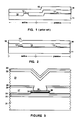
- FIG. 1 the surface non-planarity of prior art PIC devices is illustrated. As is known in the art these devices typically have a complex layered structure.
- the cross section of Fig. 1 is simplified to show just the essential active and passive elements side by side.
- An n-type InP substrate is shown at 11 with one side a passive waveguide section and the other an active device section.
- the waveguide layer 12 and the mesa structure on the active portion is a semi-insulating blocked buried heterostructure multi-quantum well laser waveguide.
- On the passive portion is a buried rib semiinsulating-clad waveguide 13.
- a semi-insulating layer 14 is deposited which fills the deep etched regions on the active side and serves as a lateral blocking layer for the laser waveguide 12.
- layer 14 forms a low-loss upper cladding for the passive waveguide.
- layer 14 also produces a substantial step 15.
- the p-type InP upper cladding layer 16 for the laser waveguide 12 is deposited over layer 14 and replicates step 15, leaving a non-planar surface. Details of this device technology are given in "Semiconductor Photonic Integrated Circuits", Thomas L. Koch and Uziel Koren, IEEE Journal of Quantum Electronics, Vol. 27, No. 3, March 1991, pp. 641-653, and U.S. Patent No. 5,288,659 issued February 22, 1994 to Thomas L. Koch and Uziel Koren, both of which, to the extent necessary for a complete description, are incorporated herein by reference.
- the PIC structure according to the invention is illustrated in a schematic view similar to that of Fig.1 with the corresponding elements being denoted by the same reference numbers. It is evident that in the structure of the invention the step 15 that appears in the prior art structure has been eliminated.
- the layer 14 in Fig. 2 is essentially planar, as is the upper cladding layer 16 except for a localized depression 17.
- the transition between the active and passive regions, as well as the major portion of the device surface, preferably has no steps greater than approximately 2000 Angstroms.
- Fig. 3 represents a passive portion of the PIC
- Fig. 4 an active portion.
- Common reference numerals are used where the same feature is presented in both sections. It will be understood by those skilled in the art that the various elements in Figs. 3 and 4 are not necessarily drawn to scale. Many of the details given herein to enable one skilled in the art to practice the invention are given by way of example, and represent a variety of options that are within the skill and choice of the device and process designers.
- the substrate shown at 21 is an n-type InP relatively heavily doped semiconductor substrate.
- the primary waveguide stack is formed on substrate 21 in the first of three epitaxial growth operations.
- the primary waveguide stack includes four layers 22-25. These layers can be grown by Metal-Organic Chemical Vapor Deposition ( MOCVD ) or Molecular Beam Epitaxy ( MBE ) using procedures well known in the art.
- MOCVD Metal-Organic Chemical Vapor Deposition
- MBE Molecular Beam Epitaxy
- a second passive waveguide layer 23 of InGaAsP with a ⁇ PL 1.3 and a thickness comparable to the thickness of layer 22 is grown over that layer.
- the third layer 24 is a MQW layer which is the active layer of the lasers.
- the fourth layer 25 is a relatively thin, i.e. 500-1000 Angstroms, protective layer of p-type InP. This protective layer serves to insure that the region above the active quantum well layer remains p-type to prevent remote or parasitic junction formation away from the quantum well junctions and impair their current injection efficiency.
- the active MQW layer is desirably thin, i.e. less than 2500 Angstroms, to minimize the step between the quantum wells and the associated waveguide layers 22-23.
- the active and passive regions of the PIC are defined by a chemically selective etch using a standard SiO 2 or photoresist mask as will be described in more detail below.
- a second epitaxial growth operation is performed to create the blocking regions of the PIC.
- the blocking layer in this embodiment is relatively thick, i.e. 1-3 ⁇ m, and comprises, in the particular embodiment described here, a stop etch quaternary layer 26 of 1.1 ⁇ PL , approximately 200-300 Angstroms in thickness, a thick, 1.2 - 1.4 ⁇ m, undoped InP layer 27, a p-InP layer 28, and an n-type InP layer 29.
- the undoped layer serves the primary blocking function.
- This layer may alternatively be made more insulating by iron doping.
- the n-type and p-type layers form a reverse biased junction that further inhibits current flow through the blocking layer.
- the thickness of these layers is that required to support a p-n junction, i.e. a few hundred to a few thousand Angstroms.
- the contact vias for the active elements are defined by selectively removing the blocking layer over the active regions.
- the top p-InP layer 31 is then grown in the third growth operation which fills the recesses over the active regions, leaving a slight V-shaped surface depression as shown. This layer is relatively thick, i.e. 1.5 - 3.0 ⁇ m, to fill the slot over the active regions.
- the contact layer 32 is a ternary layer of InGaAs with a thickness of the order of 2000 - 4000 Angstroms.
- Metallized Au-Zn contact pad 33 which is representative of a planar metallization pattern, completes the structure.
- the surface of the PIC is planar and additional metallization patterns, and contact pads, can be applied with nearly total design freedom.
- Fig. 4 shows a passive section of the PIC and illustrates the coplanarity between the active and passive waveguides as well as the essentially coplanarity of the corresponding layers in both the active and passive sections up to and including the surface layers.
- the reference numbers show layers common to both structures.
- the passive waveguide is shown at 34.
- the InP substrate 51 is shown with layers of the primary waveguide stack deposited on the substrate.
- Layer 52 is InGaAsP with a photoluminescent wavelength, ⁇ PL , of 1.1 and a thickness of 1000 to 5000 Angstroms.
- the active multiquantum well (MQW) layer is shown at 54 and comprises a series of typically 3-10 quantum wells each with a thickness of the order of 30-100 Angstroms. The wells are typically separated by 100-200 Angstroms of higher bandgap barriers. In the structure shown, the active layer has a thickness of approximately 1000 Angstroms.
- the material of the active layer depends on the emitting wavelength desired.
- the MQW material may be Ga 0.8 In 0.2 As and the barrier layers GaAs.
- the quantum wells are typically quaternary InGaAsP compositions with boundary layers of higher bandgap quaternary material. In this description, no attempt is made to include the many possible permutations, e.g. single quantum wells, superlattices, graded bandgap regions, that can be used with this kind of laser diode structure.
- the typical PIC may have several or many active regions and various different forms of active devices such as modulators and amplifiers.
- the materials suitable for these devices and waveguides are typically these materials. Typically these materials are combinations of Al, Ga, and In with As and P. These combinations are sufficiently established in this technology that layers such as layers 51-55 are characterized by optical properties, e.g. ⁇ PL and those skilled in the art know the compositions and processing required to produce the layers.
- the final layer of the primary stack is a protective layer 55 of p-type InP, approximately 200-3000 Angstroms and preferably 400-800 Angstroms, to prevent remote junction formation in the vicinity of the quantum well layer as mentioned earlier.
- Layers 52-55 are grown by Metal-Organic Chemical Vapor Deposition
- MOCVD Metal Organic Chemical Vapor Deposition
- MBE Molecular Beam Epitaxy
- a bulk layer can be used for bulk lasers or for modulators or amplifiers.
- a bulk layer is a 300-2000 Angstrom thick quaternary layer.
- the term active layer or region is intended to include such bulk layer structures.
- the main feature of an active layer or region is that it is electrically accessible to activate it.
- the primary waveguide stack is then patterned to form the active regions and their associated waveguides, and the passive waveguide regions.
- the passive waveguide sections are shown in Figs. 5 and 8-14 alongside the active sections.
- the passive sections typically interconnect, in a longitudinal dimension (with respect to the direction of light propagation), active regions of the PIC.
- plan views of the PIC are helpful.
- Figs. 6 and 7 are plan views of a section of a typical PIC , 81, with the width dimension along the x-axis and the longitudinal dimension along the y-axis.
- FIG. 6 shows the first step in defining the active region, i.e. the removal of unwanted portions of the protective layer 55 and the active MQW layer 54.
- An active portion of the circuit is shown at 81 in Fig. 6 covered with layer 55.
- Etch mask 56 is shown covering the active regions to be retained. In this etch step only the longitudinal (y-axis) boundaries of the active regions are defined.
- a schematic side section is shown connected to the plan view by dashed lines 82. The side view shows the position of the etch mask 56 with respect to the substrate and is included to illustrate the etching strategy for the process. The multiple layers have been omitted for simplicity. Layers 55 and 54 are then etched away using mask 56 to define the etch boundary, leaving a stripe of active material across the width (x-axis) of the device section.
- etch procedures known in the art can be used to etch the various layers described in this work. Dry etch or plasma etches are frequently used in this technology. To make the embodiments described here wet etches were used, both selective etches and non-selective etches.
- the non-selective etchant was 1:1:10 H 2 O 2 , HBr , H 2 O.
- the InP selective etch was 2:1 HCl, H 3 PO 4
- the quaternary selective etch was 1:1:3 H 2 O 2 , H 2 O, H 2 SO 4 .
- Fig. 7 shows a plan view of the same PIC section shown in Fig. 6 with etch mask 58 overlying the waveguide boundaries for all waveguides in the circuit.
- a front view of the masked substrate 81 is shown connected to the plan view by dashed lines 82 for further clarity. Again, the figure is presented to describe the etching strategy and the details, e.g. the multiple layers, are not shown.
- the top layer in the unmasked portion of Fig. 7 is layer 53, layers 55 and 54 having been removed from these regions in the etch step described in connection with Fig. 6.
- mask 58 covers both active regions and passive waveguides.
- the active regions in Fig. 7 are indicated by the area 83.
- etch strategy illustrated in Figs. 6 and 7 is shown implemented in the device cross section in Figs. 8 and 9, with Fig. 8 showing the multilayer structure after the etch described in connection with Figure 6, and Fig. 9 corresponding to Fig. 7 but showing the active and passive regions separately with the etch mask 58 in place.
- the PIC sections appear as in Fig.10.
- the etch is stopped after partially removing waveguide layer 53 as shown.
- the resulting layer has a waveguide portion 59 which is substantially thicker, i.e. 300-1000 Angstroms, than the thickness of layers 52,53.
- a corresponding thick region of layers 52,53 is formed under the active region.
- the thick portion of the layer serves as the guiding region.
- the width of the waveguide stripes is typically in the range 1.5-3.0 microns.
- the objective is to maintain a single mode guide in the passive regions of the PIC.
- Thin waveguide layers are single mode to relatively large widths, while thicker waveguide regions should be narrower to retain single mode guide characteristics.
- a supplemental etch step is recommended to fully isolate the active regions.
- the preferred situation is to have the etch step that defines the waveguide width also etch through the unmasked thickness of the active region. That condition suggests that the thickness of the active layer be less than the depth of the etch used to define the waveguides, i.e. the difference between the thickness of region 59 and the thickness of layer 53.
- the blocking layer in the particular embodiment described here, comprises a first etch stop layer 68, which is a 1.1 ⁇ PL quaternary InGaAsP layer approximately 200-300 Angstroms thick.
- the primary blocking layer 601 is undoped InP and has a thickness of 1.2-1.4 ⁇ m.
- a pnp structure is created by p-type InP layer 62 and n-type InP layer 63, both approximately 2000 Angstroms in thickness. These four layers are also preferably grown in a single uninterrupted growth operation.
- a photomask 64 is applied over the multiple blocking layers to define an opening 65 for the active region electrical via.
- An InP selective etch is used which stops at the etch stop layer 68.
- the third growth operation is performed to produce a thick p-type cladding layer 66 as shown in Fig. 13. This layer may be 1-3 ⁇ m thick and fills the slot 65 (Fig. 12) leaving a slight depression 67 in the surface of the device.
- the capping layer 71 shown in Fig. 14, is grown at this stage and consists of approximately 3000 Angstroms of InGaAs.
- the contact layer 72 is an alloyed layer of Au-Zn which may be sputtered or evaporated and alloyed using conventional techniques. This layer is representative of an ohmic contact pad.
- An additional runner in a metallization pattern may also be used, and may have a composition selected from a variety of materials, e.g. TiPtAu. This second metallization pattern is commonly used for bonding pads.
- PIC devices are typically coupled to input/output assemblies which may include one or more optical fibers.
- the planar configuration described here is particularly suited for arrays of optical amplifiers, switches and/or modulators, and these device arrays generally include many optical fiber input/outputs.
Landscapes
- Physics & Mathematics (AREA)
- General Physics & Mathematics (AREA)
- Optics & Photonics (AREA)
- Condensed Matter Physics & Semiconductors (AREA)
- Electromagnetism (AREA)
- Engineering & Computer Science (AREA)
- Microelectronics & Electronic Packaging (AREA)
- Optical Integrated Circuits (AREA)
- Semiconductor Lasers (AREA)
- Recrystallisation Techniques (AREA)
Applications Claiming Priority (2)
| Application Number | Priority Date | Filing Date | Title |
|---|---|---|---|
| US827598 | 1997-03-28 | ||
| US08/827,598 US5863809A (en) | 1997-03-28 | 1997-03-28 | Manufacture of planar photonic integrated circuits |
Publications (2)
| Publication Number | Publication Date |
|---|---|
| EP0867984A2 true EP0867984A2 (fr) | 1998-09-30 |
| EP0867984A3 EP0867984A3 (fr) | 2004-01-14 |
Family
ID=25249636
Family Applications (1)
| Application Number | Title | Priority Date | Filing Date |
|---|---|---|---|
| EP98301969A Withdrawn EP0867984A3 (fr) | 1997-03-28 | 1998-03-17 | Fabrication de circuits intégrés photoniques |
Country Status (3)
| Country | Link |
|---|---|
| US (1) | US5863809A (fr) |
| EP (1) | EP0867984A3 (fr) |
| JP (1) | JP3306802B2 (fr) |
Families Citing this family (12)
| Publication number | Priority date | Publication date | Assignee | Title |
|---|---|---|---|---|
| JP4117854B2 (ja) * | 1997-06-20 | 2008-07-16 | シャープ株式会社 | 導波路型光集積回路素子及びその製造方法 |
| FR2781577B1 (fr) * | 1998-07-06 | 2000-09-08 | Alsthom Cge Alcatel | Procede de fabrication d'un circuit optique integre |
| US6288821B1 (en) | 1999-10-01 | 2001-09-11 | Lucent Technologies, Inc. | Hybrid electro-optic device with combined mirror arrays |
| JP2001274528A (ja) | 2000-01-21 | 2001-10-05 | Fujitsu Ltd | 薄膜デバイスの基板間転写方法 |
| US7072557B2 (en) * | 2001-12-21 | 2006-07-04 | Infinera Corporation | InP-based photonic integrated circuits with Al-containing waveguide cores and InP-based array waveguide gratings (AWGs) and avalanche photodiodes (APDs) and other optical components containing an InAlGaAs waveguide core |
| KR100427581B1 (ko) | 2002-02-21 | 2004-04-28 | 한국전자통신연구원 | 반도체 광소자의 제조방법 |
| US6771869B2 (en) * | 2002-04-18 | 2004-08-03 | Triquint Technology Holding Co. | Optoelectronic device having a barrier layer associated therewith and a method of manufacture thereof |
| US7412121B2 (en) * | 2002-10-24 | 2008-08-12 | Applied Research And Photonics, Inc. | Nanophotonic integrated circuit and fabrication thereof |
| US9239424B2 (en) * | 2014-01-28 | 2016-01-19 | International Business Machines Corporation | Semiconductor device and method for fabricating the same |
| KR102349774B1 (ko) | 2015-03-11 | 2022-01-10 | 삼성전자주식회사 | 광전 회로 |
| KR20190033282A (ko) * | 2017-09-21 | 2019-03-29 | 삼성전자주식회사 | 증폭 도파 장치 및 이를 포함한 빔 스티어링 장치 |
| GB2636078B (en) * | 2023-11-23 | 2026-04-08 | Ligentec Sa | Photonic Integrated Circuit |
Family Cites Families (6)
| Publication number | Priority date | Publication date | Assignee | Title |
|---|---|---|---|---|
| US4884119A (en) * | 1988-04-22 | 1989-11-28 | American Telephone & Telegraph Company | Integrated multiple quantum well photonic and electronic devices |
| US5147825A (en) * | 1988-08-26 | 1992-09-15 | Bell Telephone Laboratories, Inc. | Photonic-integrated-circuit fabrication process |
| JP2746326B2 (ja) * | 1989-01-10 | 1998-05-06 | 株式会社日立製作所 | 半導体光素子 |
| US5134671A (en) * | 1990-08-03 | 1992-07-28 | At&T Bell Laboratories | Monolithic integrated optical amplifier and photodetector |
| DE4235920C1 (de) * | 1992-10-23 | 1993-11-25 | Siemens Ag | Monolithisch integrierte Laserdiode-Koppler-Kombination |
| JPH0750445A (ja) * | 1993-06-02 | 1995-02-21 | Rohm Co Ltd | 半導体レーザの製法 |
-
1997
- 1997-03-28 US US08/827,598 patent/US5863809A/en not_active Expired - Lifetime
-
1998
- 1998-03-17 EP EP98301969A patent/EP0867984A3/fr not_active Withdrawn
- 1998-03-26 JP JP07988598A patent/JP3306802B2/ja not_active Expired - Lifetime
Also Published As
| Publication number | Publication date |
|---|---|
| JPH10284807A (ja) | 1998-10-23 |
| US5863809A (en) | 1999-01-26 |
| JP3306802B2 (ja) | 2002-07-24 |
| EP0867984A3 (fr) | 2004-01-14 |
Similar Documents
| Publication | Publication Date | Title |
|---|---|---|
| US7941024B2 (en) | Buried heterostructure device having integrated waveguide grating fabricated by single step MOCVD | |
| US6162655A (en) | Method of fabricating an expanded beam optical waveguide device | |
| EP0469681B1 (fr) | Amplificateur optique | |
| US7072557B2 (en) | InP-based photonic integrated circuits with Al-containing waveguide cores and InP-based array waveguide gratings (AWGs) and avalanche photodiodes (APDs) and other optical components containing an InAlGaAs waveguide core | |
| JPH08107251A (ja) | 反射ディジタル同調レーザの作製方法 | |
| US11670908B2 (en) | Planar laser structure with vertical signal transition | |
| US5863809A (en) | Manufacture of planar photonic integrated circuits | |
| US7454111B2 (en) | Optical device of waveguide type and its production method | |
| US6025207A (en) | Method for manufacture of a buried structure laser device for integrated photonic circuit | |
| US5763287A (en) | Method of fabricating semiconductor optical device | |
| JP7248152B2 (ja) | 半導体装置および半導体装置の製造方法 | |
| WO2007107782A1 (fr) | Composants opto-électroniques intégrés monolithiquement | |
| EP0394167B1 (fr) | Formation des faces réfléchissantes d'un laser et intégration des composants optoélectroniques | |
| US6692980B2 (en) | Method for fabricating monolithic integrated semiconductor photonic device | |
| US6309904B1 (en) | Method of fabricating an optical integrated circuit | |
| EP1225670B1 (fr) | Dispositif semi-conducteur avec structure à confinement de courant | |
| EP1719003B1 (fr) | Dispositif a structure enterree fabrique en une seul etape de deposition chimique metal-oxyde en phase vapeur | |
| US5309465A (en) | Ridge waveguide semiconductor laser with thin active region | |
| EP0700082A2 (fr) | Circuits intégrés monolytiques comprenant des dispositifs optiques contrÔlés électriquement étant isolés diélectriquement, et procédé de fabrication de ces circuits | |
| JPH09237940A (ja) | 半導体装置,及びその製造方法 | |
| JP2008166371A (ja) | 光半導体素子及びその製造方法 | |
| Sabnis et al. | Intimate monolithic integration of chip-scale photonic circuits | |
| JP2005286198A (ja) | 光集積素子 | |
| US7279109B2 (en) | Method for manufacturing a photonic device and a photonic device | |
| EP4572039A1 (fr) | Convertisseur de taille de point à indice élevé semi-inulant pour le couplage optique de circuits iii-v sur des circuits hétéro-intégrés en silicium |
Legal Events
| Date | Code | Title | Description |
|---|---|---|---|
| PUAI | Public reference made under article 153(3) epc to a published international application that has entered the european phase |
Free format text: ORIGINAL CODE: 0009012 |
|
| AK | Designated contracting states |
Kind code of ref document: A2 Designated state(s): AT BE CH DE DK ES FI FR GB GR IE IT LI LU MC NL PT SE |
|
| AX | Request for extension of the european patent |
Free format text: AL;LT;LV;MK;RO;SI |
|
| PUAL | Search report despatched |
Free format text: ORIGINAL CODE: 0009013 |
|
| AK | Designated contracting states |
Kind code of ref document: A3 Designated state(s): AT BE CH DE DK ES FI FR GB GR IE IT LI LU MC NL PT SE |
|
| AX | Request for extension of the european patent |
Extension state: AL LT LV MK RO SI |
|
| RIC1 | Information provided on ipc code assigned before grant |
Ipc: 7H 01S 5/026 B Ipc: 7G 02B 6/12 B Ipc: 7H 01S 3/025 A |
|
| AKX | Designation fees paid | ||
| REG | Reference to a national code |
Ref country code: DE Ref legal event code: 8566 |
|
| STAA | Information on the status of an ep patent application or granted ep patent |
Free format text: STATUS: THE APPLICATION IS DEEMED TO BE WITHDRAWN |
|
| 18D | Application deemed to be withdrawn |
Effective date: 20040715 |