EP0871220A2 - Pinbelegung eines Halbleitergehäuses - Google Patents
Pinbelegung eines Halbleitergehäuses Download PDFInfo
- Publication number
- EP0871220A2 EP0871220A2 EP98302724A EP98302724A EP0871220A2 EP 0871220 A2 EP0871220 A2 EP 0871220A2 EP 98302724 A EP98302724 A EP 98302724A EP 98302724 A EP98302724 A EP 98302724A EP 0871220 A2 EP0871220 A2 EP 0871220A2
- Authority
- EP
- European Patent Office
- Prior art keywords
- substrate
- indentations
- electrical circuit
- terminal
- holes
- Prior art date
- Legal status (The legal status is an assumption and is not a legal conclusion. Google has not performed a legal analysis and makes no representation as to the accuracy of the status listed.)
- Withdrawn
Links
Images

Classifications
-
- H—ELECTRICITY
- H10—SEMICONDUCTOR DEVICES; ELECTRIC SOLID-STATE DEVICES NOT OTHERWISE PROVIDED FOR
- H10W—GENERIC PACKAGES, INTERCONNECTIONS, CONNECTORS OR OTHER CONSTRUCTIONAL DETAILS OF DEVICES COVERED BY CLASS H10
- H10W70/00—Package substrates; Interposers; Redistribution layers [RDL]
- H10W70/60—Insulating or insulated package substrates; Interposers; Redistribution layers
- H10W70/62—Insulating or insulated package substrates; Interposers; Redistribution layers characterised by their interconnections
- H10W70/65—Shapes or dispositions of interconnections
- H10W70/657—Shapes or dispositions of interconnections on sidewalls or bottom surfaces of the package substrates, interposers or redistribution layers
-
- H—ELECTRICITY
- H10—SEMICONDUCTOR DEVICES; ELECTRIC SOLID-STATE DEVICES NOT OTHERWISE PROVIDED FOR
- H10W—GENERIC PACKAGES, INTERCONNECTIONS, CONNECTORS OR OTHER CONSTRUCTIONAL DETAILS OF DEVICES COVERED BY CLASS H10
- H10W72/00—Interconnections or connectors in packages
-
- H—ELECTRICITY
- H05—ELECTRIC TECHNIQUES NOT OTHERWISE PROVIDED FOR
- H05K—PRINTED CIRCUITS; CASINGS OR CONSTRUCTIONAL DETAILS OF ELECTRIC APPARATUS; MANUFACTURE OF ASSEMBLAGES OF ELECTRICAL COMPONENTS
- H05K1/00—Printed circuits
- H05K1/02—Details
- H05K1/0213—Electrical arrangements not otherwise provided for
- H05K1/0216—Reduction of cross-talk, noise or electromagnetic interference
- H05K1/0218—Reduction of cross-talk, noise or electromagnetic interference by printed shielding conductors, ground planes or power plane
-
- H—ELECTRICITY
- H05—ELECTRIC TECHNIQUES NOT OTHERWISE PROVIDED FOR
- H05K—PRINTED CIRCUITS; CASINGS OR CONSTRUCTIONAL DETAILS OF ELECTRIC APPARATUS; MANUFACTURE OF ASSEMBLAGES OF ELECTRICAL COMPONENTS
- H05K3/00—Apparatus or processes for manufacturing printed circuits
- H05K3/40—Forming printed elements for providing electric connections to or between printed circuits
- H05K3/403—Edge contacts; Windows or holes in the substrate having plural connections on the walls thereof
-
- Y—GENERAL TAGGING OF NEW TECHNOLOGICAL DEVELOPMENTS; GENERAL TAGGING OF CROSS-SECTIONAL TECHNOLOGIES SPANNING OVER SEVERAL SECTIONS OF THE IPC; TECHNICAL SUBJECTS COVERED BY FORMER USPC CROSS-REFERENCE ART COLLECTIONS [XRACs] AND DIGESTS
- Y10—TECHNICAL SUBJECTS COVERED BY FORMER USPC
- Y10T—TECHNICAL SUBJECTS COVERED BY FORMER US CLASSIFICATION
- Y10T29/00—Metal working
- Y10T29/49—Method of mechanical manufacture
- Y10T29/49002—Electrical device making
- Y10T29/49117—Conductor or circuit manufacturing
- Y10T29/49124—On flat or curved insulated base, e.g., printed circuit, etc.
- Y10T29/49155—Manufacturing circuit on or in base
- Y10T29/49165—Manufacturing circuit on or in base by forming conductive walled aperture in base
Definitions
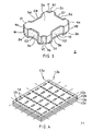
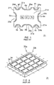
- a motherboard 31 shown in Fig. 6 is prepared first. More specifically, in constructing the motherboard, a conductive member is printed on or applied to a plurality of ceramic sheets (not shown). Then, circuit devices and wiring sections are provided. These sheets are then laminated to form the motherboard 31. The motherboard 31 is cut along boundaries 33a and 33b to produce a number of the individual substrates 21 shown in Fig. 5.
- the inner surfaces are connected to the wiring sections provided for each substrate 2 at its inside and on the surface.
- the motherboard 11 is cut along the boundaries 13a and 13b with a dicing saw to produce a plurality of the substrates 2.
- the through holes 14 and 15 are divided and the conductive member applied to the inner surfaces of the through holes 14 and 15 is thereby exposed to form the input terminals VB, VC, and M and the output terminal P at the respective corners of the substrate 2, and the ground terminals G1 to G4 at the respective side faces of the substrate 2, as shown in Fig. 2.
- the pegs 9 are soldered to the ground terminals G1 to G4 to mount the metal case 6 on the substrate 2, thereby completing the voltage-controlled oscillator 1.
Landscapes
- Inductance-Capacitance Distribution Constants And Capacitance-Resistance Oscillators (AREA)
- Lead Frames For Integrated Circuits (AREA)
- Shielding Devices Or Components To Electric Or Magnetic Fields (AREA)
Applications Claiming Priority (2)
| Application Number | Priority Date | Filing Date | Title |
|---|---|---|---|
| JP9090804A JPH10284935A (ja) | 1997-04-09 | 1997-04-09 | 電圧制御発振器およびその製造方法 |
| JP90804/97 | 1997-04-09 |
Publications (2)
| Publication Number | Publication Date |
|---|---|
| EP0871220A2 true EP0871220A2 (de) | 1998-10-14 |
| EP0871220A3 EP0871220A3 (de) | 1999-04-21 |
Family
ID=14008787
Family Applications (1)
| Application Number | Title | Priority Date | Filing Date |
|---|---|---|---|
| EP98302724A Withdrawn EP0871220A3 (de) | 1997-04-09 | 1998-04-07 | Pinbelegung eines Halbleitergehäuses |
Country Status (3)
| Country | Link |
|---|---|
| US (1) | US5966052A (de) |
| EP (1) | EP0871220A3 (de) |
| JP (1) | JPH10284935A (de) |
Cited By (8)
| Publication number | Priority date | Publication date | Assignee | Title |
|---|---|---|---|---|
| EP1050906A1 (de) * | 1999-05-06 | 2000-11-08 | Murata Manufacturing Co., Ltd. | Gehäuse für elektronische Bauteile |
| ES2150876A1 (es) * | 1999-01-14 | 2000-12-01 | Navarra Componentes Electro | Componente electrico de montaje superficial y rpocedimiento para su produccion. |
| GB2383207A (en) * | 2001-11-26 | 2003-06-18 | Murata Manufacturing Co | Oscillator module and electronic apparatus using the same |
| NL1016139C2 (nl) * | 1999-09-09 | 2004-08-03 | Rohm Co | Halfgeleiderchip en halfgeleiderinrichting welke deze gebruikt. |
| EP1480267A3 (de) * | 2003-05-23 | 2008-07-09 | Murata Manufacturing Co., Ltd. | Integrierte Elektronikkomponente |
| EP2712281A4 (de) * | 2011-05-19 | 2015-06-24 | Ngk Spark Plug Co | Verdrahtungssubstrat, mehrfach strukturiertes verdrahtungssubstrat und herstellungsverfahren dafür |
| EP3062590A4 (de) * | 2013-10-23 | 2017-05-24 | Kyocera Corporation | Leiterplatte und elektronische vorrichtung |
| EP4113589A3 (de) * | 2021-06-29 | 2023-05-03 | Shinko Electric Industries Co., Ltd. | Kopf für halbleitergehäuse und halbleitergehäuse |
Families Citing this family (59)
| Publication number | Priority date | Publication date | Assignee | Title |
|---|---|---|---|---|
| KR100259359B1 (ko) * | 1998-02-10 | 2000-06-15 | 김영환 | 반도체 패키지용 기판 및 반도체 패키지, 그리고 그 제조방법 |
| USD428604S (en) * | 1998-03-26 | 2000-07-25 | SII Quartz Techno Ltd. | Crystal oscillator |
| JP4783960B2 (ja) * | 1999-08-06 | 2011-09-28 | ミツミ電機株式会社 | 基板の保護装置 |
| DE19962231A1 (de) * | 1999-12-22 | 2001-07-12 | Infineon Technologies Ag | Verfahren zur Herstellung mikromechanischer Strukturen |
| JP4547781B2 (ja) * | 2000-07-28 | 2010-09-22 | パナソニック株式会社 | 多連チップ抵抗器の製造方法 |
| DE10053853A1 (de) * | 2000-10-30 | 2002-05-16 | Infineon Technologies Ag | Elektronisches Bauteil mit einer Abdeckungsvorrichtung und Herstellung derselben |
| JP2002141248A (ja) * | 2000-11-02 | 2002-05-17 | Murata Mfg Co Ltd | セラミック電子部品およびその製造方法 |
| US6760227B2 (en) * | 2000-11-02 | 2004-07-06 | Murata Manufacturing Co., Ltd. | Multilayer ceramic electronic component and manufacturing method thereof |
| JP2002164658A (ja) * | 2000-11-29 | 2002-06-07 | Sharp Corp | モジュール基板 |
| JP2002198460A (ja) * | 2000-12-27 | 2002-07-12 | Kyocera Corp | 多数個取り配線基板 |
| JP2003028649A (ja) * | 2001-05-11 | 2003-01-29 | Murata Mfg Co Ltd | センサ回路モジュールおよびそれを用いた電子装置 |
| JP2003163430A (ja) * | 2001-11-27 | 2003-06-06 | Nec Corp | プリント基板 |
| US7130198B2 (en) * | 2001-12-06 | 2006-10-31 | Rohm Co., Ltd. | Resin-packaged protection circuit module for rechargeable batteries and method of making the same |
| US6830959B2 (en) * | 2002-01-22 | 2004-12-14 | Fairchild Semiconductor Corporation | Semiconductor die package with semiconductor die having side electrical connection |
| US20040055782A1 (en) * | 2002-09-24 | 2004-03-25 | Alps Electric Co., Ltd. | Surface-mounting type electronic circuit unit having no melting of solder attaching electric part thereto |
| USD505397S1 (en) * | 2003-09-15 | 2005-05-24 | Nichia Corporation | Light emitting diode |
| JP4883882B2 (ja) * | 2003-09-25 | 2012-02-22 | 京セラ株式会社 | 電子装置 |
| USD508235S1 (en) * | 2003-12-05 | 2005-08-09 | Nichia Corporation | Light emitting diode |
| JP4301071B2 (ja) * | 2004-05-07 | 2009-07-22 | 株式会社村田製作所 | シールドケース付き電子部品およびその製造方法 |
| TWD112588S1 (zh) * | 2005-03-22 | 2006-08-21 | 羅姆電子股份有限公司 | 光電開關 |
| TWD112589S1 (zh) * | 2005-03-22 | 2006-08-21 | 羅姆電子股份有限公司 | 光電開關 |
| TWD112587S1 (zh) * | 2005-03-22 | 2006-08-21 | 羅姆電子股份有限公司 | 光電開關 |
| JP4918373B2 (ja) * | 2006-04-28 | 2012-04-18 | オリンパス株式会社 | 積層実装構造体 |
| JP3969453B1 (ja) * | 2006-05-17 | 2007-09-05 | 株式会社村田製作所 | ケース付き多層モジュール |
| JP4020149B1 (ja) * | 2006-06-19 | 2007-12-12 | 株式会社村田製作所 | 電子部品モジュール |
| JP4972391B2 (ja) | 2006-12-13 | 2012-07-11 | 新光電気工業株式会社 | シールドケース付パッケージおよびシールドケース付パッケージの製造方法 |
| TWM320181U (en) * | 2007-01-11 | 2007-10-01 | Everlight Electronics Co Ltd | Altenating current light emitting diode device |
| JP5446863B2 (ja) * | 2007-08-23 | 2014-03-19 | 株式会社大真空 | 電子部品用パッケージ及び電子部品用パッケージのベース |
| US8022511B2 (en) | 2008-02-05 | 2011-09-20 | Advanced Semiconductor Engineering, Inc. | Semiconductor device packages with electromagnetic interference shielding |
| US8212339B2 (en) * | 2008-02-05 | 2012-07-03 | Advanced Semiconductor Engineering, Inc. | Semiconductor device packages with electromagnetic interference shielding |
| US8350367B2 (en) | 2008-02-05 | 2013-01-08 | Advanced Semiconductor Engineering, Inc. | Semiconductor device packages with electromagnetic interference shielding |
| US7989928B2 (en) | 2008-02-05 | 2011-08-02 | Advanced Semiconductor Engineering Inc. | Semiconductor device packages with electromagnetic interference shielding |
| US8410584B2 (en) | 2008-08-08 | 2013-04-02 | Advanced Semiconductor Engineering, Inc. | Semiconductor device packages with electromagnetic interference shielding |
| TWI469278B (zh) * | 2008-08-21 | 2015-01-11 | 大真空股份有限公司 | A package for an electronic component, a substrate for packaging an electronic component, and a bonding structure between an electronic component package and a circuit substrate |
| US20100110656A1 (en) | 2008-10-31 | 2010-05-06 | Advanced Semiconductor Engineering, Inc. | Chip package and manufacturing method thereof |
| JP5218087B2 (ja) * | 2009-01-19 | 2013-06-26 | 三菱電機株式会社 | 半導体装置 |
| US8110902B2 (en) * | 2009-02-19 | 2012-02-07 | Advanced Semiconductor Engineering, Inc. | Chip package and manufacturing method thereof |
| US8212340B2 (en) * | 2009-07-13 | 2012-07-03 | Advanced Semiconductor Engineering, Inc. | Chip package and manufacturing method thereof |
| US8030750B2 (en) | 2009-11-19 | 2011-10-04 | Advanced Semiconductor Engineering, Inc. | Semiconductor device packages with electromagnetic interference shielding |
| US8368185B2 (en) * | 2009-11-19 | 2013-02-05 | Advanced Semiconductor Engineering, Inc. | Semiconductor device packages with electromagnetic interference shielding |
| US8378466B2 (en) | 2009-11-19 | 2013-02-19 | Advanced Semiconductor Engineering, Inc. | Wafer-level semiconductor device packages with electromagnetic interference shielding |
| US8569894B2 (en) | 2010-01-13 | 2013-10-29 | Advanced Semiconductor Engineering, Inc. | Semiconductor package with single sided substrate design and manufacturing methods thereof |
| TWI411075B (zh) | 2010-03-22 | 2013-10-01 | 日月光半導體製造股份有限公司 | 半導體封裝件及其製造方法 |
| TWI540698B (zh) | 2010-08-02 | 2016-07-01 | 日月光半導體製造股份有限公司 | 半導體封裝件與其製造方法 |
| US9406658B2 (en) | 2010-12-17 | 2016-08-02 | Advanced Semiconductor Engineering, Inc. | Embedded component device and manufacturing methods thereof |
| TWI525782B (zh) * | 2011-01-05 | 2016-03-11 | 矽品精密工業股份有限公司 | 半導體封裝件及其製法 |
| USD668658S1 (en) * | 2011-11-15 | 2012-10-09 | Connectblue Ab | Module |
| USD680119S1 (en) * | 2011-11-15 | 2013-04-16 | Connectblue Ab | Module |
| USD689053S1 (en) * | 2011-11-15 | 2013-09-03 | Connectblue Ab | Module |
| USD680545S1 (en) * | 2011-11-15 | 2013-04-23 | Connectblue Ab | Module |
| USD668659S1 (en) * | 2011-11-15 | 2012-10-09 | Connectblue Ab | Module |
| USD692896S1 (en) * | 2011-11-15 | 2013-11-05 | Connectblue Ab | Module |
| JP2013161831A (ja) * | 2012-02-01 | 2013-08-19 | Mitsumi Electric Co Ltd | 電子モジュール及びその製造方法 |
| US8704341B2 (en) | 2012-05-15 | 2014-04-22 | Advanced Semiconductor Engineering, Inc. | Semiconductor packages with thermal dissipation structures and EMI shielding |
| US8653634B2 (en) | 2012-06-11 | 2014-02-18 | Advanced Semiconductor Engineering, Inc. | EMI-shielded semiconductor devices and methods of making |
| US9583445B2 (en) * | 2014-03-18 | 2017-02-28 | Apple Inc. | Metal electromagnetic interference (EMI) shielding coating along an edge of a ceramic substrate |
| US20170127580A1 (en) * | 2014-06-10 | 2017-05-04 | Thomson Licensing | Set top box having paste-in-hole tuner shield |
| WO2020179458A1 (ja) * | 2019-03-07 | 2020-09-10 | 株式会社村田製作所 | 電子部品 |
| JP2020155517A (ja) * | 2019-03-19 | 2020-09-24 | キオクシア株式会社 | 半導体装置 |
Family Cites Families (5)
| Publication number | Priority date | Publication date | Assignee | Title |
|---|---|---|---|---|
| JPS5954247A (ja) * | 1982-09-21 | 1984-03-29 | Nec Corp | 電子部品 |
| JPS59198739A (ja) * | 1983-04-26 | 1984-11-10 | Nec Corp | チツプキヤリア |
| US4572757A (en) * | 1984-01-23 | 1986-02-25 | The Jade Corporation | Method of making a microcircuit substrate |
| SG48955A1 (en) * | 1992-07-27 | 1998-05-18 | Murata Manufacturing Co | Multilayer electronic component method of manufacturing the same and method of measuring characteristics thereof |
| JP3541491B2 (ja) * | 1994-06-22 | 2004-07-14 | セイコーエプソン株式会社 | 電子部品 |
-
1997
- 1997-04-09 JP JP9090804A patent/JPH10284935A/ja active Pending
-
1998
- 1998-04-07 EP EP98302724A patent/EP0871220A3/de not_active Withdrawn
- 1998-04-09 US US09/057,488 patent/US5966052A/en not_active Expired - Lifetime
Cited By (10)
| Publication number | Priority date | Publication date | Assignee | Title |
|---|---|---|---|---|
| ES2150876A1 (es) * | 1999-01-14 | 2000-12-01 | Navarra Componentes Electro | Componente electrico de montaje superficial y rpocedimiento para su produccion. |
| EP1050906A1 (de) * | 1999-05-06 | 2000-11-08 | Murata Manufacturing Co., Ltd. | Gehäuse für elektronische Bauteile |
| NL1016139C2 (nl) * | 1999-09-09 | 2004-08-03 | Rohm Co | Halfgeleiderchip en halfgeleiderinrichting welke deze gebruikt. |
| GB2383207A (en) * | 2001-11-26 | 2003-06-18 | Murata Manufacturing Co | Oscillator module and electronic apparatus using the same |
| GB2383207B (en) * | 2001-11-26 | 2003-12-24 | Murata Manufacturing Co | Oscillator module and electronic apparatus using the same |
| EP1480267A3 (de) * | 2003-05-23 | 2008-07-09 | Murata Manufacturing Co., Ltd. | Integrierte Elektronikkomponente |
| EP2712281A4 (de) * | 2011-05-19 | 2015-06-24 | Ngk Spark Plug Co | Verdrahtungssubstrat, mehrfach strukturiertes verdrahtungssubstrat und herstellungsverfahren dafür |
| EP3062590A4 (de) * | 2013-10-23 | 2017-05-24 | Kyocera Corporation | Leiterplatte und elektronische vorrichtung |
| EP4113589A3 (de) * | 2021-06-29 | 2023-05-03 | Shinko Electric Industries Co., Ltd. | Kopf für halbleitergehäuse und halbleitergehäuse |
| US12532589B2 (en) | 2021-06-29 | 2026-01-20 | Shinko Electric Industries Co., Ltd. | Header for semiconductor package, and semiconductor package |
Also Published As
| Publication number | Publication date |
|---|---|
| US5966052A (en) | 1999-10-12 |
| JPH10284935A (ja) | 1998-10-23 |
| EP0871220A3 (de) | 1999-04-21 |
Similar Documents
| Publication | Publication Date | Title |
|---|---|---|
| US5966052A (en) | Voltage-controlled oscillator with input and output on opposite corners of substrate | |
| JP3286917B2 (ja) | 電子部品用パッケージおよび電子部品 | |
| KR100676546B1 (ko) | 표면실장부품 | |
| US5227739A (en) | Voltage controlled oscillator having a resonator | |
| US6967537B2 (en) | Surface-mount crystal oscillator having an opened portion of the sidewalls | |
| US6674221B2 (en) | Electronic component module and piezoelectric oscillator device | |
| EP0872890A1 (de) | Hochfrequenzmodul | |
| CN101194418A (zh) | 电压控制型声表面波振荡器模块 | |
| JPH10215119A (ja) | 電圧制御発振器 | |
| US7049174B2 (en) | Method of manufacturing mounting substrate and surface mount crystal oscillator | |
| US5654676A (en) | Shielded VCO module having trimmable capacitor plate external to shield | |
| EP0910163B1 (de) | Oszillatorbaugruppe | |
| US20060170510A1 (en) | Mounting structure and method of surface-mount crystal oscillator | |
| JP2000004071A (ja) | 電子回路ユニット | |
| JP2001177346A (ja) | 圧電発振器 | |
| JP4228679B2 (ja) | 圧電発振器 | |
| EP0779708A2 (de) | Akustische Oberflächenwellenvorrichtung | |
| JP3099404B2 (ja) | 水晶発振器 | |
| JP2000151306A (ja) | 半導体装置 | |
| JP4204023B2 (ja) | 表面実装型圧電発振器 | |
| JPH066442Y2 (ja) | 蛍光表示管 | |
| KR100501193B1 (ko) | 수정발진기 | |
| JP2583990Y2 (ja) | 表面実装型圧電フィルタ | |
| JPH05152161A (ja) | 複合部品 | |
| JPH09186510A (ja) | 複合回路モジュール |
Legal Events
| Date | Code | Title | Description |
|---|---|---|---|
| PUAI | Public reference made under article 153(3) epc to a published international application that has entered the european phase |
Free format text: ORIGINAL CODE: 0009012 |
|
| 17P | Request for examination filed |
Effective date: 19980421 |
|
| AK | Designated contracting states |
Kind code of ref document: A2 Designated state(s): DE NL SE |
|
| AX | Request for extension of the european patent |
Free format text: AL;LT;LV;MK;RO;SI |
|
| PUAL | Search report despatched |
Free format text: ORIGINAL CODE: 0009013 |
|
| AK | Designated contracting states |
Kind code of ref document: A3 Designated state(s): AT BE CH CY DE DK ES FI FR GB GR IE IT LI LU MC NL PT SE |
|
| AX | Request for extension of the european patent |
Free format text: AL;LT;LV;MK;RO;SI |
|
| AKX | Designation fees paid |
Free format text: DE NL SE |
|
| 17Q | First examination report despatched |
Effective date: 20011122 |
|
| GRAP | Despatch of communication of intention to grant a patent |
Free format text: ORIGINAL CODE: EPIDOSNIGR1 |
|
| STAA | Information on the status of an ep patent application or granted ep patent |
Free format text: STATUS: THE APPLICATION IS DEEMED TO BE WITHDRAWN |
|
| 18D | Application deemed to be withdrawn |
Effective date: 20050830 |