EP0872882A2 - Méthode de fabrication d'un substrat incurvé de type métal-céramique - Google Patents
Méthode de fabrication d'un substrat incurvé de type métal-céramique Download PDFInfo
- Publication number
- EP0872882A2 EP0872882A2 EP98105261A EP98105261A EP0872882A2 EP 0872882 A2 EP0872882 A2 EP 0872882A2 EP 98105261 A EP98105261 A EP 98105261A EP 98105261 A EP98105261 A EP 98105261A EP 0872882 A2 EP0872882 A2 EP 0872882A2
- Authority
- EP
- European Patent Office
- Prior art keywords
- temperature
- ceramic
- plate
- metallization
- curved
- Prior art date
- Legal status (The legal status is an assumption and is not a legal conclusion. Google has not performed a legal analysis and makes no representation as to the accuracy of the status listed.)
- Withdrawn
Links
Images


Classifications
-
- H—ELECTRICITY
- H10—SEMICONDUCTOR DEVICES; ELECTRIC SOLID-STATE DEVICES NOT OTHERWISE PROVIDED FOR
- H10W—GENERIC PACKAGES, INTERCONNECTIONS, CONNECTORS OR OTHER CONSTRUCTIONAL DETAILS OF DEVICES COVERED BY CLASS H10
- H10W70/00—Package substrates; Interposers; Redistribution layers [RDL]
- H10W70/60—Insulating or insulated package substrates; Interposers; Redistribution layers
- H10W70/67—Insulating or insulated package substrates; Interposers; Redistribution layers characterised by their insulating layers or insulating parts
- H10W70/68—Shapes or dispositions thereof
-
- C—CHEMISTRY; METALLURGY
- C04—CEMENTS; CONCRETE; ARTIFICIAL STONE; CERAMICS; REFRACTORIES
- C04B—LIME, MAGNESIA; SLAG; CEMENTS; COMPOSITIONS THEREOF, e.g. MORTARS, CONCRETE OR LIKE BUILDING MATERIALS; ARTIFICIAL STONE; CERAMICS; REFRACTORIES; TREATMENT OF NATURAL STONE
- C04B37/00—Joining burned ceramic articles with other burned ceramic articles or other articles by heating
- C04B37/001—Joining burned ceramic articles with other burned ceramic articles or other articles by heating directly with other burned ceramic articles
-
- C—CHEMISTRY; METALLURGY
- C04—CEMENTS; CONCRETE; ARTIFICIAL STONE; CERAMICS; REFRACTORIES
- C04B—LIME, MAGNESIA; SLAG; CEMENTS; COMPOSITIONS THEREOF, e.g. MORTARS, CONCRETE OR LIKE BUILDING MATERIALS; ARTIFICIAL STONE; CERAMICS; REFRACTORIES; TREATMENT OF NATURAL STONE
- C04B37/00—Joining burned ceramic articles with other burned ceramic articles or other articles by heating
- C04B37/02—Joining burned ceramic articles with other burned ceramic articles or other articles by heating with metallic articles
- C04B37/021—Joining burned ceramic articles with other burned ceramic articles or other articles by heating with metallic articles in a direct manner, e.g. direct copper bonding [DCB]
-
- C—CHEMISTRY; METALLURGY
- C04—CEMENTS; CONCRETE; ARTIFICIAL STONE; CERAMICS; REFRACTORIES
- C04B—LIME, MAGNESIA; SLAG; CEMENTS; COMPOSITIONS THEREOF, e.g. MORTARS, CONCRETE OR LIKE BUILDING MATERIALS; ARTIFICIAL STONE; CERAMICS; REFRACTORIES; TREATMENT OF NATURAL STONE
- C04B37/00—Joining burned ceramic articles with other burned ceramic articles or other articles by heating
- C04B37/02—Joining burned ceramic articles with other burned ceramic articles or other articles by heating with metallic articles
- C04B37/023—Joining burned ceramic articles with other burned ceramic articles or other articles by heating with metallic articles characterised by the interlayer used
-
- H—ELECTRICITY
- H05—ELECTRIC TECHNIQUES NOT OTHERWISE PROVIDED FOR
- H05K—PRINTED CIRCUITS; CASINGS OR CONSTRUCTIONAL DETAILS OF ELECTRIC APPARATUS; MANUFACTURE OF ASSEMBLAGES OF ELECTRICAL COMPONENTS
- H05K3/00—Apparatus or processes for manufacturing printed circuits
- H05K3/0011—Working of insulating substrates or insulating layers
- H05K3/0014—Shaping of the substrate, e.g. by moulding
-
- H—ELECTRICITY
- H10—SEMICONDUCTOR DEVICES; ELECTRIC SOLID-STATE DEVICES NOT OTHERWISE PROVIDED FOR
- H10W—GENERIC PACKAGES, INTERCONNECTIONS, CONNECTORS OR OTHER CONSTRUCTIONAL DETAILS OF DEVICES COVERED BY CLASS H10
- H10W40/00—Arrangements for thermal protection or thermal control
- H10W40/20—Arrangements for cooling
- H10W40/25—Arrangements for cooling characterised by their materials
- H10W40/255—Arrangements for cooling characterised by their materials having a laminate or multilayered structure, e.g. direct bond copper [DBC] ceramic substrates
-
- H—ELECTRICITY
- H10—SEMICONDUCTOR DEVICES; ELECTRIC SOLID-STATE DEVICES NOT OTHERWISE PROVIDED FOR
- H10W—GENERIC PACKAGES, INTERCONNECTIONS, CONNECTORS OR OTHER CONSTRUCTIONAL DETAILS OF DEVICES COVERED BY CLASS H10
- H10W99/00—Subject matter not provided for in other groups of this subclass
-
- C—CHEMISTRY; METALLURGY
- C04—CEMENTS; CONCRETE; ARTIFICIAL STONE; CERAMICS; REFRACTORIES
- C04B—LIME, MAGNESIA; SLAG; CEMENTS; COMPOSITIONS THEREOF, e.g. MORTARS, CONCRETE OR LIKE BUILDING MATERIALS; ARTIFICIAL STONE; CERAMICS; REFRACTORIES; TREATMENT OF NATURAL STONE
- C04B2235/00—Aspects relating to ceramic starting mixtures or sintered ceramic products
- C04B2235/65—Aspects relating to heat treatments of ceramic bodies such as green ceramics or pre-sintered ceramics, e.g. burning, sintering or melting processes
- C04B2235/656—Aspects relating to heat treatments of ceramic bodies such as green ceramics or pre-sintered ceramics, e.g. burning, sintering or melting processes characterised by specific heating conditions during heat treatment
- C04B2235/6562—Heating rate
-
- C—CHEMISTRY; METALLURGY
- C04—CEMENTS; CONCRETE; ARTIFICIAL STONE; CERAMICS; REFRACTORIES
- C04B—LIME, MAGNESIA; SLAG; CEMENTS; COMPOSITIONS THEREOF, e.g. MORTARS, CONCRETE OR LIKE BUILDING MATERIALS; ARTIFICIAL STONE; CERAMICS; REFRACTORIES; TREATMENT OF NATURAL STONE
- C04B2235/00—Aspects relating to ceramic starting mixtures or sintered ceramic products
- C04B2235/65—Aspects relating to heat treatments of ceramic bodies such as green ceramics or pre-sintered ceramics, e.g. burning, sintering or melting processes
- C04B2235/656—Aspects relating to heat treatments of ceramic bodies such as green ceramics or pre-sintered ceramics, e.g. burning, sintering or melting processes characterised by specific heating conditions during heat treatment
- C04B2235/6565—Cooling rate
-
- C—CHEMISTRY; METALLURGY
- C04—CEMENTS; CONCRETE; ARTIFICIAL STONE; CERAMICS; REFRACTORIES
- C04B—LIME, MAGNESIA; SLAG; CEMENTS; COMPOSITIONS THEREOF, e.g. MORTARS, CONCRETE OR LIKE BUILDING MATERIALS; ARTIFICIAL STONE; CERAMICS; REFRACTORIES; TREATMENT OF NATURAL STONE
- C04B2237/00—Aspects relating to ceramic laminates or to joining of ceramic articles with other articles by heating
- C04B2237/02—Aspects relating to interlayers, e.g. used to join ceramic articles with other articles by heating
- C04B2237/12—Metallic interlayers
- C04B2237/124—Metallic interlayers based on copper
-
- C—CHEMISTRY; METALLURGY
- C04—CEMENTS; CONCRETE; ARTIFICIAL STONE; CERAMICS; REFRACTORIES
- C04B—LIME, MAGNESIA; SLAG; CEMENTS; COMPOSITIONS THEREOF, e.g. MORTARS, CONCRETE OR LIKE BUILDING MATERIALS; ARTIFICIAL STONE; CERAMICS; REFRACTORIES; TREATMENT OF NATURAL STONE
- C04B2237/00—Aspects relating to ceramic laminates or to joining of ceramic articles with other articles by heating
- C04B2237/30—Composition of layers of ceramic laminates or of ceramic or metallic articles to be joined by heating, e.g. Si substrates
- C04B2237/32—Ceramic
- C04B2237/34—Oxidic
- C04B2237/343—Alumina or aluminates
-
- C—CHEMISTRY; METALLURGY
- C04—CEMENTS; CONCRETE; ARTIFICIAL STONE; CERAMICS; REFRACTORIES
- C04B—LIME, MAGNESIA; SLAG; CEMENTS; COMPOSITIONS THEREOF, e.g. MORTARS, CONCRETE OR LIKE BUILDING MATERIALS; ARTIFICIAL STONE; CERAMICS; REFRACTORIES; TREATMENT OF NATURAL STONE
- C04B2237/00—Aspects relating to ceramic laminates or to joining of ceramic articles with other articles by heating
- C04B2237/30—Composition of layers of ceramic laminates or of ceramic or metallic articles to be joined by heating, e.g. Si substrates
- C04B2237/32—Ceramic
- C04B2237/36—Non-oxidic
- C04B2237/365—Silicon carbide
-
- C—CHEMISTRY; METALLURGY
- C04—CEMENTS; CONCRETE; ARTIFICIAL STONE; CERAMICS; REFRACTORIES
- C04B—LIME, MAGNESIA; SLAG; CEMENTS; COMPOSITIONS THEREOF, e.g. MORTARS, CONCRETE OR LIKE BUILDING MATERIALS; ARTIFICIAL STONE; CERAMICS; REFRACTORIES; TREATMENT OF NATURAL STONE
- C04B2237/00—Aspects relating to ceramic laminates or to joining of ceramic articles with other articles by heating
- C04B2237/30—Composition of layers of ceramic laminates or of ceramic or metallic articles to be joined by heating, e.g. Si substrates
- C04B2237/32—Ceramic
- C04B2237/36—Non-oxidic
- C04B2237/366—Aluminium nitride
-
- C—CHEMISTRY; METALLURGY
- C04—CEMENTS; CONCRETE; ARTIFICIAL STONE; CERAMICS; REFRACTORIES
- C04B—LIME, MAGNESIA; SLAG; CEMENTS; COMPOSITIONS THEREOF, e.g. MORTARS, CONCRETE OR LIKE BUILDING MATERIALS; ARTIFICIAL STONE; CERAMICS; REFRACTORIES; TREATMENT OF NATURAL STONE
- C04B2237/00—Aspects relating to ceramic laminates or to joining of ceramic articles with other articles by heating
- C04B2237/30—Composition of layers of ceramic laminates or of ceramic or metallic articles to be joined by heating, e.g. Si substrates
- C04B2237/40—Metallic
- C04B2237/407—Copper
-
- C—CHEMISTRY; METALLURGY
- C04—CEMENTS; CONCRETE; ARTIFICIAL STONE; CERAMICS; REFRACTORIES
- C04B—LIME, MAGNESIA; SLAG; CEMENTS; COMPOSITIONS THEREOF, e.g. MORTARS, CONCRETE OR LIKE BUILDING MATERIALS; ARTIFICIAL STONE; CERAMICS; REFRACTORIES; TREATMENT OF NATURAL STONE
- C04B2237/00—Aspects relating to ceramic laminates or to joining of ceramic articles with other articles by heating
- C04B2237/50—Processing aspects relating to ceramic laminates or to the joining of ceramic articles with other articles by heating
- C04B2237/54—Oxidising the surface before joining
-
- C—CHEMISTRY; METALLURGY
- C04—CEMENTS; CONCRETE; ARTIFICIAL STONE; CERAMICS; REFRACTORIES
- C04B—LIME, MAGNESIA; SLAG; CEMENTS; COMPOSITIONS THEREOF, e.g. MORTARS, CONCRETE OR LIKE BUILDING MATERIALS; ARTIFICIAL STONE; CERAMICS; REFRACTORIES; TREATMENT OF NATURAL STONE
- C04B2237/00—Aspects relating to ceramic laminates or to joining of ceramic articles with other articles by heating
- C04B2237/50—Processing aspects relating to ceramic laminates or to the joining of ceramic articles with other articles by heating
- C04B2237/70—Forming laminates or joined articles comprising layers of a specific, unusual thickness
-
- C—CHEMISTRY; METALLURGY
- C04—CEMENTS; CONCRETE; ARTIFICIAL STONE; CERAMICS; REFRACTORIES
- C04B—LIME, MAGNESIA; SLAG; CEMENTS; COMPOSITIONS THEREOF, e.g. MORTARS, CONCRETE OR LIKE BUILDING MATERIALS; ARTIFICIAL STONE; CERAMICS; REFRACTORIES; TREATMENT OF NATURAL STONE
- C04B2237/00—Aspects relating to ceramic laminates or to joining of ceramic articles with other articles by heating
- C04B2237/50—Processing aspects relating to ceramic laminates or to the joining of ceramic articles with other articles by heating
- C04B2237/76—Forming laminates or joined articles comprising at least one member in the form other than a sheet or disc, e.g. two tubes or a tube and a sheet or disc
-
- C—CHEMISTRY; METALLURGY
- C04—CEMENTS; CONCRETE; ARTIFICIAL STONE; CERAMICS; REFRACTORIES
- C04B—LIME, MAGNESIA; SLAG; CEMENTS; COMPOSITIONS THEREOF, e.g. MORTARS, CONCRETE OR LIKE BUILDING MATERIALS; ARTIFICIAL STONE; CERAMICS; REFRACTORIES; TREATMENT OF NATURAL STONE
- C04B2237/00—Aspects relating to ceramic laminates or to joining of ceramic articles with other articles by heating
- C04B2237/50—Processing aspects relating to ceramic laminates or to the joining of ceramic articles with other articles by heating
- C04B2237/82—Two substrates not completely covering each other, e.g. two plates in a staggered position
-
- H—ELECTRICITY
- H05—ELECTRIC TECHNIQUES NOT OTHERWISE PROVIDED FOR
- H05K—PRINTED CIRCUITS; CASINGS OR CONSTRUCTIONAL DETAILS OF ELECTRIC APPARATUS; MANUFACTURE OF ASSEMBLAGES OF ELECTRICAL COMPONENTS
- H05K1/00—Printed circuits
- H05K1/02—Details
- H05K1/03—Use of materials for the substrate
- H05K1/0306—Inorganic insulating substrates, e.g. ceramic, glass
-
- H—ELECTRICITY
- H05—ELECTRIC TECHNIQUES NOT OTHERWISE PROVIDED FOR
- H05K—PRINTED CIRCUITS; CASINGS OR CONSTRUCTIONAL DETAILS OF ELECTRIC APPARATUS; MANUFACTURE OF ASSEMBLAGES OF ELECTRICAL COMPONENTS
- H05K2201/00—Indexing scheme relating to printed circuits covered by H05K1/00
- H05K2201/09—Shape and layout
- H05K2201/09009—Substrate related
- H05K2201/09018—Rigid curved substrate
-
- H—ELECTRICITY
- H05—ELECTRIC TECHNIQUES NOT OTHERWISE PROVIDED FOR
- H05K—PRINTED CIRCUITS; CASINGS OR CONSTRUCTIONAL DETAILS OF ELECTRIC APPARATUS; MANUFACTURE OF ASSEMBLAGES OF ELECTRICAL COMPONENTS
- H05K2203/00—Indexing scheme relating to apparatus or processes for manufacturing printed circuits covered by H05K3/00
- H05K2203/11—Treatments characterised by their effect, e.g. heating, cooling, roughening
- H05K2203/1105—Heating or thermal processing not related to soldering, firing, curing or laminating, e.g. for shaping the substrate or during finish plating
-
- H—ELECTRICITY
- H05—ELECTRIC TECHNIQUES NOT OTHERWISE PROVIDED FOR
- H05K—PRINTED CIRCUITS; CASINGS OR CONSTRUCTIONAL DETAILS OF ELECTRIC APPARATUS; MANUFACTURE OF ASSEMBLAGES OF ELECTRICAL COMPONENTS
- H05K2203/00—Indexing scheme relating to apparatus or processes for manufacturing printed circuits covered by H05K3/00
- H05K2203/30—Details of processes not otherwise provided for in H05K2203/01 - H05K2203/17
- H05K2203/302—Bending a rigid substrate; Breaking rigid substrates by bending
-
- H—ELECTRICITY
- H10—SEMICONDUCTOR DEVICES; ELECTRIC SOLID-STATE DEVICES NOT OTHERWISE PROVIDED FOR
- H10W—GENERIC PACKAGES, INTERCONNECTIONS, CONNECTORS OR OTHER CONSTRUCTIONAL DETAILS OF DEVICES COVERED BY CLASS H10
- H10W90/00—Package configurations
- H10W90/701—Package configurations characterised by the relative positions of pads or connectors relative to package parts
- H10W90/751—Package configurations characterised by the relative positions of pads or connectors relative to package parts of bond wires
- H10W90/754—Package configurations characterised by the relative positions of pads or connectors relative to package parts of bond wires between a chip and a stacked insulating package substrate, interposer or RDL
-
- Y—GENERAL TAGGING OF NEW TECHNOLOGICAL DEVELOPMENTS; GENERAL TAGGING OF CROSS-SECTIONAL TECHNOLOGIES SPANNING OVER SEVERAL SECTIONS OF THE IPC; TECHNICAL SUBJECTS COVERED BY FORMER USPC CROSS-REFERENCE ART COLLECTIONS [XRACs] AND DIGESTS
- Y10—TECHNICAL SUBJECTS COVERED BY FORMER USPC
- Y10T—TECHNICAL SUBJECTS COVERED BY FORMER US CLASSIFICATION
- Y10T29/00—Metal working
- Y10T29/49—Method of mechanical manufacture
- Y10T29/49002—Electrical device making
- Y10T29/49117—Conductor or circuit manufacturing
- Y10T29/49124—On flat or curved insulated base, e.g., printed circuit, etc.
- Y10T29/49128—Assembling formed circuit to base
-
- Y—GENERAL TAGGING OF NEW TECHNOLOGICAL DEVELOPMENTS; GENERAL TAGGING OF CROSS-SECTIONAL TECHNOLOGIES SPANNING OVER SEVERAL SECTIONS OF THE IPC; TECHNICAL SUBJECTS COVERED BY FORMER USPC CROSS-REFERENCE ART COLLECTIONS [XRACs] AND DIGESTS
- Y10—TECHNICAL SUBJECTS COVERED BY FORMER USPC
- Y10T—TECHNICAL SUBJECTS COVERED BY FORMER US CLASSIFICATION
- Y10T29/00—Metal working
- Y10T29/49—Method of mechanical manufacture
- Y10T29/49002—Electrical device making
- Y10T29/49117—Conductor or circuit manufacturing
- Y10T29/49124—On flat or curved insulated base, e.g., printed circuit, etc.
- Y10T29/49147—Assembling terminal to base
-
- Y—GENERAL TAGGING OF NEW TECHNOLOGICAL DEVELOPMENTS; GENERAL TAGGING OF CROSS-SECTIONAL TECHNOLOGIES SPANNING OVER SEVERAL SECTIONS OF THE IPC; TECHNICAL SUBJECTS COVERED BY FORMER USPC CROSS-REFERENCE ART COLLECTIONS [XRACs] AND DIGESTS
- Y10—TECHNICAL SUBJECTS COVERED BY FORMER USPC
- Y10T—TECHNICAL SUBJECTS COVERED BY FORMER US CLASSIFICATION
- Y10T29/00—Metal working
- Y10T29/49—Method of mechanical manufacture
- Y10T29/49002—Electrical device making
- Y10T29/49117—Conductor or circuit manufacturing
- Y10T29/49124—On flat or curved insulated base, e.g., printed circuit, etc.
- Y10T29/49155—Manufacturing circuit on or in base
- Y10T29/49158—Manufacturing circuit on or in base with molding of insulated base
Definitions
- the invention relates to a method for producing a curved metal-ceramic substrate for use as a substrate in electrical or electronic Circuits or components according to the preamble of claim 1.
- this layer or this coating forms a eutectic with a melting temperature below the melting temperature of the metal (for example copper), so that it can be connected to one another by laying the foil on the ceramic and by heating all the layers, specifically by melting the metal or copper only in the area of the melting layer or oxide layer.
- a curved substrate and its production are known (EP 0 279 601).
- the metal layer on the concavely curved upper side of the ceramic layer has a significantly greater thickness than the metal layer on the convexly curved underside of the substrate.
- This design is necessary in the known case, since there the curvature of the substrate is to be achieved during cooling after the DCB process, with which the two metallizations are attached to the ceramic layer or ceramic plate. Since the metallization on the upper side has a greater thickness and thus a larger volume, thermally induced stresses on the upper side are greater than on the underside, so that the substrate bulges in the aforementioned manner when it cools.
- the object of the invention is to demonstrate a method with which curved metal-ceramic substrates in particular with the same thickness of the metallizations on the Top and bottom can be easily manufactured. To solve this The object is a method according to claim 1.
- the metal-ceramic substrate produced by the method according to the invention is for suitable and has electrical or electronic power circuits or modules an improved, temperature-independent compared to known curved substrates Heat dissipation.
- the method according to the invention provides, initially from a plan or in essentially plan to manufacture a pre-curved ceramic plate and blank then on this bulging ceramic plate in a further process section To apply metallization.
- the curvature of the substrate or the ceramic layer Due to the curvature of the substrate or the ceramic layer, this is possible in the Use to bend elastically so flat that the substrate due to elastic tension of the ceramic layer tightly and firmly against a surface of heat dissipative metal plate is present, and thereby improved heat dissipation results, especially when using a cooling paste between the substrate and the metal plate.
- the curvature of the substrate thus serves, in particular, for a optimal placement of the underside or the lower metallization of the substrate on e.g. a metal plate and thus the best possible heat transfer between the Substrate and this, for example, a metal plate forming a heat sink guarantee.
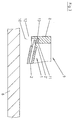
- the substrate 1 shown in the figures consists essentially of a Ceramic layer or ceramic plate 2, for example an aluminum oxide ceramic and that on both surface sides, each with a metallization 3 or 4 is provided.
- the metallizations 3 and 4 are each formed by a copper foil, with the help of the DCB technology known to the person skilled in the art Ceramic layer 2 is connected.
- the metallizations have the same thickness.
- the ceramic layer 2 has a top view rectangular cut with the longer longitudinal axis L and perpendicular to it running shorter transverse axis Q.
- the ceramic layer 2 is in the illustrated Embodiment arched or curved around an axis parallel to the transverse axis, see above that the top of the ceramic layer 2 is concave and the bottom is convex.
- the metallizations 3 and 4 there are curved in the same way.
- the The axis of curvature is indicated by Q 'in FIG. 1, but actually has one much greater distance from the substrate 1 than shown in this figure.
- the Metallization 3 on the top is structured and forms conductor tracks as well Contact surfaces, the latter in particular also for fastening, e.g. for soldering of electronic components 5.
- the metallization 4 on the underside is continuous educated.
- the curvature of the ceramic layer 2 is such that when the substrate with the lower metallization 4 in the middle between the two perpendicular to the longitudinal axis L. and transverse sides 2 'lying parallel to the axis of curvature Q' on a flat surface, for example on the top of a flat metal plate 6, the bottom of the Ceramic layer 2 on each transverse side 2 'a distance x from the top of the Has metal plate 6. In the embodiment shown, this distance is x for example about 0.1-0.8% of the length that the curved ceramic layer 2 between the two sides 2 ', plus the thickness of the lower Metallization 4.
- the thermal conductivity between the substrate 1 and the Metal plate 6, which is part of a heat sink or a housing, for example is, can be significantly improved.
- the substrate 1 is on the top with a layer of a cooling paste 7 provided plate 6 and then on the edge and thus also pressed on the narrow sides 2 'on the plate 6, whereby by the elastic deformation of the ceramic layer 2 a tight fit of the lower Metallization 4 on the metal plate 6 and even distribution of the cooling paste 7 over the entire area occupied by the lower metal coating 4 Metal plate 6 is done.
- the ceramic layer 2 without problems, in particular also can be bent back into a flat shape without the risk of breakage, and even if the top, on the concave side of the ceramic layer provided metallization 3 is structured and thus at least in large part the top of the ceramic layer does not form a continuous metallization, but in the axis direction perpendicular to the axis of curvature only short dimensions having.
- About the upper metallization 3 can thus when bending back Substrate 1 in the flat shape also no excessively high tensile forces between the Ceramic layer 2 and the metallization 3 occur.
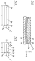
- Fig. 3 shows the clamping of the substrate 1 at the edge, i.e. especially in Area of the two narrow sides 2 'on the one forming a rectangular frame Part 8 of a housing 9, with which the substrate 1 then on the part of the heat sink forming plate 6 can be attached using the cooling paste 7.
- the housing part 8 has a fold-like Recess 10, which i.a. a contact surface 11 for supporting the top of the Forms ceramic layer 2 in the region of the edge.
- the fold or contact surface 11, however the underside 12 of the housing part 8 also have a curved course, and in accordance with the curvature of the substrate 1 or the ceramic layer 2.
- the edge or the bottom 12 is on the same level with the bottom of the Metallization 4.
- an intermediate layer 13 made of a permanently elastic mass, preferably one permanently elastic adhesive provided.
- an improved heat transfer between the substrate 1 and the metal plate 6 also has the advantage that stresses between the substrate 1 and the housing 9 are avoided, especially when installing the Substrate 1 on the housing 9. Only when it is attached to the metal plate 6 are the Substrate 1 and the housing 9 elastically deformed.
- Figure 5 Another possible execution is shown in Figure 5. In this version, the upper metallization 3 is sufficient the edge of the ceramic layer 2 and thus lies against the fold surface 11.
- the substrate 1 is curved only about the axis Q '.
- the substrate is also possible to design the substrate so that it is two Axes running perpendicular to each other, namely around the axis Q 'parallel to the Transverse axis Q and at the same time is curved around an axis parallel to the longitudinal axis L, again concave about both axes at the top, so that the substrate for example, a convex on the underside or on the metallization 4 there has a curved surface corresponding to a partial surface of a spherical surface.
- the substrate was a rectangular cut, i.e. in plan view a rectangular shape having.
- Other shapes are also conceivable for the substrate, for example that in FIG Figure 4 reproduced substrate 14, the shape of which is a rectangular or square green form with protrusions on two opposite sides composed, or the rectangular substrate 15 with rounded and / or chamfered corners and / or the round substrate 16.
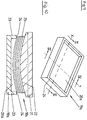
- a molding tool 18 which consists essentially of a sintered or molded plate 19 from a heat-resistant material, for example made of silicon carbide (SiC) and on has a mold cavity or depression 20 on its upper side, which is shown in FIG Embodiment about two mutually perpendicular axes that are parallel to the Longitudinal axis and transverse axis of the mold plate 19 are.
- the longitudinal axis is at the 7 with the X axis and the transverse axis with the Y axis.
- the Depth t of the mold cavity 20 in the direction perpendicular to the X axis and Y axis running Z axis is, for example, 0.05-1.5% of the width of the B or else the Length L.
- the depth t is, for example, 1 mm.
- a separating powder, e.g. corundum powder, is located between the blanks 2a.
- the Plate blanks 2a are, for example, made of a green ceramic extruded or otherwise shaped material made by punching.
- the Dimensions of the blanks 2a are slightly smaller than the dimensions of the mold plate 19.
- the blanks 2a Because of the dead weight of the blanks, they lie against each other and the lowest blank against the surface formed by the mold cavity 20. At a sufficiently high temperature, for example at 1350 ° C, the blanks 2a then sintered or fired in a normal atmosphere so that after the burner arched ceramic plates 2 are obtained.
- the fired ceramic plates 2 are slowly cooled to room temperature, with a cooling rate or a decrease in temperature of about 3 ° C. per minute.
- the individual, curved ceramic plates 2 are removed from the stack and then each provided with the metallizations 3 and 4.
- an oxidized copper foil for example forming the metallization 3, with a thickness of 0.3 mm is placed on one side of each curved ceramic layer 2. This is followed by heating to 1072 ° C in a nitrogen atmosphere with an oxygen content of 35 ppm.
- the curved ceramic plate and the copper foil which is then tightly lying on it and becomes soft due to the heating, but is only molten in the area of the eutectic formed by the copper oxide layer, are used for about six Minutes kept at the temperature of 1072 ° C.
- This is then cooled to room temperature and the metallization is applied to the other surface side of the ceramic plate 2, for example the metallization 4, in the same way.
- the structuring of at least one metallization takes place with the aid of a masking and etching technique, namely for example the metallization 3.
- an etching mask is applied to this metallization.
- the etching then takes place with a suitable etching agent, for example FeCl 3 . After the etching, the etching mask is removed.
- the substrates then produced have metallizations 3 and 4 of the same thickness and for example a bulge of the order of 0.5-6 mm.
- a weight plate 21 is placed on the stack of the blank 2a put on, which are also made of a temperature-resistant material, for example Sintered material, e.g. Silicon carbide (SiC) exists.
- the weight plate forms on the Underside of a surface 22, the shape of the geometry of the shaped surface of the trough 20th corresponds.
- this weight plate 21 is shown so that the Length dimension L 'is approximately the length L of the mold plate, with the Width dimension of the weight plate 21 is approximately the width B of the molding plate 19 corresponds.
- the length L 'and / or the Width B 'of the weight plate 21 deviates from the length L or the width B, i.e. is much smaller or much larger.
- the length L ' in the range between 0.2 - 200% of L.
- the area of the mold trough 20 is curved. Basically, there is also the possibility that the area of a plurality of successive stages is formed.
- the curved or curved ceramic plate 2 is curved around two mutually perpendicular spatial axes. It understands It is evident that substrates are also produced with the method described can be, each one curved around only one spatial axis Have ceramic layer or ceramic plate.
- the trough 20 is concave only about an axial direction, and for example as a cylindrical surface and not as a spherical surface.
- the stack is extended onto a shaped plate which is concave only around an axis the plate blanks 2a and then after complaining with the Weight plate 21 in the manner described above at a sufficient temperature sintered or pre-fired, for example at a temperature of about 1350 ° C. It is then cooled to room temperature and the stack is placed on top from the pre-fired plate blanks 1 'onto a new shaped plate which is similar to the 9 has a mold cavity 20 which e.g. again only by one Axis is concave.
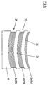
- FIGS. 10-13 show a molding tool 18a and one with this molding tool carried out process for the production of curved ceramic plates 2.
- Das Molding tool 18a consists of a molding plate 19a and a weighting plate 21.
- the mold plate 19a forms on its upper side the concave mold cavity 20a a depression is realized, which has a substantially constant depth t ', by a closed, circumferential edge 23 and a substantially flat Floor is limited.
- the depth t ' is again approximately 0.05-1.5% of the length L or width B.
- the edge 23 forms a mold cavity 20a enclosing edge surface 24 with a constant width b, which is about 0.2-20% in length L or width B corresponds.
- a stack of plate blanks 2b is placed on the molding plate 19a in such a way that the bottom blank 2b rests with its peripheral edge on the edge 23, approximately over a width of 3 mm.
- the stack contains, for example, a total of fifty blanks 2b, each blank 2b having a rectangular cut with a length of 150 mm and a width of 100 mm.
- the blanks 2b are fired flat ceramic plates (Al 2 0 3 96%).
- the weight plate 21 is placed on the stack. Then the stack is on 1200 ° C with a heating rate of about 2 ° C / minute and then about kept at 1200 ° C for five hours. Then it cools down Room temperature with a cooling rate of approx. 2 ° C / minute.
- the cooled ceramic plates then surprisingly have a curvature in two perpendicular spatial axes.
- Process steps the application of the metallizations 3 and 4 namely for example, first the application of the metallization 3 by placing one oxidized copper foil with a thickness of 0.3 mm on the concave curved top the respective pre-curved ceramic plate 2, which is then together with this copper foil in a nitrogen atmosphere with an oxygen content of approx. 35 ppm heated to 1072 ° C and for example for six minutes at this temperature held and then cooled to room temperature.
- the metallization 4 is applied in an analogous manner using an oxidized copper foil. Then at least one of the two metallizations, for example the metallization 3, is structured by means of the masking and etching technique, for which an etching mask is applied and then the etching is carried out with a suitable etching agent, for example with FeCl 3 . The etching mask is then removed.
- a suitable etching agent for example with FeCl 3
- This method can be modified in such a way that the production of the curved ceramic plates 2 takes place in two steps, for example under Use of a molding plate 19a, similar to that of FIG. 12, only on two opposite sides has the upwardly projecting edge 23, so that the Blanks 2b in this first step only with two opposite one another Edge areas rest on the edges 23 and in the first method step only be arched around a spatial axis.
- the blanks are then after the first process step or after the first heat treatment to room temperature cooled and placed on a further molding plate for a second process step, which in turn is similar to the representation of FIG. 13 only on two each other opposite sides has the edge 23, in such a way that the blanks now rest with their other two edge areas on the edges 23.
- the heating rate of, for example, 2 ° C./minute and keeping the Blanks at a temperature of approx. 1200 ° C for a sufficient period of time, for example five hours and then a slow cool down with one Cooling speed from approx. 2 ° C / minute to room temperature.
- the metallizations 3 and 4 can also be applied in other ways, for example by printing the curved ceramic plate 2 with a solder paste, for example with a solder paste consisting of 40% Ag, 55% Cu and 5% Ti both on the top and bottom of the ceramic plate 2.
- a solder paste for example with a solder paste consisting of 40% Ag, 55% Cu and 5% Ti both on the top and bottom of the ceramic plate 2.
- the method step involves contacting the ceramic layer on both sides with one each Copper foil with a thickness of 0.3 mm and then heating the whole Arrange in vacuum at about 850 ° C and hold the array over one sufficient time, for example eight minutes at this temperature. It is then cooled to room temperature. Subsequently, in the Structuring at least one metallization described above respectively.
- the substrates are a Have a bulge of 0.5 - 0.6 mm.
- solder foil is, for example, a thin copper foil which is oxidized on both sides and which is placed between the curved ceramic plate 2 and the copper foil forming the respective metallization the assembly is heated to a temperature of, for example, 1072 ° C.
- the copper foil is connected to the ceramic by melting the solder foil, and the metallization is carried out using the solder foil and the copper foils forming the metallizations can again be made here in two successive steps, firstly on one side, for example for producing the metallization 3, and then for the other side, for example for producing the metallization 4.
- FIG. 14 Another possibility for producing the curved ceramic plates 2 from the Blanks 2a or 2b is shown in FIG. 14.
- a molding plate 19 used, on which a first stack 25 of blanks 2a or 2b is applied.
- a further shaped or sintered plate 26 which is on it Top of the mold surface or mold cavity of the mold plate 19 correspondingly concave is shaped and is correspondingly convex on its underside.
- On this second one Stack 25 a second mold plate 26 is arranged on which a third stack 25 extends Blanks 2a or 2b is located.
- the mold plates 26 in turn consist of the heat-resistant material, namely sintered material, for example silicon carbide.
- Silicon carbide is suitable for the molding plate 19 or 19a and the weighting plate 21 or another material, which by the heat treatment or Burning forces and temperatures are not deformable.
Landscapes
- Chemical & Material Sciences (AREA)
- Engineering & Computer Science (AREA)
- Ceramic Engineering (AREA)
- Materials Engineering (AREA)
- Structural Engineering (AREA)
- Organic Chemistry (AREA)
- Manufacturing & Machinery (AREA)
- Microelectronics & Electronic Packaging (AREA)
- Ceramic Products (AREA)
- Cooling Or The Like Of Semiconductors Or Solid State Devices (AREA)
- Structure Of Printed Boards (AREA)
- Laminated Bodies (AREA)
Applications Claiming Priority (2)
| Application Number | Priority Date | Filing Date | Title |
|---|---|---|---|
| DE19715540A DE19715540C2 (de) | 1997-04-15 | 1997-04-15 | Verfahren zum Herstellen eines gewölbten Metall-Keramik-Substrates |
| DE19715540 | 1997-04-15 |
Publications (2)
| Publication Number | Publication Date |
|---|---|
| EP0872882A2 true EP0872882A2 (fr) | 1998-10-21 |
| EP0872882A3 EP0872882A3 (fr) | 1999-04-21 |
Family
ID=7826465
Family Applications (1)
| Application Number | Title | Priority Date | Filing Date |
|---|---|---|---|
| EP98105261A Withdrawn EP0872882A3 (fr) | 1997-04-15 | 1998-03-24 | Méthode de fabrication d'un substrat incurvé de type métal-céramique |
Country Status (3)
| Country | Link |
|---|---|
| US (1) | US6345437B1 (fr) |
| EP (1) | EP0872882A3 (fr) |
| DE (1) | DE19715540C2 (fr) |
Cited By (2)
| Publication number | Priority date | Publication date | Assignee | Title |
|---|---|---|---|---|
| CN103339723A (zh) * | 2011-02-08 | 2013-10-02 | 富士电机株式会社 | 半导体模块用散热板的制造方法、该散热板以及使用该散热板的半导体模块 |
| EP3177580A1 (fr) * | 2014-08-05 | 2017-06-14 | Heraeus Deutschland GmbH & Co. KG | Procédé de production de substrats céramique métallisés sur deux faces |
Families Citing this family (8)
| Publication number | Priority date | Publication date | Assignee | Title |
|---|---|---|---|---|
| DE19942915A1 (de) * | 1999-09-08 | 2001-03-15 | Still Gmbh | Leistungshalbleitermodul |
| JP4692708B2 (ja) | 2002-03-15 | 2011-06-01 | Dowaメタルテック株式会社 | セラミックス回路基板およびパワーモジュール |
| GB0805021D0 (en) * | 2008-03-18 | 2008-04-16 | Renishaw Plc | Apparatus and method for electronic circuit manufacture |
| CN102355798B (zh) * | 2011-10-25 | 2014-04-23 | 中国兵器工业集团第二一四研究所苏州研发中心 | 柱面模块电路板的制作方法以及烧结支架 |
| CN103794571B (zh) * | 2014-01-25 | 2017-01-04 | 嘉兴斯达半导体股份有限公司 | 一种功率半导体用新型金属-陶瓷绝缘基板 |
| JP6361532B2 (ja) * | 2015-03-10 | 2018-07-25 | 三菱マテリアル株式会社 | 放熱板付パワーモジュール用基板の製造方法 |
| KR101953433B1 (ko) * | 2016-03-07 | 2019-02-28 | 주식회사 케이씨씨 | 세라믹 기판 휨 발생용 도구 세트 및 이를 이용한 세라믹 기판의 휨 발생 방법 |
| US11764077B2 (en) * | 2021-07-23 | 2023-09-19 | Innolux Corporation | Composite layer circuit element and manufacturing method thereof |
Family Cites Families (12)
| Publication number | Priority date | Publication date | Assignee | Title |
|---|---|---|---|---|
| US3766634A (en) * | 1972-04-20 | 1973-10-23 | Gen Electric | Method of direct bonding metals to non-metallic substrates |
| US3744120A (en) * | 1972-04-20 | 1973-07-10 | Gen Electric | Direct bonding of metals with a metal-gas eutectic |
| US4346512A (en) * | 1980-05-05 | 1982-08-31 | Raytheon Company | Integrated circuit manufacturing method |
| JPS57118077A (en) * | 1981-01-06 | 1982-07-22 | Central Glass Co Ltd | Manufacture of glazed ceramic substrate |
| JPS60254697A (ja) * | 1984-05-31 | 1985-12-16 | 富士通株式会社 | 多層セラミック回路基板および製法 |
| US5236786A (en) * | 1986-05-08 | 1993-08-17 | Lanxide Technology Company, Lp | Shaped ceramic composites with a barrier |
| GB2201123B (en) * | 1987-02-19 | 1990-11-14 | Marconi Electronic Devices | Electrical conductor arrangement |
| GB2255451B (en) * | 1991-05-03 | 1995-01-25 | Marconi Gec Ltd | Ceramic three dimensional electronic structures |
| US5209798A (en) * | 1991-11-22 | 1993-05-11 | Grunman Aerospace Corporation | Method of forming a precisely spaced stack of substrate layers |
| DE4233073A1 (de) * | 1992-10-01 | 1994-04-07 | Siemens Ag | Verfahren zum Herstellen eines Halbleiter-Modulaufbaus |
| DE19615481C5 (de) * | 1996-04-03 | 2013-03-14 | Curamik Electronics Gmbh | Gewölbtes Metall-Keramik-Substrat |
| EP0805492B1 (fr) * | 1996-04-03 | 2004-06-30 | Jürgen Dr.-Ing. Schulz-Harder | Substrat métal céramique cintré en voûte |
-
1997
- 1997-04-15 DE DE19715540A patent/DE19715540C2/de not_active Expired - Fee Related
-
1998
- 1998-03-24 EP EP98105261A patent/EP0872882A3/fr not_active Withdrawn
- 1998-04-07 US US09/055,881 patent/US6345437B1/en not_active Expired - Lifetime
Cited By (3)
| Publication number | Priority date | Publication date | Assignee | Title |
|---|---|---|---|---|
| CN103339723A (zh) * | 2011-02-08 | 2013-10-02 | 富士电机株式会社 | 半导体模块用散热板的制造方法、该散热板以及使用该散热板的半导体模块 |
| CN103339723B (zh) * | 2011-02-08 | 2016-03-09 | 富士电机株式会社 | 半导体模块用散热板的制造方法、该散热板以及使用该散热板的半导体模块 |
| EP3177580A1 (fr) * | 2014-08-05 | 2017-06-14 | Heraeus Deutschland GmbH & Co. KG | Procédé de production de substrats céramique métallisés sur deux faces |
Also Published As
| Publication number | Publication date |
|---|---|
| DE19715540A1 (de) | 1998-10-22 |
| EP0872882A3 (fr) | 1999-04-21 |
| US6345437B1 (en) | 2002-02-12 |
| DE19715540C2 (de) | 2002-02-07 |
Similar Documents
| Publication | Publication Date | Title |
|---|---|---|
| EP1061783B2 (fr) | Substrat céramique-métal, notamment substrat multiple | |
| DE68917259T2 (de) | Heizvorrichtung mit positivem Temperaturkoeffizienten und Verfahren zur Herstellung davon. | |
| EP0627760B1 (fr) | Substrat subdivisible et son procédé de fabrication | |
| EP0650189B1 (fr) | Procédé de fabrication d'un module semi-conducteur | |
| EP0805492B1 (fr) | Substrat métal céramique cintré en voûte | |
| DE69217285T2 (de) | Keramische Leiterplatte | |
| DE3855854T2 (de) | Keramik-Metall-Verbund und Verfahren zu seiner Herstellung | |
| AT413163B (de) | Kühlvorrichtung für einen chip sowie verfahren zur herstellung | |
| DE102020119208A1 (de) | Verfahren zur Herstellung eines Metall-Keramik-Substrats und Metall-Keramik-Substrat hergestellt mit einem solchen Verfahren | |
| DE19715540C2 (de) | Verfahren zum Herstellen eines gewölbten Metall-Keramik-Substrates | |
| EP4103351B1 (fr) | Feuille de soudure sans plomb | |
| EP0632684B1 (fr) | Procédé de fabrication d'un substrat métal-céramique | |
| DE3922485C1 (fr) | ||
| DE19615481B4 (de) | Gewölbtes Metall-Keramik-Substrat | |
| WO2005081371A2 (fr) | Procede pour realiser des piles de plaques, notamment des radiateurs ou des elements de refrigeration composes de piles de plaques | |
| EP0322434B1 (fr) | Corps plats, notamment a usage de puits thermiques pour composants electroniques de puissance | |
| DE2249209B2 (de) | Leiterrahmen zur verwendung in gehaeusen fuer halbleiterbauelemente | |
| DE19614501A1 (de) | Verfahren zum Herstellen eines Keramik-Metall-Substrates sowie Keramik-Metall-Substrat | |
| DE102012104903B4 (de) | Verfahren zum Herstellen von Metall-Keramik-Substraten sowie nach diesem Verfahren hergestelltes Metall-Keramik-Substrat | |
| DE102021105520B4 (de) | Metall-Keramik-Substrat und Verfahren zur Herstellung eines Metall-Keramik-Substrats | |
| EP0938748B1 (fr) | Connexion electrique pour composant a semi-conducteur de puissance | |
| EP0696160A2 (fr) | Drain thermique pour composants électriques ou électroniques ayant un plaque de base et des éléments de refroidissement, et procédé de fabrication dudit drain thermique | |
| WO2022152788A1 (fr) | Procédé de fabrication d'un substrat métal-céramique et substrat métal-céramique fabriqué par un tel procédé | |
| EP0393496A2 (fr) | Substrat pour plaque de circuit électrique, composé de couches de cuivre et de couches de céramique | |
| DE19527611B4 (de) | Verfahren zum Herstellen eines Substrats für elektrische Schaltkreise |
Legal Events
| Date | Code | Title | Description |
|---|---|---|---|
| PUAI | Public reference made under article 153(3) epc to a published international application that has entered the european phase |
Free format text: ORIGINAL CODE: 0009012 |
|
| AK | Designated contracting states |
Kind code of ref document: A2 Designated state(s): AT DE FR GB IT |
|
| AX | Request for extension of the european patent |
Free format text: AL;LT;LV;MK;RO;SI |
|
| PUAL | Search report despatched |
Free format text: ORIGINAL CODE: 0009013 |
|
| AK | Designated contracting states |
Kind code of ref document: A3 Designated state(s): AT BE CH DE DK ES FI FR GB GR IE IT LI LU MC NL PT SE |
|
| AX | Request for extension of the european patent |
Free format text: AL;LT;LV;MK;RO;SI |
|
| 17P | Request for examination filed |
Effective date: 19990812 |
|
| AKX | Designation fees paid |
Free format text: AT DE FR GB IT |
|
| STAA | Information on the status of an ep patent application or granted ep patent |
Free format text: STATUS: THE APPLICATION IS DEEMED TO BE WITHDRAWN |
|
| 18D | Application deemed to be withdrawn |
Effective date: 20051004 |