EP0873531B1 - Verfahren zur herstellung einer wellenleiterpaar mit optischem mantel - Google Patents
Verfahren zur herstellung einer wellenleiterpaar mit optischem mantel Download PDFInfo
- Publication number
- EP0873531B1 EP0873531B1 EP97900292A EP97900292A EP0873531B1 EP 0873531 B1 EP0873531 B1 EP 0873531B1 EP 97900292 A EP97900292 A EP 97900292A EP 97900292 A EP97900292 A EP 97900292A EP 0873531 B1 EP0873531 B1 EP 0873531B1
- Authority
- EP
- European Patent Office
- Prior art keywords
- cores
- cladding
- deposition
- layer
- pair
- Prior art date
- Legal status (The legal status is an assumption and is not a legal conclusion. Google has not performed a legal analysis and makes no representation as to the accuracy of the status listed.)
- Expired - Lifetime
Links
Images
Classifications
-
- G—PHYSICS
- G02—OPTICS
- G02B—OPTICAL ELEMENTS, SYSTEMS OR APPARATUS
- G02B6/00—Light guides; Structural details of arrangements comprising light guides and other optical elements, e.g. couplings
- G02B6/10—Light guides; Structural details of arrangements comprising light guides and other optical elements, e.g. couplings of the optical waveguide type
- G02B6/12—Light guides; Structural details of arrangements comprising light guides and other optical elements, e.g. couplings of the optical waveguide type of the integrated circuit kind
- G02B6/122—Basic optical elements, e.g. light-guiding paths
- G02B6/125—Bends, branchings or intersections
-
- G—PHYSICS
- G02—OPTICS
- G02B—OPTICAL ELEMENTS, SYSTEMS OR APPARATUS
- G02B6/00—Light guides; Structural details of arrangements comprising light guides and other optical elements, e.g. couplings
- G02B6/10—Light guides; Structural details of arrangements comprising light guides and other optical elements, e.g. couplings of the optical waveguide type
- G02B6/12—Light guides; Structural details of arrangements comprising light guides and other optical elements, e.g. couplings of the optical waveguide type of the integrated circuit kind
- G02B6/13—Integrated optical circuits characterised by the manufacturing method
-
- G—PHYSICS
- G02—OPTICS
- G02B—OPTICAL ELEMENTS, SYSTEMS OR APPARATUS
- G02B6/00—Light guides; Structural details of arrangements comprising light guides and other optical elements, e.g. couplings
- G02B6/10—Light guides; Structural details of arrangements comprising light guides and other optical elements, e.g. couplings of the optical waveguide type
- G02B6/12—Light guides; Structural details of arrangements comprising light guides and other optical elements, e.g. couplings of the optical waveguide type of the integrated circuit kind
- G02B6/13—Integrated optical circuits characterised by the manufacturing method
- G02B6/132—Integrated optical circuits characterised by the manufacturing method by deposition of thin films
-
- G—PHYSICS
- G02—OPTICS
- G02B—OPTICAL ELEMENTS, SYSTEMS OR APPARATUS
- G02B6/00—Light guides; Structural details of arrangements comprising light guides and other optical elements, e.g. couplings
- G02B6/10—Light guides; Structural details of arrangements comprising light guides and other optical elements, e.g. couplings of the optical waveguide type
- G02B6/12—Light guides; Structural details of arrangements comprising light guides and other optical elements, e.g. couplings of the optical waveguide type of the integrated circuit kind
- G02B2006/12133—Functions
- G02B2006/12147—Coupler
-
- G—PHYSICS
- G02—OPTICS
- G02B—OPTICAL ELEMENTS, SYSTEMS OR APPARATUS
- G02B6/00—Light guides; Structural details of arrangements comprising light guides and other optical elements, e.g. couplings
- G02B6/10—Light guides; Structural details of arrangements comprising light guides and other optical elements, e.g. couplings of the optical waveguide type
- G02B6/12—Light guides; Structural details of arrangements comprising light guides and other optical elements, e.g. couplings of the optical waveguide type of the integrated circuit kind
- G02B2006/12166—Manufacturing methods
- G02B2006/12169—Annealing
Definitions
- the present invention relates to dielectric waveguide pairs made by plasma enhanced chemical vapour deposition (PECVD) upon planar substrates.
- PECVD plasma enhanced chemical vapour deposition
- Such deposition involves depositing and patterning material to form cores of material having a slightly greater refractive index than that of buffer layer material upon which those cores are supported and that of cladding material with which those cores are covered.
- these waveguide pairs are designed for guiding light in the 1 to 2 ⁇ m for optical communication systems.
- the invention is particularly concerned with the manufacture of waveguide pairs in which their waveguide cores approach close enough together to provide a significant amount of cross coupling either from the cores, or between the cores, without undue losses. Such losses can arise from irregularities or discontinuities in the intervening medium.
- One approach to a solution to this problem is presented in EP-A-0 803 589 (which constitutes a document under Art. 54(3) EPC), which suggests that these voids do not arise if the deposited layer covering the cores is formed by CVD in which one or more organic materials are used as source materials for the deposition.
- This invention is directed to a different approach.
- Embodiments of the invention aim to provide cladding for the cores produced by PECVD which maintain good and low-loss optical coupling between the two waveguide cores.
- a method of producing a cladded waveguide pair assembly by plasma enhanced chemical vapour deposition comprising depositing a buffer layer of dielectric material on a substrate, depositing a pair of spaced dielectric waveguide cores on the buffer layer, which cores are of a material of higher refractive index than that of the buffer layer, and producing a layer of cladding over the pair of cores and adjoining region of the buffer layer including the interval between the cores of the pair, the material of said cladding layer having a lower refractive index than that of the material of the cores and a lower flowing temperature than that of the materials of the cores and buffer, wherein said cladding layer is produced in multiple stages, each stage including a PECVD deposition step followed by a step of annealing in which the deposited material is flowed.
- PECVD plasma enhanced chemical vapour deposition
- the buffer is pure silica, its refractive index is matched by that of a BPSG cladding, and the buffer's flowing temperature satisfactorily exceeds that of a BPSG cladding.
- a feature of preferred embodiments is that the cladding is in a layer constructed in stages. It is believed that, in combination with the choice of material for the cladding, namely BPSG, the use of a multi-deposit process minimises the creation of air voids or other physical imperfections that may cause discontinuities and accordingly reduces the undesirable lossy wave coupling between the cores which otherwise tends to occur.
- twin dielectric cores on a buffet Of silica or other material, and enveloped in dielectric cladding is known in integrated waveguide techniques.
- a dielectric waveguide pair produced by PECVD on a planar substrate seen in cross-section is assumed to extend an appreciable distance into and out of the plane of the drawing, for transmitting the optical energy longitudinally and for coupling some energy across to the intervening medium.
- the coupling device may be a Y-junction, a directional coupler or a radiative star and the like, where parallel lengths of waveguide are as close as less than one micrometer (1 ⁇ m) to each other.
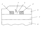
- the figure shows two waveguide cores 1, 2 which have been deposited on a substrate 4, suitably of silicon, with an intervening buffer layer 5.
- Buffer layer 5, which is preferably of silica inhibits the optical fields arising during operation from interacting with substrate 4.
- the cores and the buffer, at least in surrounding regions, are covered with a layer of cladding 6 which may be 20 ⁇ m or more thick, and which plays protective and optical roles.
- the heights of the waveguide cores shown schematically at 1, 2 are 5 ⁇ m it is very difficult to apply a cladding 6 to the region 3 between the waveguide cores.
- the cladding 6 in this region 3 tends to have overhangs and voids, such as that shown schematically at 7, due to significantly less material being deposited.
- a process for applying cladding to closely spaced cores has been developed which reduces the tendency of these undesirable defects to form in the region 3 between the cores.
- firstly the buffer 5 is deposited on the substrate.
- the next stage is to deposit core material by PECVD, and then to selectively etch the deposited core material to leave a pattern of two cores 1, 2 with an intervening volume 3 in the form of a channel of rectangular cross-section.
- the cores are typically 5 ⁇ m deep and about 6 ⁇ m in width with a separation channel between the cores having a width typically in the range from 1 to 8 ⁇ m.
- the amount of cladding 6 material that can be deposited as a final step by PECVD in the region 3 depends upon the range of angles from which material can reach the region. Hence the occurrence of the formation of overhangs and voids, such as that shown schematically at 7, which may be 3 ⁇ m wide, may be minimised.
- this embodiment includes a special cladding process, as the final deposition step, incorporating boron phosphorus silica glass as the composition of the material of cladding 6.
- the cladding includes four stages of deposition and annealing, as follows.
- the cladding composition is silica glass containing 2.4 weight % Phosphorus and 3.4 weight % Boron.
- the composition is suitable for the deposition, and also has a lower flowing temperature than the cores 1, 2 and has a refractive index close to that of the pure silica buffer 5.
- Optical performance has improved performance in comparison with previously produced cladding.
Landscapes
- Physics & Mathematics (AREA)
- Engineering & Computer Science (AREA)
- Microelectronics & Electronic Packaging (AREA)
- General Physics & Mathematics (AREA)
- Optics & Photonics (AREA)
- Optical Integrated Circuits (AREA)
Claims (3)
- Verfahren zur Herstellung einer ummantelten Wellenleiterpaar-Baugruppe durch eine plasmaverstärkte chemische Dampfabscheidung (PECVD), das die Abscheidung einer Pufferschicht (5) aus dielektrischem Material auf einem Substrat (4), die Abscheidung eines Paares von mit Abstand voneinander angeordneten dielektrischen Wellenleiterkernen (1, 2) auf der Pufferschicht, wobei die Kerne aus einem Material mit einem höheren Brechungsindex als der Brechungsindex der Pufferschicht bestehen, und die Erzeugung einer Schicht (6) der Ummantelung über dem Paar von Kernen und dem angrenzenden Bereich der Pufferschicht unter Einschluß des Zwischenraumes (3) zwischen den Kernen des Paares umfaßt, wobei das Material der Ummantelungsschicht (6) einen niedrigeren Brechungsindex als das Material der Kerne und eine niedrigere Fließtemperatur als die der Materialien der Kerne und des Puffers aufweist, wobei die Ummantelungsschicht (6) in mehreren Stufen hergestellt wird und jede Stufe einen PECVD-Abscheidungsschritt gefolgt durch einen Wärmebehandlungsschritt einschließt, bei dem das abgeschiedene Material zum Fließen gebracht wird.
- Verfahren nach Anspruch 1, bei dem der Abscheidungsschritt jeder Abscheidungsstufe bei der Herstellung der Ummantelungsschicht (6) die PECVD-Abscheidung von BPSG-Quarzglas umfaßt, das aus 2,4 Gewichtsprozenten Phosphor und 3,4 Gewichtsprozenten Bor besteht.
- Verfahren nach Anspruch 1 oder 2, bei dem der Wärmebehandlungsschritt jeder Abscheidungsstufe in der Herstellung der Ummantelungsschicht (6) das Fließen bei 1000°C über eine Stunde einschließt.
Applications Claiming Priority (3)
| Application Number | Priority Date | Filing Date | Title |
|---|---|---|---|
| GB9600345 | 1996-01-09 | ||
| GB9600345A GB2309096A (en) | 1996-01-09 | 1996-01-09 | Optical waveguide pair with cladding on buffered substrate |
| PCT/GB1997/000040 WO1997025636A1 (en) | 1996-01-09 | 1997-01-08 | Waveguide pair with cladding |
Publications (2)
| Publication Number | Publication Date |
|---|---|
| EP0873531A1 EP0873531A1 (de) | 1998-10-28 |
| EP0873531B1 true EP0873531B1 (de) | 2000-06-14 |
Family
ID=10786753
Family Applications (1)
| Application Number | Title | Priority Date | Filing Date |
|---|---|---|---|
| EP97900292A Expired - Lifetime EP0873531B1 (de) | 1996-01-09 | 1997-01-08 | Verfahren zur herstellung einer wellenleiterpaar mit optischem mantel |
Country Status (7)
| Country | Link |
|---|---|
| US (1) | US6044192A (de) |
| EP (1) | EP0873531B1 (de) |
| JP (1) | JP2000503135A (de) |
| CA (1) | CA2239118A1 (de) |
| DE (1) | DE69702299T2 (de) |
| GB (1) | GB2309096A (de) |
| WO (1) | WO1997025636A1 (de) |
Families Citing this family (25)
| Publication number | Priority date | Publication date | Assignee | Title |
|---|---|---|---|---|
| US5930439A (en) * | 1997-10-01 | 1999-07-27 | Northern Telecom Limited | Planar optical waveguide |
| US6775453B1 (en) * | 1998-12-21 | 2004-08-10 | Lsi Logic Corporation | On-chip graded index of refraction optical waveguide and damascene method of fabricating the same |
| US6803222B2 (en) * | 2000-11-22 | 2004-10-12 | Kao Corporation | Alkaline proteases |
| US6887514B2 (en) | 2001-05-31 | 2005-05-03 | Dalsa Semiconductor Inc. | Method of depositing optical films |
| US6553170B2 (en) * | 2001-08-31 | 2003-04-22 | Lightwave Microsystems Corporation | Method and system for a combination of high boron and low boron BPSG top clad fabrication process for a planar lightwave circuit |
| US6732550B2 (en) * | 2001-09-06 | 2004-05-11 | Lightwave Microsystems, Inc. | Method for performing a deep trench etch for a planar lightwave circuit |
| US20030070451A1 (en) * | 2001-10-11 | 2003-04-17 | Luc Ouellet | Method of reducing stress-induced mechanical problems in optical components |
| JP3770158B2 (ja) | 2001-12-26 | 2006-04-26 | ソニー株式会社 | Mems素子の製造方法 |
| US7343071B2 (en) * | 2002-06-04 | 2008-03-11 | Ignis Technologies As | Optical component and a method of fabricating an optical component |
| US6768828B2 (en) | 2002-11-04 | 2004-07-27 | Little Optics Inc. | Integrated optical circuit with dense planarized cladding layer |
| US7062141B2 (en) * | 2002-12-12 | 2006-06-13 | Applied Materials, Inc. | Deposition of thick BPSG layers as upper and lower cladding for optoelectronics applications |
| EP1656573A1 (de) * | 2003-08-19 | 2006-05-17 | Ignis Technologies AS | Spot-grössenumsetzer in integrierter optik und herstellungsverfahren |
| JP3911271B2 (ja) * | 2004-01-27 | 2007-05-09 | Tdk株式会社 | 光導波路及びその製造方法 |
| JP2005249895A (ja) * | 2004-03-02 | 2005-09-15 | Tdk Corp | 石英光導波路及びその製造方法 |
| JP2006119379A (ja) * | 2004-10-21 | 2006-05-11 | Sumitomo Electric Ind Ltd | 光導波路デバイスの製造方法、および光導波路デバイス |
| US7712333B2 (en) * | 2006-03-29 | 2010-05-11 | Asahi Glass Company, Limited | Method for smoothing a surface of a glass substrate for a reflective mask blank used in EUV lithography |
| US8045834B2 (en) * | 2008-05-19 | 2011-10-25 | California Institute Of Technology | Silica-on-silicon waveguides and related fabrication methods |
| US9293887B2 (en) | 2011-06-17 | 2016-03-22 | California Institute Of Technology | Chip-based laser resonator device for highly coherent laser generation |
| US8917444B2 (en) | 2011-06-17 | 2014-12-23 | California Institute Of Technology | Chip-based frequency comb generator with microwave repetition rate |
| US9087542B1 (en) | 2012-12-10 | 2015-07-21 | Western Digital (Fremont), Llc | Method for providing a structure having reduced voids in a magnetic recording transducer |
| JP6587615B2 (ja) | 2014-01-24 | 2019-10-09 | カリフォルニア インスティチュート オブ テクノロジー | デュアル周波数光源 |
| US9595918B2 (en) | 2014-03-06 | 2017-03-14 | California Institute Of Technology | Stable microwave-frequency source based on cascaded brillouin lasers |
| US9905999B2 (en) | 2015-02-26 | 2018-02-27 | California Institute Of Technology | Optical frequency divider based on an electro-optical-modulator frequency comb |
| US10476967B2 (en) | 2017-11-14 | 2019-11-12 | Ford Global Technologies, Llc | Vehicle cabin mobile device detection system |
| US10469589B2 (en) | 2017-11-14 | 2019-11-05 | Ford Global Technologies, Llc | Vehicle cabin mobile device sensor system |
Citations (1)
| Publication number | Priority date | Publication date | Assignee | Title |
|---|---|---|---|---|
| EP0803589A1 (de) * | 1995-11-09 | 1997-10-29 | Nec Corporation | Verfahren zur Herstellung eines blasenfreien Lichtwellenleiters |
Family Cites Families (17)
| Publication number | Priority date | Publication date | Assignee | Title |
|---|---|---|---|---|
| DE3536780A1 (de) * | 1985-10-16 | 1987-04-16 | Schott Glaswerke | Verfahren zur herstellung eines planaren lichtwellenleiters |
| JPH01152420A (ja) * | 1987-12-09 | 1989-06-14 | Hitachi Ltd | 導波路型光合分波器 |
| JP2585332B2 (ja) * | 1987-12-25 | 1997-02-26 | 株式会社日立製作所 | 導波路型光デバイス |
| FR2626082B1 (fr) * | 1988-01-14 | 1991-10-18 | Commissariat Energie Atomique | Dispositif d'optique integree permettant de separer les composantes polarisees d'un champ electromagnetique guide et procede de realisation du dispositif |
| JP3070018B2 (ja) * | 1991-12-06 | 2000-07-24 | 日本電信電話株式会社 | 石英系光導波路及びその製造方法 |
| JPH05273426A (ja) * | 1991-12-06 | 1993-10-22 | Sumitomo Electric Ind Ltd | 光導波膜の作製方法およびこれを用いた光導波路の作製方法 |
| GB9202463D0 (en) * | 1992-02-05 | 1992-03-18 | British Telecomm | Silica waveguide structure |
| JPH0659147A (ja) * | 1992-08-11 | 1994-03-04 | Hitachi Cable Ltd | 光導波路及びその製造方法 |
| JP2637891B2 (ja) * | 1993-03-26 | 1997-08-06 | 日本電気株式会社 | 光導波路の製造方法 |
| JPH07140336A (ja) * | 1993-09-22 | 1995-06-02 | Shin Etsu Chem Co Ltd | 光導波路 |
| US5467415A (en) * | 1994-04-22 | 1995-11-14 | At&T Corp. | Method for making polarization independent silica optical circuits |
| JPH0854528A (ja) * | 1994-08-10 | 1996-02-27 | Furukawa Electric Co Ltd:The | 光導波路の製造方法 |
| US5483613A (en) * | 1994-08-16 | 1996-01-09 | At&T Corp. | Optical device with substrate and waveguide structure having thermal matching interfaces |
| DE69512688T2 (de) * | 1994-09-23 | 2000-05-04 | British Telecommunications P.L.C., London | Methode zur Herstellung eines planaren Wellenleiters |
| US5749132A (en) * | 1995-08-30 | 1998-05-12 | Ramar Corporation | Method of fabrication an optical waveguide |
| JP2765545B2 (ja) * | 1995-12-26 | 1998-06-18 | 日本電気株式会社 | 光波長弁別回路およびその製造方法 |
| GB2312525A (en) * | 1996-04-24 | 1997-10-29 | Northern Telecom Ltd | Providing cladding on planar optical waveguide by heating to flow |
-
1996
- 1996-01-09 GB GB9600345A patent/GB2309096A/en not_active Withdrawn
-
1997
- 1997-01-08 EP EP97900292A patent/EP0873531B1/de not_active Expired - Lifetime
- 1997-01-08 US US09/091,257 patent/US6044192A/en not_active Expired - Fee Related
- 1997-01-08 WO PCT/GB1997/000040 patent/WO1997025636A1/en not_active Ceased
- 1997-01-08 DE DE69702299T patent/DE69702299T2/de not_active Expired - Fee Related
- 1997-01-08 JP JP9524974A patent/JP2000503135A/ja active Pending
- 1997-01-08 CA CA002239118A patent/CA2239118A1/en not_active Abandoned
Patent Citations (1)
| Publication number | Priority date | Publication date | Assignee | Title |
|---|---|---|---|---|
| EP0803589A1 (de) * | 1995-11-09 | 1997-10-29 | Nec Corporation | Verfahren zur Herstellung eines blasenfreien Lichtwellenleiters |
Also Published As
| Publication number | Publication date |
|---|---|
| DE69702299T2 (de) | 2000-12-21 |
| JP2000503135A (ja) | 2000-03-14 |
| GB2309096A (en) | 1997-07-16 |
| WO1997025636A1 (en) | 1997-07-17 |
| GB9600345D0 (en) | 1996-03-13 |
| EP0873531A1 (de) | 1998-10-28 |
| DE69702299D1 (de) | 2000-07-20 |
| US6044192A (en) | 2000-03-28 |
| CA2239118A1 (en) | 1997-07-17 |
Similar Documents
| Publication | Publication Date | Title |
|---|---|---|
| EP0873531B1 (de) | Verfahren zur herstellung einer wellenleiterpaar mit optischem mantel | |
| CA1323783C (en) | Device including a substrate-supported optical waveguide, and method of manufacture | |
| JP2002236230A (ja) | 平面型光学導波路素子 | |
| US6553170B2 (en) | Method and system for a combination of high boron and low boron BPSG top clad fabrication process for a planar lightwave circuit | |
| CA2352919A1 (en) | Method for making a planar waveguide | |
| US6909831B2 (en) | Optical waveguide | |
| EP0701150B1 (de) | Verfahren zum Herstellen von Braggreflektoren für Wellenleiter und damit erhaltene Produkte | |
| EP0484011A2 (de) | Verpackung von optischen Komponenten aus Silizium | |
| US6705124B2 (en) | High-density plasma deposition process for fabricating a top clad for planar lightwave circuit devices | |
| JPS6291434A (ja) | 平面状光導波路の製造方法 | |
| GB2181861A (en) | Method of making a planar lightwave guide | |
| US20020039474A1 (en) | Birefringence-free passive optical component | |
| US20030041624A1 (en) | Method for performing a deep trench etch for a planar lightwave circuit | |
| US6996320B2 (en) | Using deuterated source gases to fabricate low loss GeSiON and SiON waveguides | |
| US6864512B2 (en) | Optical waveguide with layered core and methods of manufacture thereof | |
| CA2295052A1 (en) | Method of fabricating an optical component and optical component made thereby | |
| US7099548B2 (en) | Reduction of polarization dependence in planar optical waveguides | |
| EP1030413B1 (de) | Planarer optischen Wellenleiterverstärker und dessen Herstellungsverfahren | |
| US7290407B1 (en) | Triangle-shaped planar optical waveguide having reduced scattering loss | |
| Hattori et al. | Inductively Coupled Plasma-Enhanced Chemical Vapor Deposition of SiO2 and GeO2–SiO2 Films for Optical Waveguides Using Tetraethylorthosilicate and Tetramethylgermanium | |
| Sayah et al. | Dielectric waveguides fabricated on InP by photochemical process for OEICs | |
| Hanada et al. | Polarization Independent FDM/WDM Coupler Using Low Birefringence Silica Optical Waveguide Deposited by APCVD | |
| WO2003005084A1 (en) | A photonic signal transmitting device | |
| JPH06265752A (ja) | スターカップラ |
Legal Events
| Date | Code | Title | Description |
|---|---|---|---|
| PUAI | Public reference made under article 153(3) epc to a published international application that has entered the european phase |
Free format text: ORIGINAL CODE: 0009012 |
|
| 17P | Request for examination filed |
Effective date: 19980810 |
|
| AK | Designated contracting states |
Kind code of ref document: A1 Designated state(s): DE FR GB IT |
|
| 17Q | First examination report despatched |
Effective date: 19990316 |
|
| RAP3 | Party data changed (applicant data changed or rights of an application transferred) |
Owner name: NORTEL NETWORKS CORPORATION |
|
| GRAG | Despatch of communication of intention to grant |
Free format text: ORIGINAL CODE: EPIDOS AGRA |
|
| RTI1 | Title (correction) |
Free format text: METHOD OF PRODUCING A CLADDED WAVEGUIDE PAIR ASSEMBLY |
|
| GRAG | Despatch of communication of intention to grant |
Free format text: ORIGINAL CODE: EPIDOS AGRA |
|
| GRAH | Despatch of communication of intention to grant a patent |
Free format text: ORIGINAL CODE: EPIDOS IGRA |
|
| GRAH | Despatch of communication of intention to grant a patent |
Free format text: ORIGINAL CODE: EPIDOS IGRA |
|
| GRAA | (expected) grant |
Free format text: ORIGINAL CODE: 0009210 |
|
| AK | Designated contracting states |
Kind code of ref document: B1 Designated state(s): DE FR GB IT |
|
| REF | Corresponds to: |
Ref document number: 69702299 Country of ref document: DE Date of ref document: 20000720 |
|
| ET | Fr: translation filed | ||
| ITF | It: translation for a ep patent filed | ||
| RAP2 | Party data changed (patent owner data changed or rights of a patent transferred) |
Owner name: NORTEL NETWORKS LIMITED |
|
| PLBE | No opposition filed within time limit |
Free format text: ORIGINAL CODE: 0009261 |
|
| STAA | Information on the status of an ep patent application or granted ep patent |
Free format text: STATUS: NO OPPOSITION FILED WITHIN TIME LIMIT |
|
| 26N | No opposition filed | ||
| REG | Reference to a national code |
Ref country code: GB Ref legal event code: IF02 |
|
| PGFP | Annual fee paid to national office [announced via postgrant information from national office to epo] |
Ref country code: FR Payment date: 20021209 Year of fee payment: 7 |
|
| PGFP | Annual fee paid to national office [announced via postgrant information from national office to epo] |
Ref country code: GB Payment date: 20021212 Year of fee payment: 7 |
|
| PGFP | Annual fee paid to national office [announced via postgrant information from national office to epo] |
Ref country code: DE Payment date: 20021213 Year of fee payment: 7 |
|
| REG | Reference to a national code |
Ref country code: GB Ref legal event code: 732E |
|
| REG | Reference to a national code |
Ref country code: GB Ref legal event code: 732E |
|
| REG | Reference to a national code |
Ref country code: FR Ref legal event code: TP |
|
| PG25 | Lapsed in a contracting state [announced via postgrant information from national office to epo] |
Ref country code: GB Free format text: LAPSE BECAUSE OF NON-PAYMENT OF DUE FEES Effective date: 20040108 |
|
| PG25 | Lapsed in a contracting state [announced via postgrant information from national office to epo] |
Ref country code: DE Free format text: LAPSE BECAUSE OF NON-PAYMENT OF DUE FEES Effective date: 20040803 |
|
| GBPC | Gb: european patent ceased through non-payment of renewal fee |
Effective date: 20040108 |
|
| PG25 | Lapsed in a contracting state [announced via postgrant information from national office to epo] |
Ref country code: FR Free format text: LAPSE BECAUSE OF NON-PAYMENT OF DUE FEES Effective date: 20040930 |
|
| REG | Reference to a national code |
Ref country code: FR Ref legal event code: ST |
|
| PG25 | Lapsed in a contracting state [announced via postgrant information from national office to epo] |
Ref country code: IT Free format text: LAPSE BECAUSE OF NON-PAYMENT OF DUE FEES;WARNING: LAPSES OF ITALIAN PATENTS WITH EFFECTIVE DATE BEFORE 2007 MAY HAVE OCCURRED AT ANY TIME BEFORE 2007. THE CORRECT EFFECTIVE DATE MAY BE DIFFERENT FROM THE ONE RECORDED. Effective date: 20050108 |