EP0874065A1 - Verbessertes Magnetentwurf für eine Zerstäubungskammer - Google Patents
Verbessertes Magnetentwurf für eine Zerstäubungskammer Download PDFInfo
- Publication number
- EP0874065A1 EP0874065A1 EP98303139A EP98303139A EP0874065A1 EP 0874065 A1 EP0874065 A1 EP 0874065A1 EP 98303139 A EP98303139 A EP 98303139A EP 98303139 A EP98303139 A EP 98303139A EP 0874065 A1 EP0874065 A1 EP 0874065A1
- Authority
- EP
- European Patent Office
- Prior art keywords
- target
- sputtering
- erosion
- magnet
- shape
- Prior art date
- Legal status (The legal status is an assumption and is not a legal conclusion. Google has not performed a legal analysis and makes no representation as to the accuracy of the status listed.)
- Withdrawn
Links
Images




Classifications
-
- H—ELECTRICITY
- H01—ELECTRIC ELEMENTS
- H01J—ELECTRIC DISCHARGE TUBES OR DISCHARGE LAMPS
- H01J37/00—Discharge tubes with provision for introducing objects or material to be exposed to the discharge, e.g. for the purpose of examination or processing thereof
- H01J37/32—Gas-filled discharge tubes
- H01J37/32009—Arrangements for generation of plasma specially adapted for examination or treatment of objects, e.g. plasma sources
- H01J37/32082—Radio frequency generated discharge
- H01J37/321—Radio frequency generated discharge the radio frequency energy being inductively coupled to the plasma
-
- C—CHEMISTRY; METALLURGY
- C23—COATING METALLIC MATERIAL; COATING MATERIAL WITH METALLIC MATERIAL; CHEMICAL SURFACE TREATMENT; DIFFUSION TREATMENT OF METALLIC MATERIAL; COATING BY VACUUM EVAPORATION, BY SPUTTERING, BY ION IMPLANTATION OR BY CHEMICAL VAPOUR DEPOSITION, IN GENERAL; INHIBITING CORROSION OF METALLIC MATERIAL OR INCRUSTATION IN GENERAL
- C23C—COATING METALLIC MATERIAL; COATING MATERIAL WITH METALLIC MATERIAL; SURFACE TREATMENT OF METALLIC MATERIAL BY DIFFUSION INTO THE SURFACE, BY CHEMICAL CONVERSION OR SUBSTITUTION; COATING BY VACUUM EVAPORATION, BY SPUTTERING, BY ION IMPLANTATION OR BY CHEMICAL VAPOUR DEPOSITION, IN GENERAL
- C23C14/00—Coating by vacuum evaporation, by sputtering or by ion implantation of the coating forming material
- C23C14/22—Coating by vacuum evaporation, by sputtering or by ion implantation of the coating forming material characterised by the process of coating
- C23C14/34—Sputtering
- C23C14/35—Sputtering by application of a magnetic field, e.g. magnetron sputtering
-
- H—ELECTRICITY
- H01—ELECTRIC ELEMENTS
- H01J—ELECTRIC DISCHARGE TUBES OR DISCHARGE LAMPS
- H01J37/00—Discharge tubes with provision for introducing objects or material to be exposed to the discharge, e.g. for the purpose of examination or processing thereof
- H01J37/32—Gas-filled discharge tubes
- H01J37/32009—Arrangements for generation of plasma specially adapted for examination or treatment of objects, e.g. plasma sources
- H01J37/32082—Radio frequency generated discharge
- H01J37/321—Radio frequency generated discharge the radio frequency energy being inductively coupled to the plasma
- H01J37/3211—Antennas, e.g. particular shapes of coils
-
- H—ELECTRICITY
- H01—ELECTRIC ELEMENTS
- H01J—ELECTRIC DISCHARGE TUBES OR DISCHARGE LAMPS
- H01J37/00—Discharge tubes with provision for introducing objects or material to be exposed to the discharge, e.g. for the purpose of examination or processing thereof
- H01J37/32—Gas-filled discharge tubes
- H01J37/34—Gas-filled discharge tubes operating with cathodic sputtering
- H01J37/3402—Gas-filled discharge tubes operating with cathodic sputtering using supplementary magnetic fields
- H01J37/3405—Magnetron sputtering
- H01J37/3408—Planar magnetron sputtering
-
- H—ELECTRICITY
- H01—ELECTRIC ELEMENTS
- H01J—ELECTRIC DISCHARGE TUBES OR DISCHARGE LAMPS
- H01J37/00—Discharge tubes with provision for introducing objects or material to be exposed to the discharge, e.g. for the purpose of examination or processing thereof
- H01J37/32—Gas-filled discharge tubes
- H01J37/34—Gas-filled discharge tubes operating with cathodic sputtering
- H01J37/3411—Constructional aspects of the reactor
- H01J37/345—Magnet arrangements in particular for cathodic sputtering apparatus
- H01J37/3452—Magnet distribution
Definitions
- This invention relates to an improved magnet for a plasma physical vapor deposition (hereinafter PVD) chamber.
- PVD plasma physical vapor deposition
- PVD chambers include a target of the material to be sputtered, which target is connected to a source of power, a gas inlet for an inert gas such as argon and other gases, such as nitrogen, if required, and a substrate support mounted parallel to and spaced from the target, which is biased.
- an inert gas such as argon and other gases, such as nitrogen, if required
- substrate support mounted parallel to and spaced from the target, which is biased.
- argon atoms become energized and strike the target, sputtering off atoms of the target material which then deposit on the substrate.
- a magnet pair is mounted above the target on the outside of the chamber. The magnet pair increases the momentum at which argon atoms strike the target.
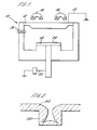
- FIG. 1 is a schematic cross sectional view of a typical sputtering chamber.
- a vacuum chamber 10 includes a target 12 of the material to be sputtered, and a substrate support 14.
- a source of DC power 13 is connected to the target 12.
- a pair of opposed magnets 16, 18 are mounted above the target 12.
- a power source 20, such as a source of RF power is connected to the substrate support 14.
- a substrate 22 is mounted on the substrate support 14.
- a gas inlet 19 permits gases to be passed into the chamber.
- Argon is generally used as the sputtering gas. It is ionized in the chamber and is attracted to the target 12 by the negative potential of the target 12. The argon ions strike the surface of the target and sputter off particles of target material which deposit on the substrate 22.
- collimators In an attempt to improve the directionality of the sputtered particles, collimators have been tried, but they have been unable to greatly improve filling of small diameter, high aspect ratio openings.
- FIG. 3 is a schematic cross sectional view of this improved sputtering chamber, designated as an "ionized metal plasma" or "IMP" chamber.
- the IMP chamber 170 includes a conventional target 172 mounted on a top wall 173 of the chamber 170.
- a pair of opposing magnets 176, 178, are mounted over the top of the chamber 173.
- a substrate support 174 bearing a substrate 175 thereon, is mounted parallel to and spaced from the target 172.
- a source of power 180 is connected to the target 172 and a source of RF power 182 is connected to the substrate support 174.
- a controller 200 regulates gas flows.
- a helical coil 185 is mounted inside the chamber 170 between the target 172 and the substrate support 174, and is connected to a source of RF power 188. Gases in vessels 192, 194 are metered to the chamber by means of flow valves 196, 198.
- the pressure in the chamber is maintained by a cryogenic pump 190 through an inlet 191 via a three position gate valve 199.
- the internal inductively coupled coil 186 provides a high density plasma in the region between the sputtering cathode or target 172 and the substrate support 174.
- sputtered target atoms become ionized and positively charged as they pass through the high density plasma region. They are attracted by the negatively biased substrate and thus impact the substrate in a more vertical direction than occurs in conventional PVD chambers.
- Conventional PVD chambers as shown in Fig. 1 are generally operated at low pressures of about 1-5 millitorr. Under the higher pressures in the IMP chamber, re-sputtering of target material onto the target occurs more frequently. Material that is sputtered from the target in an IMP chamber at higher pressures has a higher possibility to collide with argon molecules, changing the original direction of the sputtered particles. If such a collision occurs close to the target surface, it can be re-directed back towards the target where it re-deposits. Thus the problems of erosion and re-deposition are more severe in the IMP chamber than in conventional PVD chambers. These re-deposited particles are less adherent to the target, and they can flake off as particles, which is always undesirable.
- Improved magnet designs have been developed that provide a more uniform target erosion pattern during sputtering, thereby avoiding or reducing re-deposition at the target surface.
- the erosion track of a target is monitored from the centerline of the target to the edge, and uniformity data used to provide a magnet shape that provides more uniform erosion of the target, particularly for the IMP sputtering chamber.
- Fig. 1 is a schematic cross sectional view of a conventional sputtering chamber.
- Fig. 2 is a schematic cross sectional view of a partially sputter filled opening in accordance with the prior art.
- Fig. 3 is a schematic cross sectional view of a modified sputtering chamber that provides a high density plasma in the chamber.
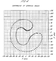
- Fig. 4 depicts the centerline of the erosion track for a magnet of the invention.
- Fig. 5 depicts the centerline of the erosion track for a magnet of the prior art.
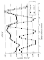
- Fig. 6 is a comparison of the measured erosion track for a target magnet of the invention and a conventional prior art target magnet.
- Fig. 7 is a graph of the erosion profile versus the target radius using a magnet of the invention.
- Fig. 8 is another graph of the erosion profile for another embodiment of a magnet of the invention.
- Fig. 9 illustrates the measured erosion profile for the magnet of Fig. 8.
- Fig. 10 is a top view of the inner and outer pole pieces for a magnet of the invention.
- the target In order to avoid re-deposition of particles on the surface of a target during sputtering, the target ideally erodes uniformly across the target surface. In order to obtain uniform erosion, so that during sputtering the target surface remains as smooth and flat as possible, the shape of the magnet pair above the target must be chosen to provide erosion that is as uniform as possible.
- Fig. 4 shows the data points where the measured B-field of one magnet of the invention is parallel to the target surface and is stronger than 100 Gauss. This corresponds to the centerline of the erosion track of the magnet.
- This erosion track shows a curved, single turn, open ended magnet shape. The ends of the magnet are much wider, by about two times, than the middle portion of the magnet.
- Fig. 5 shows the same data points for a magnet of the prior art.
- This erosion track shows a curved but multi-turn magnet shape, the magnet having about the same width throughout its length.
- Fig. 6 shows the erosion profile of the relative erosion versus the target radius in inches using a conventional magnet (circles) and a magnet of the invention (squares) after 100 hours of burn-in in an IMP chamber wherein the target and the substrate were separated by 135 mm.
- the test was run at 40 millitorr pressure, using 5 kW of power to the target. Thus 500 kW hours of power was applied to the target after 100 hours.
- the magnet shape of Fig. 4 has erosion peaks and valleys that show a more uniform erosion pattern than that of Fig. 5. and it also shows target erosion, with some variation in uniformity, across the whole surface of the target, unlike the magnet shape of Fig. 5. Some variation of the peaks and valleys is needed however to permit re-sputtering of re-deposited material.
- Fig. 7 is a graph of the normalized measured target erosion versus the target radius.
- the dotted vertical line marked “V” shows the position of the helical coil in the chamber.
- the helical coil which was floating, obviously caused some anomalies during sputtering, e.g., a distortion in the electric field at the target which caused reduced erosion of the target at the corresponding target radius.
- Fig. 8 is a graph of the centerline for another magnet of the invention. This magnet shape also has a curved, single turn shape, but the width near the open ends are wider than the magnet of Fig. 4 and it is larger overall.
- Fig. 9 is an erosion profile of the relative erosion versus the target radius using the magnet of Fig. 8 after a burn-in at 38 millitorr pressure, using 3.5 Watts of DC power, and 3 kW of RF power after 430 hours of operation.
- the original target surface is shown at "A”.
- the target erosion was measured as a function of the target radius from the center. It is apparent that the erosion is quite uniform. The deepest erosion was about one-half way between the centerline and the edge of the target, and was only 37 mils deep.
- Fig. 10 is a top view of the pole pieces for the magnet pair of Fig. 8. There are inner pole pieces and an outer pole piece, the inner pole pieces being entirely surrounded by the outer pole piece and they are located within the arc of the outer pole piece.
Landscapes
- Chemical & Material Sciences (AREA)
- Engineering & Computer Science (AREA)
- Physics & Mathematics (AREA)
- Analytical Chemistry (AREA)
- Plasma & Fusion (AREA)
- Materials Engineering (AREA)
- Organic Chemistry (AREA)
- Metallurgy (AREA)
- Mechanical Engineering (AREA)
- Chemical Kinetics & Catalysis (AREA)
- Physical Vapour Deposition (AREA)
- Electrodes Of Semiconductors (AREA)
- Physical Deposition Of Substances That Are Components Of Semiconductor Devices (AREA)
Applications Claiming Priority (2)
| Application Number | Priority Date | Filing Date | Title |
|---|---|---|---|
| US842130 | 1997-04-23 | ||
| US08/842,130 US5876574A (en) | 1997-04-23 | 1997-04-23 | Magnet design for a sputtering chamber |
Publications (1)
| Publication Number | Publication Date |
|---|---|
| EP0874065A1 true EP0874065A1 (de) | 1998-10-28 |
Family
ID=25286595
Family Applications (1)
| Application Number | Title | Priority Date | Filing Date |
|---|---|---|---|
| EP98303139A Withdrawn EP0874065A1 (de) | 1997-04-23 | 1998-04-23 | Verbessertes Magnetentwurf für eine Zerstäubungskammer |
Country Status (6)
| Country | Link |
|---|---|
| US (1) | US5876574A (de) |
| EP (1) | EP0874065A1 (de) |
| JP (1) | JPH1129865A (de) |
| KR (1) | KR19980081599A (de) |
| SG (1) | SG68045A1 (de) |
| TW (1) | TW442851B (de) |
Cited By (4)
| Publication number | Priority date | Publication date | Assignee | Title |
|---|---|---|---|---|
| US6165567A (en) * | 1999-04-12 | 2000-12-26 | Motorola, Inc. | Process of forming a semiconductor device |
| WO2006074013A1 (en) * | 2005-01-05 | 2006-07-13 | Applied Materials, Inc. | Multi-track magnetron exhibiting more uniform deposition and reduced rotational asymmetry |
| CN102789941A (zh) * | 2011-05-18 | 2012-11-21 | 北京北方微电子基地设备工艺研究中心有限责任公司 | 一种磁控管、磁控管的制造方法及物理沉积室 |
| WO2023080937A1 (en) * | 2021-11-05 | 2023-05-11 | Applied Materials, Inc. | Etch uniformity improvement for single turn internal coil pvd chamber |
Families Citing this family (24)
| Publication number | Priority date | Publication date | Assignee | Title |
|---|---|---|---|---|
| US6080669A (en) * | 1999-01-05 | 2000-06-27 | Advanced Micro Devices, Inc. | Semiconductor interconnect interface processing by high pressure deposition |
| US6143140A (en) * | 1999-08-16 | 2000-11-07 | Applied Materials, Inc. | Method and apparatus to improve the side wall and bottom coverage in IMP process by using magnetic field |
| US6627056B2 (en) * | 2000-02-16 | 2003-09-30 | Applied Materials, Inc. | Method and apparatus for ionized plasma deposition |
| TW512180B (en) * | 2000-09-21 | 2002-12-01 | Promos Technologies Inc | Method for maintaining the cleanness of a vacuum chamber of physical vapor deposition system |
| US6699372B2 (en) | 2001-04-16 | 2004-03-02 | Agere Systems Guardian Corporation | Method of coil preparation for ionized metal plasma process and method of manufacturing integrated circuits |
| US7513982B2 (en) * | 2004-01-07 | 2009-04-07 | Applied Materials, Inc. | Two dimensional magnetron scanning for flat panel sputtering |
| US8500975B2 (en) * | 2004-01-07 | 2013-08-06 | Applied Materials, Inc. | Method and apparatus for sputtering onto large flat panels |
| US20060049040A1 (en) * | 2004-01-07 | 2006-03-09 | Applied Materials, Inc. | Apparatus and method for two dimensional magnetron scanning for sputtering onto flat panels |
| US20050245167A1 (en) * | 2004-04-28 | 2005-11-03 | Diana Sinisi | Building toy set |
| JP4923450B2 (ja) * | 2005-07-01 | 2012-04-25 | 富士ゼロックス株式会社 | バッチ処理支援装置および方法、プログラム |
| US20070084720A1 (en) * | 2005-07-13 | 2007-04-19 | Akihiro Hosokawa | Magnetron sputtering system for large-area substrates having removable anodes |
| US20070012559A1 (en) * | 2005-07-13 | 2007-01-18 | Applied Materials, Inc. | Method of improving magnetron sputtering of large-area substrates using a removable anode |
| US20070012558A1 (en) * | 2005-07-13 | 2007-01-18 | Applied Materials, Inc. | Magnetron sputtering system for large-area substrates |
| US20070012663A1 (en) * | 2005-07-13 | 2007-01-18 | Akihiro Hosokawa | Magnetron sputtering system for large-area substrates having removable anodes |
| US20070051616A1 (en) * | 2005-09-07 | 2007-03-08 | Le Hienminh H | Multizone magnetron assembly |
| US7588668B2 (en) | 2005-09-13 | 2009-09-15 | Applied Materials, Inc. | Thermally conductive dielectric bonding of sputtering targets using diamond powder filler or thermally conductive ceramic fillers |
| US20070056850A1 (en) * | 2005-09-13 | 2007-03-15 | Applied Materials, Inc. | Large-area magnetron sputtering chamber with individually controlled sputtering zones |
| US20070056843A1 (en) * | 2005-09-13 | 2007-03-15 | Applied Materials, Inc. | Method of processing a substrate using a large-area magnetron sputtering chamber with individually controlled sputtering zones |
| KR100910673B1 (ko) * | 2006-08-04 | 2009-08-04 | 어플라이드 머티어리얼스, 인코포레이티드 | 다중 마그네트론들, 특히 2 레벨 접지형 마그네트론들의집단 스캐닝 |
| US8961756B2 (en) * | 2006-08-04 | 2015-02-24 | Applied Materials, Inc. | Ganged scanning of multiple magnetrons, especially two level folded magnetrons |
| US20110108068A1 (en) * | 2007-05-25 | 2011-05-12 | Ecolab Usa Inc. | Enhanced melting point rinse aid solids |
| CN102737928B (zh) * | 2011-04-02 | 2014-12-17 | 北京北方微电子基地设备工艺研究中心有限责任公司 | 磁极组件及具有它的磁控管、溅射室装置和基片处理设备 |
| CN103177916B (zh) * | 2011-12-20 | 2015-09-02 | 北京北方微电子基地设备工艺研究中心有限责任公司 | 一种磁控管及磁控溅射设备 |
| CN103887130B (zh) * | 2012-12-21 | 2016-08-31 | 北京北方微电子基地设备工艺研究中心有限责任公司 | 磁控管以及应用该磁控管的磁控溅射设备 |
Citations (3)
| Publication number | Priority date | Publication date | Assignee | Title |
|---|---|---|---|---|
| EP0439361A2 (de) * | 1990-01-26 | 1991-07-31 | Varian Associates, Inc. | Ferstaubungsanlage mit rotierender Magnetanordnung, deren Geometrie ein vorgegebenes Targetabtragsprofil erzeugt |
| EP0451642A2 (de) * | 1990-03-30 | 1991-10-16 | Applied Materials, Inc. | Zerstäubungssystem |
| DE4039101A1 (de) * | 1990-12-07 | 1992-06-11 | Leybold Ag | Ortsfeste magnetron-zerstaeubungskathode fuer vakuumbeschichtungsanlagen |
Family Cites Families (16)
| Publication number | Priority date | Publication date | Assignee | Title |
|---|---|---|---|---|
| JPS6260866A (ja) * | 1985-08-02 | 1987-03-17 | Fujitsu Ltd | マグネトロンスパツタ装置 |
| JP2602276B2 (ja) * | 1987-06-30 | 1997-04-23 | 株式会社日立製作所 | スパツタリング方法とその装置 |
| JPH01279752A (ja) * | 1988-04-30 | 1989-11-10 | Nec Home Electron Ltd | スパッタリング方法及びその装置 |
| JP2627651B2 (ja) * | 1988-10-17 | 1997-07-09 | アネルバ株式会社 | マグネトロンスパッタリング装置 |
| JPH02298266A (ja) * | 1989-05-11 | 1990-12-10 | Fujitsu Ltd | マグネトロンスパッタリング装置 |
| US4995958A (en) * | 1989-05-22 | 1991-02-26 | Varian Associates, Inc. | Sputtering apparatus with a rotating magnet array having a geometry for specified target erosion profile |
| US5252194A (en) * | 1990-01-26 | 1993-10-12 | Varian Associates, Inc. | Rotating sputtering apparatus for selected erosion |
| US5320728A (en) * | 1990-03-30 | 1994-06-14 | Applied Materials, Inc. | Planar magnetron sputtering source producing improved coating thickness uniformity, step coverage and step coverage uniformity |
| US5242566A (en) * | 1990-04-23 | 1993-09-07 | Applied Materials, Inc. | Planar magnetron sputtering source enabling a controlled sputtering profile out to the target perimeter |
| US5178739A (en) * | 1990-10-31 | 1993-01-12 | International Business Machines Corporation | Apparatus for depositing material into high aspect ratio holes |
| JPH0530157U (ja) * | 1991-09-27 | 1993-04-20 | 株式会社島津製作所 | マグネトロンスパツタリング装置 |
| JP2702843B2 (ja) * | 1992-03-19 | 1998-01-26 | 株式会社芝浦製作所 | プレーナ型マグネトロンスパッタリング装置 |
| US5314597A (en) * | 1992-03-20 | 1994-05-24 | Varian Associates, Inc. | Sputtering apparatus with a magnet array having a geometry for a specified target erosion profile |
| JPH05339726A (ja) * | 1992-06-11 | 1993-12-21 | Matsushita Electric Ind Co Ltd | マグネトロンスパッタ装置 |
| US5248402A (en) * | 1992-07-29 | 1993-09-28 | Cvc Products, Inc. | Apple-shaped magnetron for sputtering system |
| JPH06240453A (ja) * | 1993-02-19 | 1994-08-30 | Ulvac Japan Ltd | マグネトロンスパッタ装置 |
-
1997
- 1997-04-23 US US08/842,130 patent/US5876574A/en not_active Expired - Lifetime
-
1998
- 1998-03-23 SG SG1998000847A patent/SG68045A1/en unknown
- 1998-04-22 TW TW087106188A patent/TW442851B/zh not_active IP Right Cessation
- 1998-04-22 KR KR1019980014294A patent/KR19980081599A/ko not_active Withdrawn
- 1998-04-23 JP JP10113226A patent/JPH1129865A/ja active Pending
- 1998-04-23 EP EP98303139A patent/EP0874065A1/de not_active Withdrawn
Patent Citations (3)
| Publication number | Priority date | Publication date | Assignee | Title |
|---|---|---|---|---|
| EP0439361A2 (de) * | 1990-01-26 | 1991-07-31 | Varian Associates, Inc. | Ferstaubungsanlage mit rotierender Magnetanordnung, deren Geometrie ein vorgegebenes Targetabtragsprofil erzeugt |
| EP0451642A2 (de) * | 1990-03-30 | 1991-10-16 | Applied Materials, Inc. | Zerstäubungssystem |
| DE4039101A1 (de) * | 1990-12-07 | 1992-06-11 | Leybold Ag | Ortsfeste magnetron-zerstaeubungskathode fuer vakuumbeschichtungsanlagen |
Non-Patent Citations (1)
| Title |
|---|
| ONUKI J ET AL: "STUDY ON STEP COVERAGE AND (111) PREFERRED ORIENTATION OF ALUMINUM FILM DEPOSITED BY A NEW SWITCHING BIAS SPUTTERING METHOD", APPLIED PHYSICS LETTERS, vol. 53, no. 11, 12 September 1988 (1988-09-12), pages 968 - 970, XP000052928 * |
Cited By (7)
| Publication number | Priority date | Publication date | Assignee | Title |
|---|---|---|---|---|
| US6165567A (en) * | 1999-04-12 | 2000-12-26 | Motorola, Inc. | Process of forming a semiconductor device |
| WO2006074013A1 (en) * | 2005-01-05 | 2006-07-13 | Applied Materials, Inc. | Multi-track magnetron exhibiting more uniform deposition and reduced rotational asymmetry |
| US7186319B2 (en) * | 2005-01-05 | 2007-03-06 | Applied Materials, Inc. | Multi-track magnetron exhibiting more uniform deposition and reduced rotational asymmetry |
| KR101292651B1 (ko) * | 2005-01-05 | 2013-08-02 | 어플라이드 머티어리얼스, 인코포레이티드 | 보다 균일한 증착 및 감소된 회전 비대칭을 나타내는멀티-트랙 마그네트론 |
| CN102789941A (zh) * | 2011-05-18 | 2012-11-21 | 北京北方微电子基地设备工艺研究中心有限责任公司 | 一种磁控管、磁控管的制造方法及物理沉积室 |
| CN102789941B (zh) * | 2011-05-18 | 2015-07-08 | 北京北方微电子基地设备工艺研究中心有限责任公司 | 一种磁控管、磁控管的制造方法及物理沉积室 |
| WO2023080937A1 (en) * | 2021-11-05 | 2023-05-11 | Applied Materials, Inc. | Etch uniformity improvement for single turn internal coil pvd chamber |
Also Published As
| Publication number | Publication date |
|---|---|
| US5876574A (en) | 1999-03-02 |
| KR19980081599A (ko) | 1998-11-25 |
| SG68045A1 (en) | 1999-10-19 |
| TW442851B (en) | 2001-06-23 |
| JPH1129865A (ja) | 1999-02-02 |
Similar Documents
| Publication | Publication Date | Title |
|---|---|---|
| US5876574A (en) | Magnet design for a sputtering chamber | |
| US6458252B1 (en) | High target utilization magnetic arrangement for a truncated conical sputtering target | |
| KR100740811B1 (ko) | 이온화된 금속 증착용 고밀도 플라즈마 소스 | |
| CN1324641C (zh) | 用于等离子体溅射的与旋转磁控管结合的磁体阵列 | |
| US6183614B1 (en) | Rotating sputter magnetron assembly | |
| US6790323B2 (en) | Self ionized sputtering using a high density plasma source | |
| US8557094B2 (en) | Sputtering chamber having auxiliary backside magnet to improve etch uniformity and magnetron producing sustained self sputtering of ruthenium and tantalum | |
| US7618521B2 (en) | Split magnet ring on a magnetron sputter chamber | |
| US6491801B1 (en) | Auxiliary vertical magnet outside a nested unbalanced magnetron | |
| US7628899B2 (en) | Apparatus and method of positioning a multizone magnetron assembly | |
| US6497802B2 (en) | Self ionized plasma sputtering | |
| US6495009B1 (en) | Auxiliary in-plane magnet inside a nested unbalanced magnetron | |
| US6432285B1 (en) | Planar magnetron sputtering apparatus | |
| US7686928B2 (en) | Pressure switched dual magnetron | |
| CN100437886C (zh) | 磁控管溅射 | |
| US20070051622A1 (en) | Simultaneous ion milling and sputter deposition | |
| JP3749178B2 (ja) | 切頭円錐形スパッタリングターゲットのためのターゲット利用率の高い磁気構成 | |
| CN101142094A (zh) | 磁控管溅射室上的分离磁体环 | |
| US6179974B1 (en) | Apparatus and methods for sputtering |
Legal Events
| Date | Code | Title | Description |
|---|---|---|---|
| PUAI | Public reference made under article 153(3) epc to a published international application that has entered the european phase |
Free format text: ORIGINAL CODE: 0009012 |
|
| AK | Designated contracting states |
Kind code of ref document: A1 Designated state(s): BE CH DE FR GB IE IT LI NL |
|
| AX | Request for extension of the european patent |
Free format text: AL;LT;LV;MK;RO;SI |
|
| 17P | Request for examination filed |
Effective date: 19990401 |
|
| AKX | Designation fees paid |
Free format text: BE CH DE FR GB IE IT LI NL |
|
| STAA | Information on the status of an ep patent application or granted ep patent |
Free format text: STATUS: THE APPLICATION IS DEEMED TO BE WITHDRAWN |
|
| 18D | Application deemed to be withdrawn |
Effective date: 20021101 |