EP0874216A2 - Optische Sonde, Herstellungsverfahren einer optischen Sonde und Rastersondenmikroskop - Google Patents
Optische Sonde, Herstellungsverfahren einer optischen Sonde und Rastersondenmikroskop Download PDFInfo
- Publication number
- EP0874216A2 EP0874216A2 EP98303130A EP98303130A EP0874216A2 EP 0874216 A2 EP0874216 A2 EP 0874216A2 EP 98303130 A EP98303130 A EP 98303130A EP 98303130 A EP98303130 A EP 98303130A EP 0874216 A2 EP0874216 A2 EP 0874216A2
- Authority
- EP
- European Patent Office
- Prior art keywords
- optical probe
- optical
- thin film
- probe
- dielectric
- Prior art date
- Legal status (The legal status is an assumption and is not a legal conclusion. Google has not performed a legal analysis and makes no representation as to the accuracy of the status listed.)
- Granted
Links
- 239000000523 sample Substances 0.000 title claims abstract description 135
- 230000003287 optical effect Effects 0.000 title claims abstract description 119
- 238000004519 manufacturing process Methods 0.000 title claims description 15
- 239000010408 film Substances 0.000 claims description 36
- 239000010409 thin film Substances 0.000 claims description 23
- VYPSYNLAJGMNEJ-UHFFFAOYSA-N silicon dioxide Inorganic materials O=[Si]=O VYPSYNLAJGMNEJ-UHFFFAOYSA-N 0.000 claims description 21
- 239000000835 fiber Substances 0.000 claims description 20
- 239000013307 optical fiber Substances 0.000 claims description 17
- 239000002184 metal Substances 0.000 claims description 14
- 238000005259 measurement Methods 0.000 claims description 11
- 230000007246 mechanism Effects 0.000 claims description 11
- 230000000694 effects Effects 0.000 claims description 10
- 239000010453 quartz Substances 0.000 claims description 7
- 230000008878 coupling Effects 0.000 claims description 6
- 238000010168 coupling process Methods 0.000 claims description 6
- 238000005859 coupling reaction Methods 0.000 claims description 6
- 238000005530 etching Methods 0.000 claims description 4
- 238000002310 reflectometry Methods 0.000 claims description 4
- 239000007787 solid Substances 0.000 claims description 4
- 238000000151 deposition Methods 0.000 claims description 3
- 238000001312 dry etching Methods 0.000 claims description 3
- 239000003989 dielectric material Substances 0.000 claims 2
- 230000000704 physical effect Effects 0.000 claims 2
- 238000006073 displacement reaction Methods 0.000 claims 1
- MCMNRKCIXSYSNV-UHFFFAOYSA-N Zirconium dioxide Chemical compound O=[Zr]=O MCMNRKCIXSYSNV-UHFFFAOYSA-N 0.000 description 26
- 239000010410 layer Substances 0.000 description 17
- 238000000034 method Methods 0.000 description 16
- 229910001635 magnesium fluoride Inorganic materials 0.000 description 11
- 239000007789 gas Substances 0.000 description 10
- 238000009826 distribution Methods 0.000 description 8
- 230000008569 process Effects 0.000 description 8
- 229910052681 coesite Inorganic materials 0.000 description 7
- 229910052906 cristobalite Inorganic materials 0.000 description 7
- 239000000377 silicon dioxide Substances 0.000 description 7
- 238000001228 spectrum Methods 0.000 description 7
- 229910052682 stishovite Inorganic materials 0.000 description 7
- 229910052905 tridymite Inorganic materials 0.000 description 7
- 239000011521 glass Substances 0.000 description 6
- KZBUYRJDOAKODT-UHFFFAOYSA-N Chlorine Chemical compound ClCl KZBUYRJDOAKODT-UHFFFAOYSA-N 0.000 description 5
- 229920002120 photoresistant polymer Polymers 0.000 description 5
- 230000009466 transformation Effects 0.000 description 5
- 239000000463 material Substances 0.000 description 4
- CLDZYSUDOQXJOU-UHFFFAOYSA-M C5-oxacyanine Chemical compound [I-].O1C2=CC=CC=C2[N+](CC)=C1C=CC=CC=C1N(CC)C2=CC=CC=C2O1 CLDZYSUDOQXJOU-UHFFFAOYSA-M 0.000 description 3
- 230000005540 biological transmission Effects 0.000 description 3
- 230000005284 excitation Effects 0.000 description 3
- 230000006870 function Effects 0.000 description 3
- 238000012360 testing method Methods 0.000 description 3
- 230000036962 time dependent Effects 0.000 description 3
- CSCPPACGZOOCGX-UHFFFAOYSA-N Acetone Chemical compound CC(C)=O CSCPPACGZOOCGX-UHFFFAOYSA-N 0.000 description 2
- GWEVSGVZZGPLCZ-UHFFFAOYSA-N Titan oxide Chemical compound O=[Ti]=O GWEVSGVZZGPLCZ-UHFFFAOYSA-N 0.000 description 2
- 239000000853 adhesive Substances 0.000 description 2
- 230000001070 adhesive effect Effects 0.000 description 2
- 238000011156 evaluation Methods 0.000 description 2
- 239000010419 fine particle Substances 0.000 description 2
- 239000000203 mixture Substances 0.000 description 2
- 238000005498 polishing Methods 0.000 description 2
- 229920003229 poly(methyl methacrylate) Polymers 0.000 description 2
- 239000004926 polymethyl methacrylate Substances 0.000 description 2
- 239000000126 substance Substances 0.000 description 2
- VAGJCLDZLVQVPR-UHFFFAOYSA-N C5-oxacyanine cation Chemical compound O1C2=CC=CC=C2[N+](CC)=C1C=CC=CC=C1N(CC)C2=CC=CC=C2O1 VAGJCLDZLVQVPR-UHFFFAOYSA-N 0.000 description 1
- ZAMOUSCENKQFHK-UHFFFAOYSA-N Chlorine atom Chemical compound [Cl] ZAMOUSCENKQFHK-UHFFFAOYSA-N 0.000 description 1
- 229910020323 ClF3 Inorganic materials 0.000 description 1
- MYMOFIZGZYHOMD-UHFFFAOYSA-N Dioxygen Chemical compound O=O MYMOFIZGZYHOMD-UHFFFAOYSA-N 0.000 description 1
- YCKRFDGAMUMZLT-UHFFFAOYSA-N Fluorine atom Chemical compound [F] YCKRFDGAMUMZLT-UHFFFAOYSA-N 0.000 description 1
- GRYLNZFGIOXLOG-UHFFFAOYSA-N Nitric acid Chemical compound O[N+]([O-])=O GRYLNZFGIOXLOG-UHFFFAOYSA-N 0.000 description 1
- 238000001069 Raman spectroscopy Methods 0.000 description 1
- BLRPTPMANUNPDV-UHFFFAOYSA-N Silane Chemical compound [SiH4] BLRPTPMANUNPDV-UHFFFAOYSA-N 0.000 description 1
- ATJFFYVFTNAWJD-UHFFFAOYSA-N Tin Chemical compound [Sn] ATJFFYVFTNAWJD-UHFFFAOYSA-N 0.000 description 1
- QVGXLLKOCUKJST-UHFFFAOYSA-N atomic oxygen Chemical compound [O] QVGXLLKOCUKJST-UHFFFAOYSA-N 0.000 description 1
- VYXSBFYARXAAKO-WTKGSRSZSA-N chembl402140 Chemical compound Cl.C1=2C=C(C)C(NCC)=CC=2OC2=C\C(=N/CC)C(C)=CC2=C1C1=CC=CC=C1C(=O)OCC VYXSBFYARXAAKO-WTKGSRSZSA-N 0.000 description 1
- 239000000460 chlorine Substances 0.000 description 1
- 229910052801 chlorine Inorganic materials 0.000 description 1
- 238000005253 cladding Methods 0.000 description 1
- 239000011248 coating agent Substances 0.000 description 1
- 238000000576 coating method Methods 0.000 description 1
- 239000012792 core layer Substances 0.000 description 1
- 238000005520 cutting process Methods 0.000 description 1
- 230000007423 decrease Effects 0.000 description 1
- 230000003247 decreasing effect Effects 0.000 description 1
- 229910001882 dioxygen Inorganic materials 0.000 description 1
- 230000005684 electric field Effects 0.000 description 1
- 238000010894 electron beam technology Methods 0.000 description 1
- 238000000295 emission spectrum Methods 0.000 description 1
- 238000002474 experimental method Methods 0.000 description 1
- 230000002349 favourable effect Effects 0.000 description 1
- 229910052731 fluorine Inorganic materials 0.000 description 1
- 239000011737 fluorine Substances 0.000 description 1
- 238000010438 heat treatment Methods 0.000 description 1
- 238000010884 ion-beam technique Methods 0.000 description 1
- 230000004298 light response Effects 0.000 description 1
- 239000011159 matrix material Substances 0.000 description 1
- 238000002844 melting Methods 0.000 description 1
- 230000008018 melting Effects 0.000 description 1
- 238000002156 mixing Methods 0.000 description 1
- 229940074355 nitric acid Drugs 0.000 description 1
- 229910017604 nitric acid Inorganic materials 0.000 description 1
- 239000001301 oxygen Substances 0.000 description 1
- 229910052760 oxygen Inorganic materials 0.000 description 1
- 238000012545 processing Methods 0.000 description 1
- 230000001902 propagating effect Effects 0.000 description 1
- 230000004044 response Effects 0.000 description 1
- 239000004065 semiconductor Substances 0.000 description 1
- 238000004611 spectroscopical analysis Methods 0.000 description 1
- 238000012876 topography Methods 0.000 description 1
- JOHWNGGYGAVMGU-UHFFFAOYSA-N trifluorochlorine Chemical compound FCl(F)F JOHWNGGYGAVMGU-UHFFFAOYSA-N 0.000 description 1
- 230000004304 visual acuity Effects 0.000 description 1
Images


Classifications
-
- G—PHYSICS
- G01—MEASURING; TESTING
- G01Q—SCANNING-PROBE TECHNIQUES OR APPARATUS; APPLICATIONS OF SCANNING-PROBE TECHNIQUES, e.g. SCANNING PROBE MICROSCOPY [SPM]
- G01Q60/00—Particular types of SPM [Scanning Probe Microscopy] or microscopes; Essential components thereof
- G01Q60/18—SNOM [Scanning Near-Field Optical Microscopy] or apparatus therefor, e.g. SNOM probes
- G01Q60/22—Probes, their manufacture, or their related instrumentation, e.g. holders
-
- B—PERFORMING OPERATIONS; TRANSPORTING
- B82—NANOTECHNOLOGY
- B82Y—SPECIFIC USES OR APPLICATIONS OF NANOSTRUCTURES; MEASUREMENT OR ANALYSIS OF NANOSTRUCTURES; MANUFACTURE OR TREATMENT OF NANOSTRUCTURES
- B82Y20/00—Nanooptics, e.g. quantum optics or photonic crystals
-
- B—PERFORMING OPERATIONS; TRANSPORTING
- B82—NANOTECHNOLOGY
- B82Y—SPECIFIC USES OR APPLICATIONS OF NANOSTRUCTURES; MEASUREMENT OR ANALYSIS OF NANOSTRUCTURES; MANUFACTURE OR TREATMENT OF NANOSTRUCTURES
- B82Y35/00—Methods or apparatus for measurement or analysis of nanostructures
-
- G—PHYSICS
- G01—MEASURING; TESTING
- G01B—MEASURING LENGTH, THICKNESS OR SIMILAR LINEAR DIMENSIONS; MEASURING ANGLES; MEASURING AREAS; MEASURING IRREGULARITIES OF SURFACES OR CONTOURS
- G01B9/00—Measuring instruments characterised by the use of optical techniques
- G01B9/04—Measuring microscopes
-
- G—PHYSICS
- G01—MEASURING; TESTING
- G01Q—SCANNING-PROBE TECHNIQUES OR APPARATUS; APPLICATIONS OF SCANNING-PROBE TECHNIQUES, e.g. SCANNING PROBE MICROSCOPY [SPM]
- G01Q70/00—General aspects of SPM probes, their manufacture or their related instrumentation, insofar as they are not specially adapted to a single SPM technique covered by group G01Q60/00
- G01Q70/02—Probe holders
-
- Y—GENERAL TAGGING OF NEW TECHNOLOGICAL DEVELOPMENTS; GENERAL TAGGING OF CROSS-SECTIONAL TECHNOLOGIES SPANNING OVER SEVERAL SECTIONS OF THE IPC; TECHNICAL SUBJECTS COVERED BY FORMER USPC CROSS-REFERENCE ART COLLECTIONS [XRACs] AND DIGESTS
- Y10—TECHNICAL SUBJECTS COVERED BY FORMER USPC
- Y10S—TECHNICAL SUBJECTS COVERED BY FORMER USPC CROSS-REFERENCE ART COLLECTIONS [XRACs] AND DIGESTS
- Y10S977/00—Nanotechnology
- Y10S977/84—Manufacture, treatment, or detection of nanostructure
- Y10S977/849—Manufacture, treatment, or detection of nanostructure with scanning probe
- Y10S977/86—Scanning probe structure
- Y10S977/862—Near-field probe
Definitions
- This invention relates to an optical probe used in a near-field effect microscope for the purpose of observing topography or measuring photo-physical properties of a solid surface in the nano-meter range by optically illuminating or photo-exciting a surface to be measured.
- the invention also relates to a method of manufacturing the optical probe and a scanning probe microscope using this optical probe.
- a metal film is deposited on a glass surface having fine particles thereon. Thereafter the fine particles are removed, thus forming a microscopic aperture.
- a probe manufacturing method is disclosed in US Patent 4917462. In that arrangement, a glass tube is extended by heat until it is fractured so as to coat a metal film over a lateral surface of the glass while forming a tip in the form of a thinned glass tube providing a microscopic aperture.
- US Patent 5272330 discloses a probe manufacturing method in which an optical fibre is extended until it is thermally fractured. Again, this provides a metal-coated lateral surface with a microscopic aperture at the tip portion of the thinned optical fibre.
- a functional probe is disclosed by Lewis et al. in Nature 354, 1991, p. 214.
- light is introduced into a functional probe comprising a glass tube having a probe tip packed with a fluorescent substance.
- the arrangement uses the fluorescent light as a microscopic light source. This method, however, presents problems in that the microscopic light source wavelength is restricted in selection and the light source intensity gradually decreases as the fluorescent light fades.
- the problem in the above microscopic-aperture optical probe lies in that the intensity of the evanescent field at the microscopic aperture is greatly decreased, to as little as 1/1000 to 1/10000, with respect to the intensity of incoming light. This acts to prevent against observations of samples at high S/N or processing/writing at high scanning speeds.
- the optical probe of this invention has a microscopic aperture and is an optical resonator or a part thereof; despite the fact that the conventional optical probe utilising a near-field effect suffers large attenuation in the strength of the evanescent field with respect to the incoming light.
- an optical probe which is characterised by an optical resonator or part thereof formed by an optical probe having a microscopic aperture with an increase in the intensity of the light within the optical probe, so that an evanescent field formed at the microscopic aperture portion is increased as compared to conventional probes.
- an optical resonator constituted by an optical fibre that has a microscopic aperture with a diameter of approximately from 50 nano-meter to 200 nano-meters.
- Light is externally incident onto the fibre so as to strengthen the photoelectric field within the optical fibre to a level higher than in the case of not using an optical resonator.
- a dielectric multilayered film or a metal thin film with a reflectivity of 95% or higher, preferably 99% or higher, is coated over the fibre and then a microscopic aperture is provided.
- the fibre having a length of several cm is worked at one end by optical polishing to a planar accuracy of ⁇ /20 or finer and parallelism of 1° or smaller. It is then coated with a dielectric multilayered film having a reflectivity of 85 - 90%. Laser light is introduced through this surface via an objective lens as an optical coupler. The light confined within the optical fibre is amplified within the resonator while it reciprocates between the dielectric multilayered films or metal films placed on the opposite ends. Thus, an evanescent light with a strong electric field strength can be withdrawn through the microscopic aperture.
- FIG. 1 is a view representing a structure of an optical probe showing a first embodiment of the present invention.
- the optical probe is constituted by an SiO 2 fibre 3 formed by a core layer 2 for propagating light and a cladding layer 1 having a different refractive index therefrom.
- the fibre is formed, at one end face, with a dielectric multilayered film 5 of MgF 2 /ZrO 2 having a microscopic transmission bore 33.
- a coupling lens 19 and a dielectric multilayerd film 10 are provided at the other end face of the fibre compared with film 5.
- the dielectric multilayered film 10 is movable in the directions indicated by the arrows using a resonator length/parallelism adjusting mechanism 11. The resonator can thus be adjusted in its length and parallelism.
- the resonator is enhanced in Q factor by this adjustment.
- the resonator length/parallelism adjusting mechanism 11 is constituted by a piezoelectric element.
- the SiO 2 fibre 3 used can be a single mode fibre, a step index fibre, a graded index fibre, a polarisation plane holding fibre, or the like.
- the coupling lens 19 can be placed between the dielectric multilayered film 10 and the optical fibre, or on the other side of the film 10.
- the coupling lens used can be an objective lens of the typed used for microscopes, or an objective lens used through a refractive index aligning oil, or the like.
- the structure of the optical probe as above can amplify the light introduced into the inside of the optical probe by the optical resonator.
- the evanescent light withdrawn through the tip of the optical probe is intensified. This enables measurement in a short time and high-speed scanning when writing into a memory, or the like.
- FIG. 2 shows the structure of an optical probe according to a second embodiment of the present invention.
- a microscopic projection 9 is provided in place of the microscopic bore 33. This is advantageous for observing a sample surface which has a large roughness.
- the effect and operation of this embodiment is the same as in the first embodiment except that the shape of the tip portion of the optical probe is different.
- FIG. 3 shows the structure of an optical probe according to a third embodiment of the present invention. Since the optical probe uses as its material a quartz rod having a length of approximately 100 ⁇ m and the probe size can be reduced, it is possible to use a probe chip like a cantilever. Also, the dielectric multilayered film can be utilised as a reflecting mirror for optical levers. The effect and operation of this embodiment is the same as in the first embodiment except that the shape of the tip portion of the optical probe is different.
- FIG. 4 shows the structure of an optical probe according to a fourth embodiment of the present invention.
- the optical probe has, at its tip, a plurality of microscopic projections formed of SiO 2 .
- the arrangement is advantageous for observing the movement of excited energy causing between atoms or molecules present at a distance between the projections.
- this embodiment 9 i.e. 3 x 3
- microscopic projections are exemplified, the number of the projections is not limited to this.
- the effect and operation of the embodiment is the same as in the first embodiment except that the shape of a tip portion of the optical probe is different.
- FIGs. 5A, 5B, 5C, 5D, 5E, 5F and 5G show the fabrication process of an optical probe according to the present invention.
- First an SiO 2 optical fibre 3 is placed in a vacuum depositing apparatus.
- the fibre is a single-mode optical fibre having mirror-polished end faces, a length of approximately 20 cm, MgF 2 and ZrO 2 as a thin film material, and Cr as a metal mask material.
- the vacuum is reduced to a pressure of approximately 10 -5 Pa.
- ZrO 2 is evaporated by means of an electron-beam melting method, a resistance heating method, or the like.
- a ZrO 2 layer 6 is deposited to a film thickness of 97.56 nm so that the product of the ZrO 2 refractive index 2.05 and the film thickness becomes 200 nm, that is a quarter of the wavelength of the light source used.
- an oxygen gas is introduced into the vacuum apparatus in order to avoid deviation from a stoichiometric composition.
- MgF 2 is evaporated similarly to the case of ZrO 2 ; to deposit an MgF 2 layer 7 to a film thickness of 144.93 nm so that the product of the MgF 2 refractive index 1.38 and the film thickness becomes 200 nm, that is a quarter of the wavelength of the light source used.
- FIG. 5A shows an optical fibre that is deposited with eleven alternate layers of ZrO 2 layers 6 and MgF 2 layers 7 by repeating the above steps.
- Cr layer 4 is deposited to a film thickness of approximately 1 ⁇ m as a mask for dry-etching the MgF 2 /ZrO 2 layer 5(dielectric multilayered film). Then the fibre is removed from the vacuum apparatus and photoresist 8 is applied by a spin coater or the like to a film thickness of approximately 1 ⁇ m.
- photoresist 8 is applied by a spin coater or the like to a film thickness of approximately 1 ⁇ m.
- TiN, TiW or the like may be used in place of Cr.
- FIG. 5B shows the fibre with the described films.
- a photomask 18, which is patterned with a bore 17 opened by ion-beam to a diameter of 500 nm is used, as shown in FIG. 5C.
- the optical fibre of FIG. 5B, with the photoresist 8 applied, is subject to reduced-projection exposure (1/5) and placed in a vacuum apparatus provided with both a dry etch mechanism and a CVD mechanism.
- FIG. 5D shows the photoresist 8 processed to the pattern of FIG. 5C.
- the Cr layer 4 metal mask layer
- a reactive gas such as Cl 2 ; thus forming a mask for etching the dielectric multilayered film 5(MgF 2 /ZrO 2 layer).
- FIG. 5E shows a bore 33, with a diameter of 100 nm, which is opened by repeating the etchings alternately.
- a fluorine-based gas such as C 2 F 6 or the like or a chlorine-based gas such as Cl 2 or the like or a gas containing both gases such as ClF 3 , or the gas mixture of them is introduced into a vacuum apparatus.
- the arrangement is used to alternately deposit a dielectric thin film with a low refractive index, such as MgF 2 , SiO 2 or the like, and a dielectric thin film with a high refractive index, such as ZrO 2 , TiO 2 , TaO 4 or the like.
- an SiO 2 layer 34 is first deposited in the 100-nm diameter bore by a CVD mechanism using gasses of SiH 4 , oxygen and the like.
- FIG. 5F shows a state that the surface of the optical probe is covered by the SiO 2 layer 34.
- the metal mask is removed using a nitric-acid based stripping solution, to make a microscopic projection as shown in FIG. 5C.
- FIGS. 6A and 6B show a manufacturing process for an optical probe according to a third embodiment of the present invention.
- a quartz rod is employed for an optical probe material.
- a bore is opened through the centre of a stainless-made jig 20.
- Jig 20 is a 30-mm square with a thickness of 100 ⁇ m.
- the quartz rod 21 having a diameter of 20 ⁇ m and a length of 200 ⁇ m is fixed therein with an adhesive (FIG. 6A) and mirror-polished by machine polishing (FIG. 6B).
- the quartz rod 21 thus polished is formed with a dielectric multilayered film (MgF 2 /ZrO 2 layer) and a microscopic transmission bore 33, thereby making a Fabry-Perot resonator type optical probe. If the process of making a microscopic projection 9 is further performed, an optical probe of the third embodiment, shown in FIG 3, is achieved.
- a dielectric multilayered film MgF 2 /ZrO 2 layer
- a microscopic transmission bore 33 thereby making a Fabry-Perot resonator type optical probe.
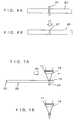
- the optical probe thus made is fixed with an adhesive or the like in a bore portion of a holder 22.
- the holder 22 has a length of several mm, a width of 50 ⁇ m and a height of 50 ⁇ m, as shown in FIG. 7A (front view) and FIG. 7B (side view). Fixing one end 35 of the holder 22 enables utilisation of the probe as a probe chip cantilever. Light from an optical-lever light source is introduced in the direction shown in Fig 7A and a dielectric multilayered film 10, positioned at a terminal end of the optical probe, is utilised as a reflecting mirror. The arrangement thereby functions as an optical lever.
- optical probe of the fourth embodiment of the present invention can be made in a similar process to that of the first and second embodiments. The only difference is the use of a pattern having a 3 X 3 matrix of nine bores formed in the photomask.
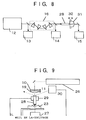
- FIG 8 shows an optical system of a short-pulse optical response characteristic evaluating apparatus used for evaluating the optical probes made according to the described embodiments.
- a titanium-sapphire laser having a basic wavelength of 800 nm and a pulse width of 40 fs is used as a light source.
- the light from the light source 12 was measured as to its pulse width and spectrum width by a (correlator-A/spectroscope-A) 13. It was confirmed that the Fourier transformation limiting pulse was 40 fs and 24 nm.
- This light pulse was passed by a distributed controller 16, constituted by four Brewster prisms, so as to be provided with a negative group velocity distribution.
- the flat convex lens 31 was slightly moved by a coupling-constant varying mechanism 32 using a piezoelectric element so as to adjust the distance from the optical probe.
- the distance between the flat convex lens 31 and the optical probe 28 is 40 nm, the Fourier transformation limiting pulse was obtained. If this distance is increased, the optical coupling through an evanescent light is weakened to increase the positive group velocity distribution. Accordingly, compensation using a prism distribution controller is impossible and the pulse width is broadened without forming a Fourier transformation limiting pulse.
- a distribution controller using a diffraction grating in place of the four Brewster prisms has an equivalent function.
- the test was carried out for an optical fibre probe made according to the second embodiment of the present invention.
- the pulse width and spectrum width measured by (correlator-C/spectroscope-C) 15 gave a minimum value of the pulse width of 41 fs and a maximum value of the spectrum width of 23 nm. These values show a Fourier transformation limiting pulse similarly to the value measured by the (correlator-A/spectroscope-A) 13. Thus showing that a positive distribution due to the optical probe is compensated for by the distribution controller. As a result of various evaluations on this probe, similar effects to the first embodiment were obtained.
- results similar to those with the first and second embodiments were obtained in a short-pulse pass characteristic evaluating experiment for the optical probe of the third embodiment of the present invention. Also, various observations and measurements were carried out by attaching the present optical probe to a scanning probe microscope device similarly to the first and second embodiments. As a result in an emission spectrochemical measurement the emission light intensity was approximately 9 times that of the first embodiment case. The time dependent profile in emission light intensity became long in attenuation time compared with the first embodiment. This shows that the moving process in an excitation state is suppressed by simultaneous excitations at several nearby points.
- FIG 9 shows one example of a structure in which an optical probe according to the present invention is attached to a scanning probe microscope.
- the basic structure is an ATM operating mechanism which detects a force acting between the probe and a sample to control the distance therebetween so that it remains constant.
- An optical probe according to the present invention can be used in place of a cantilever; without changing the apparatus.
- the dielectric multilayered film 10 made at the terminal end of the optical probe can be used as a reflecting mirror. If the light from a light source 26 is introduced into the optical probe, an evanescent field amplified as a resonator can be created to provide favourable S/N measurements.
- the dielectric multilayered film 10 made on the optical probe functions as a wavelength-selecting filter for cutting excitation light so as to transmit fluorescent light.
- a time dependent profile measurement was made as to emission light spectrum and emission light intensity on a sample.
- the sample was made by mixing PMMA with DODCI (3, 3' - diethyl oxadicarbocyanine) which was evaporated and hot compressed.
- DODCI 3, 3' - diethyl oxadicarbocyanine
- An optical probe according to the present invention was tested using 532-nm wavelength light from a Nd:YAG laser. As a result, it was confirmed that the light emission peak wavelength is shifted toward a longer wavelength and shortened in fluorescent life for a high concentration DODCI sample compared with a diluted DODCI sample.
- An optical probe according to the present invention and using a 400-nm wavelength light source was applied in the emission spectrochemical measurement of a solid surface.
- the sample tested was manufactured by dissolving PMMA and rhodamine 6G in acetone to provide a thin-film formed by a spin-coater.
- the light source used was the above-stated titanium-sapphire laser.
- the result of the test was a time dependent measurement profile with clear light emission spectrum and light emission intensity.
Landscapes
- Physics & Mathematics (AREA)
- General Physics & Mathematics (AREA)
- Chemical & Material Sciences (AREA)
- Nuclear Medicine, Radiotherapy & Molecular Imaging (AREA)
- Nanotechnology (AREA)
- Engineering & Computer Science (AREA)
- Health & Medical Sciences (AREA)
- General Health & Medical Sciences (AREA)
- Radiology & Medical Imaging (AREA)
- Crystallography & Structural Chemistry (AREA)
- Analytical Chemistry (AREA)
- Life Sciences & Earth Sciences (AREA)
- Biophysics (AREA)
- Optics & Photonics (AREA)
- Length Measuring Devices By Optical Means (AREA)
Applications Claiming Priority (6)
| Application Number | Priority Date | Filing Date | Title |
|---|---|---|---|
| JP106430/97 | 1997-04-23 | ||
| JP10643097 | 1997-04-23 | ||
| JP10643097 | 1997-04-23 | ||
| JP5116798 | 1998-03-03 | ||
| JP51167/98 | 1998-03-03 | ||
| JP05116798A JP3706868B2 (ja) | 1997-04-23 | 1998-03-03 | 光プローブおよび光プローブ製造方法および走査型プローブ顕微鏡 |
Publications (3)
| Publication Number | Publication Date |
|---|---|
| EP0874216A2 true EP0874216A2 (de) | 1998-10-28 |
| EP0874216A3 EP0874216A3 (de) | 1999-08-04 |
| EP0874216B1 EP0874216B1 (de) | 2004-08-18 |
Family
ID=26391703
Family Applications (1)
| Application Number | Title | Priority Date | Filing Date |
|---|---|---|---|
| EP98303130A Expired - Lifetime EP0874216B1 (de) | 1997-04-23 | 1998-04-23 | Optische Sonde, Herstellungsverfahren einer optischen Sonde und Rastersondenmikroskop |
Country Status (4)
| Country | Link |
|---|---|
| US (1) | US6121604A (de) |
| EP (1) | EP0874216B1 (de) |
| JP (1) | JP3706868B2 (de) |
| DE (1) | DE69825657T2 (de) |
Families Citing this family (14)
| Publication number | Priority date | Publication date | Assignee | Title |
|---|---|---|---|---|
| JP3535356B2 (ja) * | 1997-09-18 | 2004-06-07 | 片岡 俊彦 | 光共振器を利用した走査型近接場光学顕微鏡 |
| JP3559453B2 (ja) * | 1998-06-29 | 2004-09-02 | 株式会社東芝 | 発光素子 |
| US6835963B2 (en) * | 1999-12-22 | 2004-12-28 | Kabushiki Kaisha Toshiba | Light-emitting element and method of fabrication thereof |
| US6642517B1 (en) * | 2000-01-25 | 2003-11-04 | Veeco Instruments, Inc. | Method and apparatus for atomic force microscopy |
| US6913713B2 (en) * | 2002-01-25 | 2005-07-05 | Konarka Technologies, Inc. | Photovoltaic fibers |
| US20040091064A1 (en) * | 2002-11-12 | 2004-05-13 | Broadcom Corporation | Phase detector with delay elements for improved data regeneration |
| US20050153064A1 (en) * | 2004-01-14 | 2005-07-14 | Asml Holding N.V. | Method of covering clear aperture of optic during deposition of glue protection layer |
| JP5033609B2 (ja) * | 2007-03-12 | 2012-09-26 | 株式会社日立製作所 | 走査プローブ顕微鏡およびこれを用いた試料の観察方法 |
| JP4929106B2 (ja) * | 2007-09-06 | 2012-05-09 | 日本分光株式会社 | 近接場ファイバープローブ、及び近接場光学顕微鏡 |
| JP5216509B2 (ja) | 2008-03-05 | 2013-06-19 | 株式会社日立製作所 | 走査プローブ顕微鏡およびこれを用いた試料の観察方法 |
| US20100097779A1 (en) * | 2008-10-21 | 2010-04-22 | Mitutoyo Corporation | High intensity pulsed light source configurations |
| JP2014066701A (ja) * | 2012-09-04 | 2014-04-17 | Canon Inc | 被検体情報取得装置 |
| JP6692088B2 (ja) * | 2015-08-28 | 2020-05-13 | 国立大学法人金沢大学 | 液中原子間力顕微鏡 |
| CN108645369A (zh) * | 2018-05-16 | 2018-10-12 | 大连大学 | 相对基准要素轴线的平行度基准方向判断方法 |
Family Cites Families (23)
| Publication number | Priority date | Publication date | Assignee | Title |
|---|---|---|---|---|
| US4662747A (en) * | 1983-08-03 | 1987-05-05 | Cornell Research Foundation, Inc. | Method and apparatus for production and use of nanometer scale light beams |
| JPH0711629B2 (ja) * | 1989-09-04 | 1995-02-08 | 新技術事業団 | 光走査トンネル顕微鏡 |
| JP2753590B2 (ja) * | 1989-11-30 | 1998-05-20 | 横河電機株式会社 | 高密度メモリー装置 |
| JP2941911B2 (ja) * | 1990-03-27 | 1999-08-30 | 科学技術振興事業団 | 反射型光走査トンネル顕微鏡 |
| US5168538A (en) * | 1991-01-16 | 1992-12-01 | Gillespie Donald E | Optical probe employing an impedance matched sub-lambda transmission line |
| JPH05203879A (ja) * | 1992-01-27 | 1993-08-13 | Nikon Corp | 反射共振型近接場走査型顕微鏡 |
| JPH05264905A (ja) * | 1992-03-23 | 1993-10-15 | Nikon Corp | 走査型近接場顕微鏡 |
| JP3267685B2 (ja) * | 1992-07-28 | 2002-03-18 | セイコーインスツルメンツ株式会社 | 微細表面観察装置 |
| JPH06281414A (ja) * | 1993-03-29 | 1994-10-07 | Olympus Optical Co Ltd | 光集積型変位計測装置 |
| JPH0712826A (ja) * | 1993-06-29 | 1995-01-17 | Hitachi Ltd | 干渉計、光走査型トンネル顕微鏡および光プローブ |
| US5389779A (en) * | 1993-07-29 | 1995-02-14 | At&T Corp. | Method and apparatus for near-field, scanning, optical microscopy by reflective, optical feedback |
| US5395741A (en) * | 1993-12-22 | 1995-03-07 | At&T Corp. | Method of making fiber probe devices using patterned reactive ion etching |
| US5812723A (en) * | 1994-03-24 | 1998-09-22 | Kanagawa Academy Of Science And Technology | Optical fiber with tapered end of core protruding from clad |
| JP3097892B2 (ja) * | 1994-03-25 | 2000-10-10 | 財団法人神奈川科学技術アカデミー | 光ファイバ及びその加工方法、光ファイバプローブ及びその製造方法 |
| JP3023048B2 (ja) * | 1994-03-24 | 2000-03-21 | 財団法人神奈川科学技術アカデミー | 光ファイバプローブ及びその製造方法 |
| DE69535741T2 (de) * | 1994-05-31 | 2009-05-07 | Kanagawa Academy Of Science And Technology, Kawasaki | Optische faser und deren herstellung |
| JPH087323A (ja) * | 1994-06-17 | 1996-01-12 | Hitachi Ltd | 光ヘッドおよび光情報記録再生装置 |
| US5664036A (en) * | 1994-10-13 | 1997-09-02 | Accuphotonics, Inc. | High resolution fiber optic probe for near field optical microscopy and method of making same |
| JPH08139415A (ja) * | 1994-11-10 | 1996-05-31 | Nippon Telegr & Teleph Corp <Ntt> | 短光パルス光源 |
| JPH08146015A (ja) * | 1994-11-28 | 1996-06-07 | Olympus Optical Co Ltd | 走査型プローブ顕微鏡のカンチレバー |
| JPH08248641A (ja) * | 1995-03-13 | 1996-09-27 | Olympus Optical Co Ltd | レーザ描画装置 |
| US5625617A (en) * | 1995-09-06 | 1997-04-29 | Lucent Technologies Inc. | Near-field optical apparatus with a laser having a non-uniform emission face |
| JPH0982771A (ja) * | 1995-09-19 | 1997-03-28 | Toshiba Corp | 半導体材料の評価方法およびその装置 |
-
1998
- 1998-03-03 JP JP05116798A patent/JP3706868B2/ja not_active Expired - Fee Related
- 1998-04-22 US US09/064,480 patent/US6121604A/en not_active Expired - Fee Related
- 1998-04-23 EP EP98303130A patent/EP0874216B1/de not_active Expired - Lifetime
- 1998-04-23 DE DE69825657T patent/DE69825657T2/de not_active Expired - Fee Related
Also Published As
| Publication number | Publication date |
|---|---|
| JP3706868B2 (ja) | 2005-10-19 |
| DE69825657D1 (de) | 2004-09-23 |
| DE69825657T2 (de) | 2005-08-25 |
| EP0874216A3 (de) | 1999-08-04 |
| US6121604A (en) | 2000-09-19 |
| JPH116838A (ja) | 1999-01-12 |
| EP0874216B1 (de) | 2004-08-18 |
Similar Documents
| Publication | Publication Date | Title |
|---|---|---|
| EP0874216B1 (de) | Optische Sonde, Herstellungsverfahren einer optischen Sonde und Rastersondenmikroskop | |
| US8687187B2 (en) | Surface enhanced raman spectroscopy on optical resonator (e.g., photonic crystal) surfaces | |
| Burgos et al. | Near‐field scanning optical microscopy probes: a comparison of pulled and double‐etched bent NSOM probes for fluorescence imaging of biological samples | |
| Wang et al. | Directional imbalance of Bloch surface waves for ultrasensitive displacement metrology | |
| JP4289918B2 (ja) | 位置検出装置、及び該位置検出装置を有するアライメント装置 | |
| JP3231675B2 (ja) | 光ファイバプローブ及びその製造方法 | |
| US6388239B1 (en) | Probe for near-field optical microscope, method for manufacturing the same and scanning near-field optical microscope | |
| US7408647B2 (en) | Surface plasmon resonance sensor device | |
| US6744030B2 (en) | Optical waveguide probe and manufacturing method of the same, and scanning near-field optical microscope | |
| WO1997035180A1 (de) | Optischer lichtwellenleitersensor auf der basis der resonanten optischen anregung von oberflächenplasmawellen | |
| CN114577121B (zh) | 基于表面波定向性检测亚波长介质纳米线形貌的检测装置 | |
| JP4153089B2 (ja) | 光ファイバプローブ及びその製造方法 | |
| JPH11281657A (ja) | 走査型プロープ及びその製造方法 | |
| JP4183684B2 (ja) | 近接場光学顕微鏡用のプローブとその製造方法 | |
| US7058264B2 (en) | Optical fibres provided with a lens by photopolymerization and related novel optical components | |
| JP2003149120A (ja) | 近接場光を利用した装置用プローブヘッドとその利用装置 | |
| US6476906B1 (en) | Apparatus for measuring stress in a thin film and method of manufacturing a probe used therefor | |
| CN119781100B (zh) | 一种非对称棱锥光纤探针及方法及装置 | |
| Kambalathmana et al. | Plasmonic nanocone scanning antenna: Fabrication and optical properties | |
| de Fornel et al. | Surface plasmon propagation imaging by a photon scanning tunneling microscope | |
| Veiko et al. | Optical nanoprobes for scanning near-field optical microscopy: functions, requirements, fabrication, and theoretical reconstruction from far-field investigation | |
| Shevchenko et al. | Realization of surface plasmon resonance sensor in standard optical fibers | |
| Voronin et al. | Methods of fabricating and testing optical nanoprobes for near-field scanning optical microscopes | |
| JP4955993B2 (ja) | 表面プラズモン共鳴センサー素子 | |
| Domínguez et al. | Development of an integrated optical technology for chemical and bio-sensors |
Legal Events
| Date | Code | Title | Description |
|---|---|---|---|
| PUAI | Public reference made under article 153(3) epc to a published international application that has entered the european phase |
Free format text: ORIGINAL CODE: 0009012 |
|
| AK | Designated contracting states |
Kind code of ref document: A2 Designated state(s): DE FR GB NL |
|
| AX | Request for extension of the european patent |
Free format text: AL;LT;LV;MK;RO;SI |
|
| PUAL | Search report despatched |
Free format text: ORIGINAL CODE: 0009013 |
|
| AK | Designated contracting states |
Kind code of ref document: A3 Designated state(s): AT BE CH CY DE DK ES FI FR GB GR IE IT LI LU MC NL PT SE |
|
| AX | Request for extension of the european patent |
Free format text: AL;LT;LV;MK;RO;SI |
|
| RIC1 | Information provided on ipc code assigned before grant |
Free format text: 6G 01B 9/04 A, 6G 02B 21/00 B |
|
| 17P | Request for examination filed |
Effective date: 20000117 |
|
| AKX | Designation fees paid |
Free format text: DE FR GB NL |
|
| 17Q | First examination report despatched |
Effective date: 20020930 |
|
| GRAP | Despatch of communication of intention to grant a patent |
Free format text: ORIGINAL CODE: EPIDOSNIGR1 |
|
| GRAS | Grant fee paid |
Free format text: ORIGINAL CODE: EPIDOSNIGR3 |
|
| GRAA | (expected) grant |
Free format text: ORIGINAL CODE: 0009210 |
|
| AK | Designated contracting states |
Kind code of ref document: B1 Designated state(s): DE FR GB NL |
|
| PG25 | Lapsed in a contracting state [announced via postgrant information from national office to epo] |
Ref country code: NL Free format text: LAPSE BECAUSE OF FAILURE TO SUBMIT A TRANSLATION OF THE DESCRIPTION OR TO PAY THE FEE WITHIN THE PRESCRIBED TIME-LIMIT Effective date: 20040818 Ref country code: FR Free format text: LAPSE BECAUSE OF FAILURE TO SUBMIT A TRANSLATION OF THE DESCRIPTION OR TO PAY THE FEE WITHIN THE PRESCRIBED TIME-LIMIT Effective date: 20040818 |
|
| REG | Reference to a national code |
Ref country code: GB Ref legal event code: FG4D |
|
| REF | Corresponds to: |
Ref document number: 69825657 Country of ref document: DE Date of ref document: 20040923 Kind code of ref document: P |
|
| NLV1 | Nl: lapsed or annulled due to failure to fulfill the requirements of art. 29p and 29m of the patents act | ||
| PGFP | Annual fee paid to national office [announced via postgrant information from national office to epo] |
Ref country code: FR Payment date: 20050408 Year of fee payment: 8 |
|
| PGFP | Annual fee paid to national office [announced via postgrant information from national office to epo] |
Ref country code: GB Payment date: 20050420 Year of fee payment: 8 |
|
| PLBE | No opposition filed within time limit |
Free format text: ORIGINAL CODE: 0009261 |
|
| STAA | Information on the status of an ep patent application or granted ep patent |
Free format text: STATUS: NO OPPOSITION FILED WITHIN TIME LIMIT |
|
| 26N | No opposition filed |
Effective date: 20050519 |
|
| REG | Reference to a national code |
Ref country code: GB Ref legal event code: 732E |
|
| EN | Fr: translation not filed | ||
| REG | Reference to a national code |
Ref country code: GB Ref legal event code: 732E |
|
| REG | Reference to a national code |
Ref country code: FR Ref legal event code: TQ |
|
| PG25 | Lapsed in a contracting state [announced via postgrant information from national office to epo] |
Ref country code: GB Free format text: LAPSE BECAUSE OF NON-PAYMENT OF DUE FEES Effective date: 20060423 |
|
| GBPC | Gb: european patent ceased through non-payment of renewal fee |
Effective date: 20060423 |
|
| PGFP | Annual fee paid to national office [announced via postgrant information from national office to epo] |
Ref country code: DE Payment date: 20090420 Year of fee payment: 12 |
|
| PG25 | Lapsed in a contracting state [announced via postgrant information from national office to epo] |
Ref country code: DE Free format text: LAPSE BECAUSE OF NON-PAYMENT OF DUE FEES Effective date: 20101103 |