EP0874383A2 - Überwachungsschaltung - Google Patents
Überwachungsschaltung Download PDFInfo
- Publication number
- EP0874383A2 EP0874383A2 EP98400885A EP98400885A EP0874383A2 EP 0874383 A2 EP0874383 A2 EP 0874383A2 EP 98400885 A EP98400885 A EP 98400885A EP 98400885 A EP98400885 A EP 98400885A EP 0874383 A2 EP0874383 A2 EP 0874383A2
- Authority
- EP
- European Patent Office
- Prior art keywords
- line
- transistor
- signal inputs
- relay
- capacitor
- Prior art date
- Legal status (The legal status is an assumption and is not a legal conclusion. Google has not performed a legal analysis and makes no representation as to the accuracy of the status listed.)
- Granted
Links
Images


Classifications
-
- H—ELECTRICITY
- H01—ELECTRIC ELEMENTS
- H01H—ELECTRIC SWITCHES; RELAYS; SELECTORS; EMERGENCY PROTECTIVE DEVICES
- H01H47/00—Circuit arrangements not adapted to a particular application of the relay and designed to obtain desired operating characteristics or to provide energising current
- H01H47/002—Monitoring or fail-safe circuits
- H01H47/004—Monitoring or fail-safe circuits using plural redundant serial connected relay operated contacts in controlled circuit
- H01H47/005—Safety control circuits therefor, e.g. chain of relays mutually monitoring each other
-
- F—MECHANICAL ENGINEERING; LIGHTING; HEATING; WEAPONS; BLASTING
- F16—ENGINEERING ELEMENTS AND UNITS; GENERAL MEASURES FOR PRODUCING AND MAINTAINING EFFECTIVE FUNCTIONING OF MACHINES OR INSTALLATIONS; THERMAL INSULATION IN GENERAL
- F16P—SAFETY DEVICES IN GENERAL; SAFETY DEVICES FOR PRESSES
- F16P3/00—Safety devices acting in conjunction with the control or operation of a machine; Control arrangements requiring the simultaneous use of two or more parts of the body
- F16P3/12—Safety devices acting in conjunction with the control or operation of a machine; Control arrangements requiring the simultaneous use of two or more parts of the body with means, e.g. feelers, which in case of the presence of a body part of a person in or near the danger zone influence the control or operation of the machine
- F16P3/14—Safety devices acting in conjunction with the control or operation of a machine; Control arrangements requiring the simultaneous use of two or more parts of the body with means, e.g. feelers, which in case of the presence of a body part of a person in or near the danger zone influence the control or operation of the machine the means being photocells or other devices sensitive without mechanical contact
- F16P3/144—Safety devices acting in conjunction with the control or operation of a machine; Control arrangements requiring the simultaneous use of two or more parts of the body with means, e.g. feelers, which in case of the presence of a body part of a person in or near the danger zone influence the control or operation of the machine the means being photocells or other devices sensitive without mechanical contact using light grids
-
- G—PHYSICS
- G05—CONTROLLING; REGULATING
- G05B—CONTROL OR REGULATING SYSTEMS IN GENERAL; FUNCTIONAL ELEMENTS OF SUCH SYSTEMS; MONITORING OR TESTING ARRANGEMENTS FOR SUCH SYSTEMS OR ELEMENTS
- G05B9/00—Safety arrangements
- G05B9/02—Safety arrangements electric
- G05B9/03—Safety arrangements electric with multiple-channel loop, i.e. redundant control systems
-
- H—ELECTRICITY
- H01—ELECTRIC ELEMENTS
- H01H—ELECTRIC SWITCHES; RELAYS; SELECTORS; EMERGENCY PROTECTIVE DEVICES
- H01H47/00—Circuit arrangements not adapted to a particular application of the relay and designed to obtain desired operating characteristics or to provide energising current
- H01H47/02—Circuit arrangements not adapted to a particular application of the relay and designed to obtain desired operating characteristics or to provide energising current for modifying the operation of the relay
- H01H47/04—Circuit arrangements not adapted to a particular application of the relay and designed to obtain desired operating characteristics or to provide energising current for modifying the operation of the relay for holding armature in attracted position, e.g. when initial energising circuit is interrupted; for maintaining armature in attracted position, e.g. with reduced energising current
- H01H47/043—Circuit arrangements not adapted to a particular application of the relay and designed to obtain desired operating characteristics or to provide energising current for modifying the operation of the relay for holding armature in attracted position, e.g. when initial energising circuit is interrupted; for maintaining armature in attracted position, e.g. with reduced energising current making use of an energy accumulator
Definitions
- the present invention relates to a circuit for monitoring to continuously monitor several, at least two, in particular four, signal inputs.
- Supervisory circuits of this type are known from the state of the art. They are used for example for monitoring dams photoelectric by reflection including filters of polarization. To do this, at least two sensors are tested cyclically with a frequency of 300 Hz for example. If during this test, the system detects an obstacle in one of the two beam paths or an incident on one of the two redundant chains in the electronic device or on one of the two sensors, in this case two safety relays are put at rest and disconnect a machine that has become a source of danger, to which they are connected. The monitoring of the entire system is ensured by an external test input, the relays also put under the surveillance of the device. After one breach of the protective field, i.e. after machine disconnection, only manual operation can turn the machine back on.
- the relays used include mechanical components that allow operation relatively slow, so that it is not possible to work with monitoring frequencies determined.
- the relays are subject to wear principle, which means that the wear of a relay by merger or other reason may cause changes in the circuit.
- the subject of the present invention is to design a circuit surveillance according to the generic of this invention, by which it is possible to insure during short time intervals monitoring integral of multiple signal inputs and thereby signal transmitter, without it being necessary to take account of external influences such as the lifespan of dams photoelectric.
- one of the two capacitors oscillates the relay by a relay discharge current. If the discharge current is not transmitted, the relay is put to rest, so as to control the stopping of the machine connected to the monitoring circuit.
- a monitoring circuit of this type is applied in particular in the monitoring technique, i.e. for machines which must be placed under control during operation to avoid any maneuver likely to endanger the operator.
- monitoring circuits for this type are used in connection with dams photoelectric in surface devices impact, towers or other machines that service can become a source of danger.
- the signal inputs are connected to signal transmitters optoelectric.
- the optical signal emitted by a transmitter is transformed into an electrical signal in a receiver, which is connected to the signal input.
- the receiver can be designed for this purpose as a reflector, if the optical signal transmitter is at the same time also the receiver.
- the signals received by the signal inputs are thus controlled automatically. If there are discrepancies during this control, the machine connected to the circuit is stopped.
- the monitoring circuit therefore allows automatic monitoring, during which signals are demodulated between the signal inputs and the relay.
- the potential outputs signal inputs are connected to transistors directly controlled by potentials signal inputs. These transistors control the charging of the two capacitors, which are charged and oscillatingly discharged, so that the relays permanently capture a current pulse.
- Single-channel light barriers can be combined with the compliant monitoring circuit to the invention, which light barriers can be checked continuously using their control contact.
- the dams photoelectric are offset from their transmitter and their receiver, in order to avoid reciprocal influence. It is possible to connect as many light barriers as there are signals, light barriers being configured by external cable bridges.
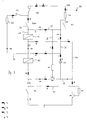
- FIGS 1 and 2 show a circuit monitoring 1.
- the monitoring circuit 1 includes four signal inputs Z1, Z2, Z3 and Z4. Each signal input Z1, Z2, Z3 and Z4 is connected to a resistance 2.
- Figures 1 and 2 show a line of positive energy 3 and a line of negative energy 4.
- Signal input Z1 is connected by via a line 5 with the transmitter side of a V185 transistor.
- the base of the transistor is connected, on the one hand, via a line 6 to the positive energy line passing through a resistor 7 and, on the other hand, to the collector of a transistor V189, which transistor V189 is connected by its emitter to the negative energy line 4 and by its base at the entrance of Z2 signals passing through a resistor 2.
- Transistor V185 communicates through its collector with the base of a transistor V181, which is connected by its transmitter at negative energy line 4, for through a line 8, and is connected by its one line collector 9.
- a resistor 10 is mounted in line 9, which resistor rose parallel with a capacitor C43, the capacitor being designed as an electrolytic capacitor polarized, whose negative plates are connected to line 9 and the positive plates to line 11.
- a transistor V179 is connected by its transmitter on line 9 and its collector on line positive energy 3.
- the base of transistor V179 is connected to the collector a V183 transistor via a line 12.
- the transistor V183 is, for its part, connected by its base with the collector of a transistor V193, of which the transmitter is connected to line 5 and whose base is connected via line 13 to the collector of a transistor V191.
- the transistor V191 is connected by its transmitter with the negative energy line 4 and by its base with the collector of a transistor V204, by through a line 14.
- the base of the transistor V204 is connected to line 6 via a diode from Zener.
- the transistors V189, V181, V179, V193 and V204 are designed as NPN transistors, while the transistors V191, V183 and V185 are designed as PNP transistors.
- Line 11 connects line 15 with a line 16, which will be further described below.
- Line 15 communicates with the transmitter of transistor V183 and with the emitter of a transistor V145.
- line 15 is connected to line 17, in which two relays K1 and K2 are connected in series and which is also connected to the power line positive 3.
- a diode 18 is mounted in line 17.
- Another diode 19 is mounted in line 11.
- the right side of the monitoring circuit, above described, is reproduced analogously in the left side of monitoring circuit 1 for signal inputs Z3 and Z4.
- the signal input Z3 is connected via line 20, in which resistor 2 is mounted, with the transmitter a transistor V161, which transistor V161 is connected via line 21 with the collector of a transistor V165.
- a line 22 At the base of transistor V165 is connected a line 22, which connects the base of the transistor V165 with signal input Z4.
- the V165 transistor is connected by its transmitter with the power line negative 4.
- line 21 communicates with a line 23, in which a resistor 24 is mounted and which is connected to the positive energy line 3.
- the collector of transistor V161 is connected to the base of a V169 collector, the transmitter of which is connected via a line 25 with the line of negative energy 4 and whose collector is mounted in series with a resistor 26 and a capacitor C41.
- the capacitor C41 is, for its part, designed as a polarized electrolytic capacitor, including the plate positive is connected via line 27 with line 9, a diode 28 being mounted in the line 27.
- Line 27 is also connected to line 15 via line 29, in which is mounted a diode 30.
- transistor V167 Between capacitor C41 and resistor 26, is mounted the emitter of a transistor V167, the collector is connected to the positive energy line 3 and whose base is connected to the emitter of the transistor V145, previously mentioned.
- the transistor V145 is - as already mentioned - connected by its transmitter with line 15.
- the base of transistor V145 communicates with the collector of a transistor V141, of which the transmitter is connected to line 20.
- the base of the transistor V141 is connected to the collector of a transistor V137 which, for its part, is connected by its transmitter with positive energy line 3.
- the basis of the transistor V137 communicates with the collector of a transistor V136, the base of which is connected to line 23 passing through a Zener diode 31, the resistance 24 being connected in series with the diode 31.
- Figure 1 shows a first phase of the monitoring with the load current, the discharge of relays and control current.
- the charging current is additionally marked with an arrow with the number 1, the discharge current of the relays by an arrow with the number 2 and the current of command by an arrow with the number 3.
- signal inputs Z3 and Z4 receive positive potential and signal inputs Z1 and Z2 capture zero potential.
- Capacitor C43 is charged and capacitor C41 is discharged.
- Transistors V161, V165 and V169 are controlled directly by the potentials captured at the inputs of signals Z3 and Z4. The corresponding charge currents are routed by lines 20, 21 and 22.
- the zero potentials of signal inputs Z1 and Z2 cause the transistor V204 to be conductive.
- This transistor V204 allows the current to be routed to the base of transistor V191, whose collector controls also the base of transistor V193.
- the transistor V193 is conductive on the sole condition that the input of signals Z1 picks up zero potential.
- the base current of transistor V183 which is supplied by the capacitor C43, passes through the transistor V193.
- the base current of transistor V179 is supplied by via the collector-emitter path of the transistor V183.
- the transistors V169 and V179 are used so that the capacitor C43 sends a discharge current in relays K1 and K2.
- the discharge is carried out via the transistor V179, the discharge also providing the basic current for transistors V179 and V183.
- Capacitor C41 is charged via transistors V179 and V169 at the same time as operating the discharge of capacitor C43.
- the loading of capacitor C41 results from the potential picked up at the inputs Z3 and Z4 signals.
- the V181 transistors, V185 and V189 are controlled directly, given that in this case the signal inputs Z1 and Z2 have potential and the signal inputs Z3 and Z4 have zero potential.
- the null potentials of signal inputs Z3 and Z4 cause the transistor V136 is conductive.
- This transistor V136 allows the current to be routed to the base of the transistor V137, the collector of which also controls the base of transistor V141.
- the transistor V141 is driver on the sole condition that the input of signals Z3 captures zero potential.
- the base current of transistor V145 which is supplied by capacitor C41, passes through the transistor V141.
- the base current of transistor V167 is routed via the collector-emitter path of transistor V145.
- the transistors V167 and V181 are used.
- the capacitor C41 sends a discharge current in relays K1 and K2 by through transistor V167.
- the capacitor C41 provides the base current for the transistors V167 and V145.
- Capacitor C43 is charged via transistors V167 and V181 at the same time as the discharge of the capacitor takes place C41.
- Figure 3 shows line 17 in which are mounted relays K1 and K2.
- a V65 diode is mounted in series between the two relays K1 and K2.
- Resistance 33 and a V53 diode are connected in parallel with respect to at relay K1.
- a working contact of relay K1 is mounted upstream of resistor 33.
- the relay K2 working contact is fitted in series with a switch 34 for controlling starting external.
- K2 relay break contact is fitted in line 17, while the break contact of the relay K1 is mounted in a line 35 connected to the line 17, which line 35 is connected via of a resistance R49 at the working contact of the relay K2.
- a V83 diode is mounted in the line 35, the break contact being disposed between the resistor R49 and diode V83.
- a V86 diode and a capacitor C15 are mounted in a line 36 connected between resistance R49 and contact of relay K1 broken. Between capacitor C15 and diode V86, line 36 is connected to line 37 which, on the one hand, is connected to line 17 and, on the other hand, is connected to resistor 33.
- Line 36 Parallel to line 36 is a line 38 which connects line 35 with a transistor V85, the line 38 being connected to the base of transistor V85.
- transistor V85 By its collector, transistor V85 is connected to line 17 between relay K2 and the relay break contact K2, while the emitter of transistor V85 communicates with a line 39, which communicates itself with the line 36, in which the capacitor C15 is mounted.
- Line 39 is also connected via a line 40 with line 17, between the two relays K1 and K2.
- Line 41 in which a resistance R57, is arranged parallel to the line 39.
- Line 41 connects line 17 with the base of a transistor V91, whose collector communicates with the line 40.
- the external start-up process is divided into four phases, which must be carried out one after the other.
- the four phases are represented in FIG. 3 by the currents i 1 , i 2 , i 3 and i 4 , arrows identified by the capitals A to D being assigned to the currents i n .
- the capacitor C15 is charged via opening contacts of the two relays K1 and K2. On this occasion, the current base of transistor V91 crosses relay K2. The charging of capacitor C15 is necessary for ability to use relay K2.
- the switch 34 is actuated so as to energize relay K1. The current crosses then the relay K1 and the transistor V91. This phase constitutes the start instruction.
- relay K1 When, after the start instruction, the relay K1 is put in the self-maintenance position, the current through resistance R49, relay K1 and transistor V91. The working contact of relay K1 controls the base of transistor V85 for this purpose. From this done, the capacitor C15 is discharged by the relay K2. Capacitor C15 continues to supply the transistor V85 with additional base current. During this third phase, relay K1 is in self-maintenance position.
- the relay K2 is energized. As soon as relay K2 has been excited, transistor V91 is closed and the current of holding through the closing contacts of the two relay K1 and K2.
- this type of startup is less expensive, more efficient and provides total surveillance not only of the circuit 32, but also of the machine mounted in downstream of this circuit.
Landscapes
- Engineering & Computer Science (AREA)
- General Engineering & Computer Science (AREA)
- Mechanical Engineering (AREA)
- Physics & Mathematics (AREA)
- General Physics & Mathematics (AREA)
- Automation & Control Theory (AREA)
- Relay Circuits (AREA)
- Alarm Systems (AREA)
- Burglar Alarm Systems (AREA)
Applications Claiming Priority (2)
| Application Number | Priority Date | Filing Date | Title |
|---|---|---|---|
| DE19715098A DE19715098B4 (de) | 1997-04-11 | 1997-04-11 | Überwachungsschaltung |
| DE19715098 | 1997-04-11 |
Publications (3)
| Publication Number | Publication Date |
|---|---|
| EP0874383A2 true EP0874383A2 (de) | 1998-10-28 |
| EP0874383A3 EP0874383A3 (de) | 2004-06-23 |
| EP0874383B1 EP0874383B1 (de) | 2006-05-31 |
Family
ID=7826190
Family Applications (1)
| Application Number | Title | Priority Date | Filing Date |
|---|---|---|---|
| EP98400885A Expired - Lifetime EP0874383B1 (de) | 1997-04-11 | 1998-04-09 | Überwachungsschaltung |
Country Status (4)
| Country | Link |
|---|---|
| US (1) | US5999395A (de) |
| EP (1) | EP0874383B1 (de) |
| JP (1) | JP4176185B2 (de) |
| DE (1) | DE19715098B4 (de) |
Families Citing this family (8)
| Publication number | Priority date | Publication date | Assignee | Title |
|---|---|---|---|---|
| DE19930994B4 (de) * | 1999-07-05 | 2006-03-02 | Leuze Lumiflex Gmbh + Co. Kg | Schaltungsanordnung zur Überwachung von Relais in Sicherheitsschaltungen mit mindestens 3 Relais |
| DE10011211B4 (de) † | 2000-03-08 | 2004-08-05 | Pilz Gmbh & Co. | Sicherheitsschaltgerät und Sicherheitsschaltgeräte-System |
| US6777830B1 (en) * | 2000-03-17 | 2004-08-17 | Pilz Gmbh & Company | System for reliable prevention of the restarting of a machine |
| JP2002175751A (ja) * | 2000-12-05 | 2002-06-21 | Omron Corp | リレー装置 |
| DE502004003785D1 (de) * | 2003-08-08 | 2007-06-21 | Siemens Ag | Schutzgerät zur eignung für kaskadenschaltungen und entsprechendes verfahren zum sicherheitsbedingten schalten |
| DE102008002758B4 (de) * | 2008-01-25 | 2016-04-28 | Schneider Electric Automation Gmbh | Relaisschaltung |
| WO2012116824A1 (de) * | 2011-03-02 | 2012-09-07 | Phoenix Contact Gmbh & Co. Kg | Elektromagnetisches relais mit überwachter schaltstellung |
| CN109340551A (zh) * | 2018-12-02 | 2019-02-15 | 马鞍山迪斯福工业设计有限公司 | 一种锻压机专用光电保护装置 |
Family Cites Families (14)
| Publication number | Priority date | Publication date | Assignee | Title |
|---|---|---|---|---|
| GB1258327A (de) * | 1969-05-09 | 1971-12-30 | ||
| SE372085B (de) * | 1973-02-27 | 1974-12-09 | L Svensson | |
| US4034235A (en) * | 1975-12-22 | 1977-07-05 | Product Automation And Control Limited | Circuits |
| US4054935A (en) * | 1976-05-28 | 1977-10-18 | Leon Ginsberg | Safety control circuit |
| US4157580A (en) * | 1978-01-31 | 1979-06-05 | General Signal Corporation | Fail-safe time delay circuit |
| US4257082A (en) * | 1979-11-16 | 1981-03-17 | The United States Of America As Represented By The Secretary Of The Navy | Magnetic flip-flop for hydrophone preamplifier |
| FR2631138B1 (fr) * | 1988-05-03 | 1991-04-05 | Croguennec Philippe | Dispositif de controle du demarrage d'une machine dangereuse et de protection au voisinage d'une telle machine et procede de demarrage d'une telle machine |
| DE3924693A1 (de) * | 1989-07-26 | 1991-02-14 | Phoenix Elekt | Vorrichtung zur besicherung von steuerstromkreisen, insbesondere von sps-steuerungen, als sicherheitsklemme |
| DE4134396C2 (de) * | 1990-10-30 | 1996-08-14 | Siemens Ag | Sicheres Automatisierungssystem |
| US5218196A (en) * | 1991-09-05 | 1993-06-08 | Frost Controls, Inc. | Light curtain system with system and watchdog microcontrollers |
| DE4217694A1 (de) * | 1992-05-25 | 1993-12-02 | Siemens Ag | Anordnung zur Auswertung von zwei zu einem Überwachungskreis gehörenden Spannungen |
| DE4242177A1 (de) * | 1992-12-15 | 1994-06-16 | Teves Gmbh Alfred | Schaltungsanordnung zur Überwachung einer Vielzahl von Spulen |
| DE4242792C2 (de) * | 1992-12-17 | 1997-02-06 | Sick Optik Elektronik Erwin | Sicherheitsschalteranordnung |
| ATE185448T1 (de) * | 1995-10-04 | 1999-10-15 | Schneider Electric Gmbh | Sicherheitsschaltung |
-
1997
- 1997-04-11 DE DE19715098A patent/DE19715098B4/de not_active Expired - Fee Related
-
1998
- 1998-04-09 EP EP98400885A patent/EP0874383B1/de not_active Expired - Lifetime
- 1998-04-10 US US09/058,136 patent/US5999395A/en not_active Expired - Lifetime
- 1998-04-13 JP JP10133898A patent/JP4176185B2/ja not_active Expired - Fee Related
Also Published As
| Publication number | Publication date |
|---|---|
| JPH10318492A (ja) | 1998-12-04 |
| US5999395A (en) | 1999-12-07 |
| JP4176185B2 (ja) | 2008-11-05 |
| EP0874383B1 (de) | 2006-05-31 |
| DE19715098B4 (de) | 2004-12-23 |
| DE19715098A1 (de) | 1998-10-15 |
| EP0874383A3 (de) | 2004-06-23 |
Similar Documents
| Publication | Publication Date | Title |
|---|---|---|
| EP0537084B1 (de) | Schutzschalter mit selektiver Verriegelung | |
| CA2463779C (fr) | Module de commande et de protection d'un appareil interrupteur | |
| EP0874383B1 (de) | Überwachungsschaltung | |
| EP0017892A1 (de) | Automatische Umschaltvorrichtung zum parallelen Aufladen und serienmässigen Entladen zweier Batterien | |
| EP0874437B1 (de) | Schaltung zum Start einer Maschine oder dergleichen und Verfahren zur Steuerung eines Starts einer Maschine | |
| EP0837555B1 (de) | Steuerungsvorrichtung für bürstenlosen Synchrongenerator | |
| EP3367523B1 (de) | Vorrichtung zum steuern der kontakte eines elektrischen unterbrechungsschalters | |
| EP1217711B1 (de) | Elekrisches Stromverteilungssystem und Schalter für dasselbe System | |
| EP2899826B1 (de) | Gesichertes Stromzuführungssystem | |
| EP0475800A1 (de) | Fahrzeugsicherungssystem | |
| BE1001402A3 (fr) | Dispositif de transmission et de reception de signaux de telecommande. | |
| EP3835645B1 (de) | Sicherheitsdetektor und sicherheitsdetektionssystem, das diesen sicherheitsdetektor umfasst | |
| EP1128411A1 (de) | Vorrichtung und Verfahren zur Überwachung eines elektrischen Gerätes sowie elektrische Schalttafel, versehen mit einer solchen Vorrichtung | |
| FR2653920A1 (fr) | Systeme d'alarme notamment pour vehicule automobile, a source d'energie electrique autonome. | |
| FR2587094A1 (fr) | Circuit de securite pour commander des equipements critiques de bruleurs a gaz ou a mazout | |
| FR2631138A1 (fr) | Dispositif de controle du demarrage d'une machine dangereuse et de protection au voisinage d'une telle machine et procede de demarrage d'une telle machine | |
| EP3555901A1 (de) | Anordnung eines schalters und eines hilfsaggregats | |
| FR2580056A1 (en) | Press safety circuit | |
| EP4346090A1 (de) | Motorsteuerungsvorrichtung und motorstart- und schutzsystem mit solch einer motorsteuerungsvorrichtung | |
| CH619328A5 (en) | Safety device for detecting defects in an electrical supply circuit | |
| FR2616929A1 (fr) | Dispositif de commande de test d'autonomie pour un ensemble de blocs d'eclairage de securite | |
| EP0939353A1 (de) | Hilfsvorrichtung zur Steuerung von mindestens einem elektrisch gesteuertem funktionellem Organs | |
| FR2490419A1 (fr) | Controleur de mouvements rotatifs et/ou lineaires adaptable sur toute installation ou appareil equipe d'au moins un capteur de detection de defaut du mouvement | |
| FR2630594A1 (fr) | Systeme d'alimentation pour equipement de protection numerique dans la distribution de l'electricite | |
| FR2558265A1 (fr) | Dispositif de controle de la mise en charge d'un ensemble d'accumulateurs sur un systeme de charge independant |
Legal Events
| Date | Code | Title | Description |
|---|---|---|---|
| PUAI | Public reference made under article 153(3) epc to a published international application that has entered the european phase |
Free format text: ORIGINAL CODE: 0009012 |
|
| AK | Designated contracting states |
Kind code of ref document: A2 Designated state(s): AT BE CH CY DE DK ES FI FR GB GR IE IT LI LU MC NL PT SE |
|
| AX | Request for extension of the european patent |
Free format text: AL;LT;LV;MK;RO;SI |
|
| 17P | Request for examination filed |
Effective date: 19981203 |
|
| RAP1 | Party data changed (applicant data changed or rights of an application transferred) |
Owner name: SCHNEIDER ELECTRIC INDUSTRIES SA |
|
| RAP1 | Party data changed (applicant data changed or rights of an application transferred) |
Owner name: SCHNEIDER ELECTRONIC INDUSTRIES SAS |
|
| RAP1 | Party data changed (applicant data changed or rights of an application transferred) |
Owner name: SCHNEIDER ELECTRIC INDUSTRIES SAS |
|
| PUAL | Search report despatched |
Free format text: ORIGINAL CODE: 0009013 |
|
| AK | Designated contracting states |
Kind code of ref document: A3 Designated state(s): AT BE CH CY DE DK ES FI FR GB GR IE IT LI LU MC NL PT SE |
|
| AX | Request for extension of the european patent |
Extension state: AL LT LV MK RO SI |
|
| 17Q | First examination report despatched |
Effective date: 20040830 |
|
| AKX | Designation fees paid |
Designated state(s): FR GB IT SE |
|
| REG | Reference to a national code |
Ref country code: DE Ref legal event code: 8566 |
|
| GRAP | Despatch of communication of intention to grant a patent |
Free format text: ORIGINAL CODE: EPIDOSNIGR1 |
|
| GRAS | Grant fee paid |
Free format text: ORIGINAL CODE: EPIDOSNIGR3 |
|
| GRAA | (expected) grant |
Free format text: ORIGINAL CODE: 0009210 |
|
| AK | Designated contracting states |
Kind code of ref document: B1 Designated state(s): FR GB IT SE |
|
| PG25 | Lapsed in a contracting state [announced via postgrant information from national office to epo] |
Ref country code: IT Free format text: LAPSE BECAUSE OF FAILURE TO SUBMIT A TRANSLATION OF THE DESCRIPTION OR TO PAY THE FEE WITHIN THE PRESCRIBED TIME-LIMIT;WARNING: LAPSES OF ITALIAN PATENTS WITH EFFECTIVE DATE BEFORE 2007 MAY HAVE OCCURRED AT ANY TIME BEFORE 2007. THE CORRECT EFFECTIVE DATE MAY BE DIFFERENT FROM THE ONE RECORDED. Effective date: 20060531 |
|
| REG | Reference to a national code |
Ref country code: GB Ref legal event code: FG4D Free format text: NOT ENGLISH |
|
| REG | Reference to a national code |
Ref country code: SE Ref legal event code: TRGR |
|
| GBT | Gb: translation of ep patent filed (gb section 77(6)(a)/1977) |
Effective date: 20060719 |
|
| PLBE | No opposition filed within time limit |
Free format text: ORIGINAL CODE: 0009261 |
|
| STAA | Information on the status of an ep patent application or granted ep patent |
Free format text: STATUS: NO OPPOSITION FILED WITHIN TIME LIMIT |
|
| 26N | No opposition filed |
Effective date: 20070301 |
|
| PGFP | Annual fee paid to national office [announced via postgrant information from national office to epo] |
Ref country code: GB Payment date: 20130415 Year of fee payment: 16 Ref country code: SE Payment date: 20130411 Year of fee payment: 16 |
|
| PGFP | Annual fee paid to national office [announced via postgrant information from national office to epo] |
Ref country code: IT Payment date: 20130422 Year of fee payment: 16 Ref country code: FR Payment date: 20130425 Year of fee payment: 16 |
|
| REG | Reference to a national code |
Ref country code: SE Ref legal event code: EUG |
|
| GBPC | Gb: european patent ceased through non-payment of renewal fee |
Effective date: 20140409 |
|
| REG | Reference to a national code |
Ref country code: FR Ref legal event code: ST Effective date: 20141231 |
|
| PG25 | Lapsed in a contracting state [announced via postgrant information from national office to epo] |
Ref country code: SE Free format text: LAPSE BECAUSE OF NON-PAYMENT OF DUE FEES Effective date: 20140410 Ref country code: GB Free format text: LAPSE BECAUSE OF NON-PAYMENT OF DUE FEES Effective date: 20140409 |
|
| PG25 | Lapsed in a contracting state [announced via postgrant information from national office to epo] |
Ref country code: FR Free format text: LAPSE BECAUSE OF NON-PAYMENT OF DUE FEES Effective date: 20140430 |
|
| PG25 | Lapsed in a contracting state [announced via postgrant information from national office to epo] |
Ref country code: IT Free format text: LAPSE BECAUSE OF NON-PAYMENT OF DUE FEES Effective date: 20140409 |