EP0874398A2 - Integrierte Halbleiterschaltung - Google Patents
Integrierte Halbleiterschaltung Download PDFInfo
- Publication number
- EP0874398A2 EP0874398A2 EP98107252A EP98107252A EP0874398A2 EP 0874398 A2 EP0874398 A2 EP 0874398A2 EP 98107252 A EP98107252 A EP 98107252A EP 98107252 A EP98107252 A EP 98107252A EP 0874398 A2 EP0874398 A2 EP 0874398A2
- Authority
- EP
- European Patent Office
- Prior art keywords
- substrate interconnection
- integrated circuit
- lower level
- insulating film
- semiconductor integrated
- Prior art date
- Legal status (The legal status is an assumption and is not a legal conclusion. Google has not performed a legal analysis and makes no representation as to the accuracy of the status listed.)
- Withdrawn
Links
Images


Classifications
-
- H—ELECTRICITY
- H10—SEMICONDUCTOR DEVICES; ELECTRIC SOLID-STATE DEVICES NOT OTHERWISE PROVIDED FOR
- H10P—GENERIC PROCESSES OR APPARATUS FOR THE MANUFACTURE OR TREATMENT OF DEVICES COVERED BY CLASS H10
- H10P54/00—Cutting or separating of wafers, substrates or parts of devices
-
- H—ELECTRICITY
- H10—SEMICONDUCTOR DEVICES; ELECTRIC SOLID-STATE DEVICES NOT OTHERWISE PROVIDED FOR
- H10W—GENERIC PACKAGES, INTERCONNECTIONS, CONNECTORS OR OTHER CONSTRUCTIONAL DETAILS OF DEVICES COVERED BY CLASS H10
- H10W20/00—Interconnections in chips, wafers or substrates
- H10W20/40—Interconnections external to wafers or substrates, e.g. back-end-of-line [BEOL] metallisations or vias connecting to gate electrodes
- H10W20/41—Interconnections external to wafers or substrates, e.g. back-end-of-line [BEOL] metallisations or vias connecting to gate electrodes characterised by their conductive parts
- H10W20/43—Layouts of interconnections
Definitions
- the present invention relates to a semiconductor integrated circuit, and more specifically to a semiconductor integrated circuit having a multi-level interconnection structure and an interlayer film formed by coating an organic solution of a silicon compound.
- the planarization technique includes a method for coating a SOG (spin-on-glass) solution between first level and second level aluminum layers in the case of a double-layer aluminum process.
- a coating of the SOG solution can be carried out by various methods depending upon the semiconductor device manufacturing process. For example, in one typical method, after formation of an interlayer insulating film, a wafer is rotated about a center of the wafer, and the SOG solution is dropped from an upper position, so that the SOG is distributed throughout the wafer by action of a centrifugal force of the rotation. Thereafter, the wafer is heat-treated to evaporate an organic solvent of the SOG solution and to advance the dehydration and polymerization of the silicon compound, so that a silicon oxide film is formed.
- SOG spin-on-glass
- the SOG silicon oxide film thus formed to cover the whole surface of the wafer is etched back to remove an unnecessary silicon oxide film, so that only recesses in the interlayer insulating film between the first level and second level aluminum layers are filled with the SOG silicon oxide film.
- the planarization is completed.
- a substrate interconnection is formed at the level of a first level or lower level interconnection layer, and is connected to the semiconductor substrate through a predetermined contact so that a substrate potential is supplied to the substrate.
- the substrate interconnection is formed to depict a closed loop completely surrounding a chip inner region of each semiconductor integrated circuit chip. In the periphery of each chip, therefore, a dam is built because of the thickness of the substrate interconnection layer.
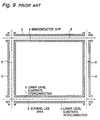
- Fig. 9 is a diagrammatic enlarged plan view illustrating the location of a lower level substrate interconnection in a semiconductor chip 5, in the prior art, and picked up from many semiconductor chips formed in a semiconductor wafer 19 as shown in Fig. 11.
- Fig. 10 is a diagrammatic partial sectional view of a substrate interconnection portion of the prior art semiconductor chip, where the SOG silicon oxide layer is deposited thickly.
- a lower level substrate interconnection 6 formed at the level of a first level interconnection layer is formed to depict a closed loop completely surrounding the chip inner region of the semiconductor chip 5, at an inside of a scribing line area 8 provided along a peripheral edge of the semiconductor chip 5.
- the lower level substrate interconnection 6 is formed to extend from the surface of the semiconductor substrate 9 to the top of a step which is formed of a field oxide film 11 and an interlayer insulating film 12 formed thereon.
- the lower level substrate interconnection 6 formed at the first level of the interconnection layer is connected to a diffused layer 17 formed at the surface of the semiconductor substrate 9 at a contact 10 between the lower level substrate interconnection 6 and the semiconductor substrate 9, for the purpose of supplying a predetermined substrate potential to the semiconductor substrate 9.
- Another interlayer insulating film 13 is formed to cover the lower level substrate interconnection 6 and the interlayer insulating film 12.
- steps are generated not only in the proximity of the scribing line area, but also on the surface of the interlayer insulating film 13 because of the thickness of the interconnection layer, depending upon whether or not the first level interconnection layer exists on the interlayer insulating film 12.
- the SOG solution is coated and dried for planarization.
- the heat treatment is carried out to form the silicon oxide film 14, and then, an unnecessary portion of the silicon oxide film is etched back.
- the SOG silicon oxide film 14 remains on the upheaved portion of the interlayer insulting film 13 caused by the thickness of the interconnection layer 6 under the second layer interlayer insulating film 13, as shown in Fig. 10.
- a third layer interlayer insulating film 15 is formed on the SOG silicon oxide film 14, and a through-hole contact 7 is formed to reach from the surface of the interlayer insulating film 15 to the lower level interconnection layer 6, for the purpose of connecting a second or upper level interconnection layer 4 to be formed after the formation of the SOG silicon oxide film, to the first or lower level interconnection layer 6 formed before the formation of the SOG silicon oxide film.
- a contact face 18 generates between the upper level substrate interconnection filling the through-hole 7 and the SOG silicon oxide film 15.
- the wafer 19 is cut off along the scribing line area 8 into individual semiconductor chips and each of the individual semiconductor chips is mounted on a lead frame or the like and encapsulated by a molding resin into a product, when moisture enters from an ambient atmosphere at the outside of the semiconductor integrated circuit through a boundary between the molding resin and the lead frame, the moisture is absorbed from the scribing line area 8 to the SOG silicon oxide film 14, to enter the inside of the semiconductor chip 5.
- the contact face 18 has generated, the moisture absorbed to the SOG silicon oxide film 14 reaches through the contact face 18 to the lower level interconnection layer 6 to corrode the lower level interconnection layer 6.
- Another object of the present invention is to provide a semiconductor integrated circuit capable of preventing corrosion of an interconnection layer caused by the moisture entering through a through-hole contact, thereby to avoid malfunction of the semiconductor integrated circuit.
- a semiconductor integrated circuit including at least two substrate interconnection layers separated from each other by an interlayer insulating film formed therebetween, an upper surface of the interlayer insulating film being coated with a silicon compound insulating film formed by coating an organic solution of a silicon compound, wherein the at least two substrate interconnection layers positioned in a predetermined scribing line area and excluding an uppermost substrate interconnection layer are divided into a plurality of segments separated from each other by gaps which are provided at a plurality of different locations and which allow the organic solution of the silicon compound to pass through the gaps when the organic solution of a silicon compound is applied.
- the uppermost substrate interconnection layer is electrically connected to the plurality of segments of the at least two substrate interconnection layers excluding the uppermost substrate interconnection layer, through contacts hole formed to penetrate through the interlayer insulating film.
- the semiconductor integrated circuit is formed on a rectangular semiconductor chip having a pair of opposing sides extending in parallel to an X coordinate axis of an X-Y coordinate and another pair of opposing sides extending in parallel to a Y coordinate axis of the X-Y coordinate, and the at least two substrate interconnection layers extend along four sides of the rectangular semiconductor chip. Furthermore, the at least two substrate interconnection layers excluding the uppermost substrate interconnection layer and extending in parallel to the X coordinate axis have the gaps located at the same X coordinate positions and the at least two substrate interconnection layers excluding the uppermost substrate interconnection layer and extending in parallel to the Y coordinate axis have the gaps located at the same Y coordinate positions.
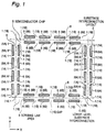
- Fig. 1 is a diagrammatic enlarged plan view illustrating the location of a lower level substrate interconnection 6 in the semiconductor integrated circuit chip 5 in a first embodiment of the present invention
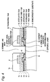
- Fig. 2 is a further enlarged partial, diagrammatic plan view of the first embodiment, illustrating a relation between an upper level substrate interconnection 4 and the lower level substrate interconnection 6, in the neighborhood of the scribing line area 8 between a pair of adjacent semiconductor chips formed in a semiconductor wafer, which is designated as a substrate interconnection layout 2 in Fig. 1.
- Figs. 3, 4 and 5 are diagrammatic sectional views taken along the line A-A, the line B-B and the line C-C in Fig. 2, respectively.
- a lower level substrate interconnection 6 formed at the level of a first level interconnection layer is formed to depict a closed loop completely surrounding an inner region of the semiconductor chip 5, at an inside of a scribing line area 8 provided along a peripheral edge of the semiconductor chip 5, but is divided into a plurality of segments (6A and 6B) separated by a plurality of gaps 1 (1A and 1B) in order to cause an SOG solution to escape by passing therebetween.
- the gaps 1 are formed at positions to oppose to each other in a pair of lower level substrate interconnections 6 which oppose to each other but which are included in a pair of adjacent different semiconductor integrated circuit chips 5, respectively.
- the rectangular semiconductor chip 5 has a pair of opposing sides extending in parallel to an X coordinate axis of an X-Y coordinate and another pair of opposing sides extending in parallel to a Y coordinate axis of the X-Y coordinate
- the substrate interconnection layers extend along four sides of the rectangular semiconductor chip
- a pair of opposing sides of the lower level substrate interconnection extending in parallel to the X coordinate axis are divided into a plurality of segments (6B) separated by the gaps (1B) located at the same X coordinate positions
- another pair of opposing sides of the lower level substrate interconnection extending in parallel to the Y coordinate axis are divided into a plurality of segments (6A) separated by the gaps (1A) located at the same Y coordinate positions.
- the lower level substrate interconnection are cut out at four corners of the rectangular semiconductor chip 5 so that the gaps 1 are formed at the four corners of the rectangular semiconductor chip 5.
- the lower level substrate interconnections 6 divided into a plurality of segments by the gaps 1 are connected through through-hole contacts 7 to the upper level substrate interconnections 4 which can be formed to depict a closed loop completely surrounding the inner region of the semiconductor chip 5, at an inside of the scribing line area 8.
- the lower level substrate interconnection 6 is connected through a contact 10 to a semiconductor substrate 9 as shown in Fig. 3, and also connected to a pad (not shown) or a substrate potential generating circuit (not shown) in order to supply a necessary potential to the semiconductor substrate 9.
- the lower level substrate interconnection 6 is not required to completely circulate around the inner region of the semiconductor chip 5, and therefore, can be cut off in the way.
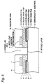
- Fig. 3 illustrates a lateral and vertical positional relation between the upper level substrate interconnection 4, the lower level substrate interconnection 6, the through-hole contact 7, the scribing line area 8, the semiconductor substrate 9, the contact 10, a field oxide film 11, interlayer insulating films 12, 13 and 15, an SOG silicon oxide film 14, a passivation film 16, and a diffused layer 17.
- the interlayer insulating film 12 is formed between the lower level substrate interconnection 6 and the field oxide film 11, and the lower level substrate interconnection 6 is formed on the interlayer insulating film 12 to partially ride on an outer edge portion of the field oxide film 11.
- the interlayer insulating film 12 is partially removed by an etching in a contact formation process, so that the lower level substrate interconnection 6 is electrically connected through the contact 10 to the diffused layer 17 formed at a surface of the semiconductor substrate 9.
- the interlayer insulating film 13 is formed to cover the lower level substrate interconnection 6 and the interlayer insulating film 12, and the SOG silicon oxide film 14 is formed to fill recesses formed on the surface of the interlayer insulating film 13 to planarize the whole surface.
- the SOG silicon oxide film 14 does not remain on the interlayer insulating film 13 covering the portion of the lower level substrate interconnection 6 riding on the field oxide film 11.
- the interlayer insulating film 15 is formed to cover the SOG silicon oxide film 14 and the interlayer insulating film 13 covering the lower level substrate interconnection 6.
- the upper level substrate interconnection 4 is formed on the interlayer insulating film 15, and is connected to the lower level substrate interconnection 6 through the through-hole contact 7 which is formed to penetrate through only the interlayer insulating films 15 and 13 to reach the lower level substrate interconnection 6.
- the SOG silicon oxide film 14 does not remain on the interlayer insulating film 13 covering the portion of the lower level substrate interconnection 6 riding on the field oxide film 11, the upper level substrate interconnection 4 never contacts to the SOG silicon oxide film 14 in the through-hole contact 7.
- the passivation film 16 is a surface protection film for covering the semiconductor chip 5.
- Fig. 4 is a sectional view taken along the line B-B passing through position where the through-hole contact 7 is not formed in Fig. 2.
- Fig. 4 illustrates a lateral and vertical positional relation between the upper level substrate interconnection 4, the lower level substrate interconnection 6, the scribing line area 8, the semiconductor substrate 9, the contact 10, the field oxide film 11, the interlayer insulating films 12, 13 and 15, the SOG silicon oxide film 14, the passivation film 16, and the diffused layer 17. Since Fig. 4 is similar to Fig. 3, excepting for the through-hole contact 7, a further explanation will be omitted for simplification of the description.
- Fig. 5 is a sectional view taken along the line C-C passing through a position of the gap 6, namely, a position where the lower level substrate interconnection 6 is not formed in Fig. 2.
- Fig. 5 illustrates a lateral and vertical positional relation between the upper level substrate interconnection 4, the scribing line area 8, the semiconductor substrate 9, the field oxide film 11, the interlayer insulating films 12, 13 and 15, the SOG silicon oxide film 14, the passivation film 16, and the diffused layer 17. Since Fig. 5 is similar to Fig. 3, excepting that the through-hole contact 7, the lower level substrate interconnection 6, and the contact 10 are not formed, a further explanation will be omitted for simplification of the description. As seen from Fig. 5, at a position of the gap 1, no step is generated by the lower level substrate interconnection 6.
- the semiconductor chip 5 shown in Fig. 1 is one picked up from many semiconductor chips formed in a semiconductor wafer 19 as shown in Fig. 11.
- the SOG solution is dropped from an upper nozzle onto the wafer 19 which is supported by a rotating rotary table and which therefore is rotating together with the rotary table, as well known to person skilled in the art.
- the SOG solution dropped on the wafer is spread to an outer edge of the wafer by action of a centrifugal force of the rotation.
- the rotational speed of the wafer and the amount of the SOG solution dropped on the wafer are previously determined to realize an optimum thickness of the SOG film.
- the SOG solution dropped on the wafer is uniformly distributed throughout the wafer by action of a centrifugal force of the rotation.
- the centrifugal force caused by the rotation of the wafer 19 acts on the chip 5 in a left direction in the drawing, so that the SOG solution also moves in the left direction in the drawing, to fill up recesses formed on the interlayer insulating film covering the lower level substrate interconnection 6.
- the SOG solution reaches on the lower level substrate interconnection 6 formed on the periphery of the semiconductor chip 5
- an excessive SOG solution is caused to escape from the semiconductor chip 5 through the gaps 1 between the divided segments of the lower level substrate interconnection.
- This advantage is further elevated if the lower level substrate interconnection are cut out at four comers of the rectangular semiconductor chip 5 so that the gaps 1 are formed at the four comers of the rectangular semiconductor chip 5, as shown in Fig. 1.
- the gaps 1 formed in mutually adjacent lower level substrate interconnections of each pair of adjacent different semiconductor chips are located to be symmetrical with a center line of the scribing line area 8, namely, to align with each other at the same coordinate positions as mentioned hereinbefore.
- the excessive SOG solution flows and moves from the gaps 1 of one semiconductor chip through the scribing line area 8 into the gaps of adjacent another semiconductor chip.
- the SOG solution can be uniformly coated throughout all the semiconductor chips in one wafer.
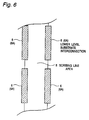
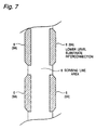
- the divided segments (6A and 6B) of the lower level substrate interconnections can be formed in any shape, which includes any polygon including a rectangle or a trapezoid, as shown in Figs. 6 and 7, which are partial enlarged views of adjacent different lower level substrate interconnections separated by the scribing line area.
- the shape of the gaps 1 can take any shape in accordance with the shape of the divided segments (6A and 6B) of the lower level substrate interconnection 6.
- the SOG silicon oxide film 14 no longer remains on the upheaved portion of the interlayer insulating film 13 covering the portion of the lower level substrate interconnection 6 riding on the field oxide film 11, as shown in Figs. 3, 4 and 5. Therefore, the interlayer insulating film 15 is deposited directly on the upheaved portion of the interlayer insulating film 13 covering the portion of the lower level substrate interconnection 6 riding on the field oxide film 11, as shown in Figs. 3, 4 and 5.
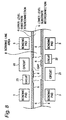
- FIG. 8 is an enlarged partial, diagrammatic plan view illustrating the layout of the neighborhood of the scribing line area 8 between adjacent different semiconductor chips, a second embodiment of the semiconductor integrated circuit chip in accordance with the present invention will be described.
- Fig. 8 illustrates a partial layout of substrate interconnections between a semiconductor chip including internal circuits 23 and 20 and bonding pads 3 and an adjacent semiconductor chip including internal circuits 21 and 22 and bonding pads 3.
- the gaps 1 formed in the respective lower level substrate interconnections 6 are located to correspond to the positions of the internal circuits 20 to 23 provided in the respective semiconductor chips.
- These internal circuits 20 to 23 include interconnection layers which connect to transistors and/or between transistors and which are located at the same level as that of the substrate interconnections.
- the gaps 1 are provided in the lower level substrate interconnections, at the positions in the neighborhood of the internal circuits 20 to 23, the excessive SOG solution can be taken out or removed, so that a thick SOG silicon oxide film 14 is prevented from remaining in the inside of the internal circuits 20 to 23.
- the malfunction of the semiconductor integrated circuit is avoided, so that the reliability can be elevated.
- the internal circuits 20 to 23 can be located near to the lower level substrate interconnections 6, the size of the semiconductor chip can be reduced.
- the semiconductor integrated circuit in accordance with the present invention since a plurality of gaps are formed in the lower level substrate interconnection located at a periphery of the semiconductor chip to surround the internal region of the semiconductor chip, an excessive SOG solution can be removed from the neighborhood of the lower level substrate interconnection when the SOG solution is coated on the wafer. Therefore, it is possible to prevent the corrosion of the interconnection caused by the moisture which, in the prior art, entered through the through-hole contact and through the SOG silicon oxide film remaining on the step or upheaved portion formed by the lower level substrate interconnection. Accordingly, the malfunction of the semiconductor integrated circuit is prevented, and the reliability of the semiconductor integrated circuit can be elevated.
- the internal circuits are located near to the gaps formed in the lower level substrate interconnection located at the periphery of the semiconductor chip to surround the internal region of the semiconductor chip, the internal circuits can be located near to the lower level substrate interconnection, with the result that the size of the semiconductor chip can be reduced.
Landscapes
- Internal Circuitry In Semiconductor Integrated Circuit Devices (AREA)
Applications Claiming Priority (3)
| Application Number | Priority Date | Filing Date | Title |
|---|---|---|---|
| JP103096/97 | 1997-04-21 | ||
| JP10309697 | 1997-04-21 | ||
| JP09103096A JP3098450B2 (ja) | 1997-04-21 | 1997-04-21 | 半導体集積回路 |
Publications (2)
| Publication Number | Publication Date |
|---|---|
| EP0874398A2 true EP0874398A2 (de) | 1998-10-28 |
| EP0874398A3 EP0874398A3 (de) | 1999-10-13 |
Family
ID=14345111
Family Applications (1)
| Application Number | Title | Priority Date | Filing Date |
|---|---|---|---|
| EP98107252A Withdrawn EP0874398A3 (de) | 1997-04-21 | 1998-04-21 | Integrierte Halbleiterschaltung |
Country Status (6)
| Country | Link |
|---|---|
| US (1) | US5892284A (de) |
| EP (1) | EP0874398A3 (de) |
| JP (1) | JP3098450B2 (de) |
| KR (1) | KR100283300B1 (de) |
| CN (1) | CN1113394C (de) |
| TW (1) | TW393696B (de) |
Cited By (1)
| Publication number | Priority date | Publication date | Assignee | Title |
|---|---|---|---|---|
| EP0899788A3 (de) * | 1997-08-29 | 2000-09-13 | Nec Corporation | Halbleiteranordnung und Verfahren mit verbesserter flacher Oberfläche |
Families Citing this family (4)
| Publication number | Priority date | Publication date | Assignee | Title |
|---|---|---|---|---|
| JP4742407B2 (ja) * | 2000-07-17 | 2011-08-10 | ソニー株式会社 | 半導体装置とその製造方法 |
| US8643147B2 (en) * | 2007-11-01 | 2014-02-04 | Taiwan Semiconductor Manufacturing Company, Ltd. | Seal ring structure with improved cracking protection and reduced problems |
| US7906836B2 (en) * | 2008-11-14 | 2011-03-15 | Taiwan Semiconductor Manufacturing Company, Ltd. | Heat spreader structures in scribe lines |
| JP5275523B2 (ja) * | 2010-11-04 | 2013-08-28 | シャープ株式会社 | 表示装置、ならびに半導体装置および表示装置の製造方法 |
Citations (3)
| Publication number | Priority date | Publication date | Assignee | Title |
|---|---|---|---|---|
| JPS6018934A (ja) * | 1983-07-13 | 1985-01-31 | Hitachi Micro Comput Eng Ltd | 半導体装置 |
| JPH08306771A (ja) * | 1995-04-27 | 1996-11-22 | Yamaha Corp | 半導体装置とその製造方法 |
| US5593925A (en) * | 1993-07-24 | 1997-01-14 | Yamaha Corporation | Semiconductor device capable of preventing humidity invasion |
Family Cites Families (9)
| Publication number | Priority date | Publication date | Assignee | Title |
|---|---|---|---|---|
| JP2856489B2 (ja) * | 1990-03-19 | 1999-02-10 | 富士通株式会社 | 半導体装置の製造方法 |
| JPH05190689A (ja) * | 1992-01-09 | 1993-07-30 | Yamaha Corp | 多層配線形成法 |
| US5441915A (en) * | 1992-09-01 | 1995-08-15 | Taiwan Semiconductor Manufacturing Company Ltd. | Process of fabrication planarized metallurgy structure for a semiconductor device |
| JPH0714806A (ja) * | 1993-06-15 | 1995-01-17 | Nec Yamaguchi Ltd | 半導体集積回路装置 |
| JP2755131B2 (ja) * | 1993-10-27 | 1998-05-20 | 日本電気株式会社 | 半導体装置 |
| US5602423A (en) * | 1994-11-01 | 1997-02-11 | Texas Instruments Incorporated | Damascene conductors with embedded pillars |
| US5757077A (en) * | 1995-02-03 | 1998-05-26 | National Semiconductor Corporation | Integrated circuits with borderless vias |
| JPH0955425A (ja) * | 1995-08-10 | 1997-02-25 | Mitsubishi Electric Corp | 多層Al配線構造を有する半導体装置およびその製造方法 |
| US5847464A (en) * | 1995-09-27 | 1998-12-08 | Sgs-Thomson Microelectronics, Inc. | Method for forming controlled voids in interlevel dielectric |
-
1997
- 1997-04-21 JP JP09103096A patent/JP3098450B2/ja not_active Expired - Fee Related
-
1998
- 1998-04-20 TW TW087106208A patent/TW393696B/zh not_active IP Right Cessation
- 1998-04-20 KR KR1019980014025A patent/KR100283300B1/ko not_active Expired - Fee Related
- 1998-04-21 CN CN98109259A patent/CN1113394C/zh not_active Expired - Fee Related
- 1998-04-21 EP EP98107252A patent/EP0874398A3/de not_active Withdrawn
- 1998-04-21 US US09/063,712 patent/US5892284A/en not_active Expired - Fee Related
Patent Citations (4)
| Publication number | Priority date | Publication date | Assignee | Title |
|---|---|---|---|---|
| JPS6018934A (ja) * | 1983-07-13 | 1985-01-31 | Hitachi Micro Comput Eng Ltd | 半導体装置 |
| US5593925A (en) * | 1993-07-24 | 1997-01-14 | Yamaha Corporation | Semiconductor device capable of preventing humidity invasion |
| JPH08306771A (ja) * | 1995-04-27 | 1996-11-22 | Yamaha Corp | 半導体装置とその製造方法 |
| US5763936A (en) * | 1995-04-27 | 1998-06-09 | Yamaha Corporation | Semiconductor chip capable of supressing cracks in insulating layer |
Cited By (2)
| Publication number | Priority date | Publication date | Assignee | Title |
|---|---|---|---|---|
| EP0899788A3 (de) * | 1997-08-29 | 2000-09-13 | Nec Corporation | Halbleiteranordnung und Verfahren mit verbesserter flacher Oberfläche |
| US6538301B1 (en) | 1997-08-29 | 2003-03-25 | Nec Corporation | Semiconductor device and method with improved flat surface |
Also Published As
| Publication number | Publication date |
|---|---|
| CN1113394C (zh) | 2003-07-02 |
| EP0874398A3 (de) | 1999-10-13 |
| KR19980081549A (ko) | 1998-11-25 |
| JPH10294363A (ja) | 1998-11-04 |
| CN1199241A (zh) | 1998-11-18 |
| US5892284A (en) | 1999-04-06 |
| JP3098450B2 (ja) | 2000-10-16 |
| TW393696B (en) | 2000-06-11 |
| KR100283300B1 (ko) | 2001-04-02 |
Similar Documents
| Publication | Publication Date | Title |
|---|---|---|
| US12057362B2 (en) | Semiconductor device and method for manufacturing semiconductor device | |
| US7285867B2 (en) | Wiring structure on semiconductor substrate and method of fabricating the same | |
| US7633159B2 (en) | Semiconductor device assemblies and packages with edge contacts and sacrificial substrates and other intermediate structures used or formed in fabricating the assemblies or packages | |
| US4576900A (en) | Integrated circuit multilevel interconnect system and method | |
| US11705341B2 (en) | Method of fabricating a semiconductor package having redistribution patterns including seed patterns and seed layers | |
| US20220045033A1 (en) | Semiconductor package and method of fabricating the same | |
| US20250149418A1 (en) | Semiconductor package and method of fabricating the same | |
| US7741725B2 (en) | Semiconductor apparatus and method of producing the same | |
| US20250364489A1 (en) | Semiconductor package | |
| CN220021087U (zh) | 半导体封装体 | |
| US20260026394A1 (en) | Package and Method for Forming the Same | |
| US20240128214A1 (en) | Integrated circuit structure | |
| US5892284A (en) | Semiconductor integrated circuit | |
| KR19990024021A (ko) | 개선된 평탄한 표면을 가진 반도체 장치 및 그 제조 방법 | |
| US6294454B1 (en) | Method for manufacturing a bed structure underlying electrode pad of semiconductor device | |
| CN115084076A (zh) | 半导体封装结构及其制法 | |
| US12616055B2 (en) | Semiconductor device and method for making the same | |
| KR102933597B1 (ko) | 재배선층을 포함하는 반도체 장치 및 그 제조 방법 | |
| US20250226361A1 (en) | Semiconductor package | |
| JP3038904B2 (ja) | 半導体集積回路 | |
| CN119069457A (zh) | 半导体封装件 | |
| KR980011851A (ko) | 홀 비아(Hole Via)를 이용한 다층 금속 배선의 금속층간 접속 구조 및 본딩 패드 |
Legal Events
| Date | Code | Title | Description |
|---|---|---|---|
| PUAI | Public reference made under article 153(3) epc to a published international application that has entered the european phase |
Free format text: ORIGINAL CODE: 0009012 |
|
| AK | Designated contracting states |
Kind code of ref document: A2 Designated state(s): DE FR GB |
|
| AX | Request for extension of the european patent |
Free format text: AL;LT;LV;MK;RO;SI |
|
| PUAL | Search report despatched |
Free format text: ORIGINAL CODE: 0009013 |
|
| AK | Designated contracting states |
Kind code of ref document: A3 Designated state(s): AT BE CH CY DE DK ES FI FR GB GR IE IT LI LU MC NL PT SE |
|
| AX | Request for extension of the european patent |
Free format text: AL;LT;LV;MK;RO;SI |
|
| RIC1 | Information provided on ipc code assigned before grant |
Free format text: 6H 01L 21/78 A, 6H 01L 23/528 B, 6H 01L 21/768 B |
|
| 17P | Request for examination filed |
Effective date: 20000105 |
|
| AKX | Designation fees paid |
Free format text: DE FR GB |
|
| 17Q | First examination report despatched |
Effective date: 20020208 |
|
| RAP1 | Party data changed (applicant data changed or rights of an application transferred) |
Owner name: NEC ELECTRONICS CORPORATION |
|
| STAA | Information on the status of an ep patent application or granted ep patent |
Free format text: STATUS: THE APPLICATION IS DEEMED TO BE WITHDRAWN |
|
| 18D | Application deemed to be withdrawn |
Effective date: 20030917 |