EP0875331A2 - Weichlotlegierung und mit einer Weichlotlegierung versehenes Substrat zum Montieren von elektronischen Bauteilen: Substrat mit Anordnung eines elektronischen Bauteils - Google Patents
Weichlotlegierung und mit einer Weichlotlegierung versehenes Substrat zum Montieren von elektronischen Bauteilen: Substrat mit Anordnung eines elektronischen Bauteils Download PDFInfo
- Publication number
- EP0875331A2 EP0875331A2 EP97116635A EP97116635A EP0875331A2 EP 0875331 A2 EP0875331 A2 EP 0875331A2 EP 97116635 A EP97116635 A EP 97116635A EP 97116635 A EP97116635 A EP 97116635A EP 0875331 A2 EP0875331 A2 EP 0875331A2
- Authority
- EP
- European Patent Office
- Prior art keywords
- substrate
- solder
- zinc
- component
- bonding
- Prior art date
- Legal status (The legal status is an assumption and is not a legal conclusion. Google has not performed a legal analysis and makes no representation as to the accuracy of the status listed.)
- Granted
Links
Images


Classifications
-
- H—ELECTRICITY
- H05—ELECTRIC TECHNIQUES NOT OTHERWISE PROVIDED FOR
- H05K—PRINTED CIRCUITS; CASINGS OR CONSTRUCTIONAL DETAILS OF ELECTRIC APPARATUS; MANUFACTURE OF ASSEMBLAGES OF ELECTRICAL COMPONENTS
- H05K3/00—Apparatus or processes for manufacturing printed circuits
- H05K3/30—Assembling printed circuits with electric components, e.g. with resistors
- H05K3/32—Assembling printed circuits with electric components, e.g. with resistors electrically connecting electric components or wires to printed circuits
- H05K3/34—Assembling printed circuits with electric components, e.g. with resistors electrically connecting electric components or wires to printed circuits by soldering
- H05K3/346—Solder materials or compositions specially adapted therefor
-
- B—PERFORMING OPERATIONS; TRANSPORTING
- B23—MACHINE TOOLS; METAL-WORKING NOT OTHERWISE PROVIDED FOR
- B23K—SOLDERING OR UNSOLDERING; WELDING; CLADDING OR PLATING BY SOLDERING OR WELDING; CUTTING BY APPLYING HEAT LOCALLY, e.g. FLAME CUTTING; WORKING BY LASER BEAM
- B23K35/00—Rods, electrodes, materials, or media, for use in soldering, welding, or cutting
- B23K35/22—Rods, electrodes, materials, or media, for use in soldering, welding, or cutting characterised by the composition or nature of the material
- B23K35/24—Selection of soldering or welding materials proper
- B23K35/26—Selection of soldering or welding materials proper with the principal constituent melting at less than 400°C
- B23K35/262—Sn as the principal constituent
-
- H—ELECTRICITY
- H05—ELECTRIC TECHNIQUES NOT OTHERWISE PROVIDED FOR
- H05K—PRINTED CIRCUITS; CASINGS OR CONSTRUCTIONAL DETAILS OF ELECTRIC APPARATUS; MANUFACTURE OF ASSEMBLAGES OF ELECTRICAL COMPONENTS
- H05K1/00—Printed circuits
- H05K1/02—Details
- H05K1/11—Printed elements for providing electric connections to or between printed circuits
- H05K1/111—Pads for surface mounting, e.g. lay-out
-
- H—ELECTRICITY
- H10—SEMICONDUCTOR DEVICES; ELECTRIC SOLID-STATE DEVICES NOT OTHERWISE PROVIDED FOR
- H10W—GENERIC PACKAGES, INTERCONNECTIONS, CONNECTORS OR OTHER CONSTRUCTIONAL DETAILS OF DEVICES COVERED BY CLASS H10
- H10W72/00—Interconnections or connectors in packages
- H10W72/20—Bump connectors, e.g. solder bumps or copper pillars; Dummy bumps; Thermal bumps
-
- H—ELECTRICITY
- H05—ELECTRIC TECHNIQUES NOT OTHERWISE PROVIDED FOR
- H05K—PRINTED CIRCUITS; CASINGS OR CONSTRUCTIONAL DETAILS OF ELECTRIC APPARATUS; MANUFACTURE OF ASSEMBLAGES OF ELECTRICAL COMPONENTS
- H05K2201/00—Indexing scheme relating to printed circuits covered by H05K1/00
- H05K2201/09—Shape and layout
- H05K2201/09209—Shape and layout details of conductors
- H05K2201/09654—Shape and layout details of conductors covering at least two types of conductors provided for in H05K2201/09218 - H05K2201/095
- H05K2201/098—Special shape of the cross-section of conductors, e.g. very thick plated conductors
-
- H—ELECTRICITY
- H05—ELECTRIC TECHNIQUES NOT OTHERWISE PROVIDED FOR
- H05K—PRINTED CIRCUITS; CASINGS OR CONSTRUCTIONAL DETAILS OF ELECTRIC APPARATUS; MANUFACTURE OF ASSEMBLAGES OF ELECTRICAL COMPONENTS
- H05K2201/00—Indexing scheme relating to printed circuits covered by H05K1/00
- H05K2201/10—Details of components or other objects attached to or integrated in a printed circuit board
- H05K2201/10613—Details of electrical connections of non-printed components, e.g. special leads
- H05K2201/10621—Components characterised by their electrical contacts
- H05K2201/10689—Leaded Integrated Circuit [IC] package, e.g. dual-in-line [DIL]
-
- H—ELECTRICITY
- H05—ELECTRIC TECHNIQUES NOT OTHERWISE PROVIDED FOR
- H05K—PRINTED CIRCUITS; CASINGS OR CONSTRUCTIONAL DETAILS OF ELECTRIC APPARATUS; MANUFACTURE OF ASSEMBLAGES OF ELECTRICAL COMPONENTS
- H05K3/00—Apparatus or processes for manufacturing printed circuits
- H05K3/30—Assembling printed circuits with electric components, e.g. with resistors
- H05K3/32—Assembling printed circuits with electric components, e.g. with resistors electrically connecting electric components or wires to printed circuits
- H05K3/34—Assembling printed circuits with electric components, e.g. with resistors electrically connecting electric components or wires to printed circuits by soldering
- H05K3/341—Surface mounted components
- H05K3/3421—Leaded components
-
- H—ELECTRICITY
- H10—SEMICONDUCTOR DEVICES; ELECTRIC SOLID-STATE DEVICES NOT OTHERWISE PROVIDED FOR
- H10W—GENERIC PACKAGES, INTERCONNECTIONS, CONNECTORS OR OTHER CONSTRUCTIONAL DETAILS OF DEVICES COVERED BY CLASS H10
- H10W90/00—Package configurations
- H10W90/701—Package configurations characterised by the relative positions of pads or connectors relative to package parts
- H10W90/721—Package configurations characterised by the relative positions of pads or connectors relative to package parts of bump connectors
- H10W90/724—Package configurations characterised by the relative positions of pads or connectors relative to package parts of bump connectors between a chip and a stacked insulating package substrate, interposer or RDL
-
- Y—GENERAL TAGGING OF NEW TECHNOLOGICAL DEVELOPMENTS; GENERAL TAGGING OF CROSS-SECTIONAL TECHNOLOGIES SPANNING OVER SEVERAL SECTIONS OF THE IPC; TECHNICAL SUBJECTS COVERED BY FORMER USPC CROSS-REFERENCE ART COLLECTIONS [XRACs] AND DIGESTS
- Y02—TECHNOLOGIES OR APPLICATIONS FOR MITIGATION OR ADAPTATION AGAINST CLIMATE CHANGE
- Y02P—CLIMATE CHANGE MITIGATION TECHNOLOGIES IN THE PRODUCTION OR PROCESSING OF GOODS
- Y02P70/00—Climate change mitigation technologies in the production process for final industrial or consumer products
- Y02P70/50—Manufacturing or production processes characterised by the final manufactured product
-
- Y—GENERAL TAGGING OF NEW TECHNOLOGICAL DEVELOPMENTS; GENERAL TAGGING OF CROSS-SECTIONAL TECHNOLOGIES SPANNING OVER SEVERAL SECTIONS OF THE IPC; TECHNICAL SUBJECTS COVERED BY FORMER USPC CROSS-REFERENCE ART COLLECTIONS [XRACs] AND DIGESTS
- Y10—TECHNICAL SUBJECTS COVERED BY FORMER USPC
- Y10T—TECHNICAL SUBJECTS COVERED BY FORMER US CLASSIFICATION
- Y10T428/00—Stock material or miscellaneous articles
- Y10T428/12—All metal or with adjacent metals
- Y10T428/12493—Composite; i.e., plural, adjacent, spatially distinct metal components [e.g., layers, joint, etc.]
- Y10T428/1266—O, S, or organic compound in metal component
-
- Y—GENERAL TAGGING OF NEW TECHNOLOGICAL DEVELOPMENTS; GENERAL TAGGING OF CROSS-SECTIONAL TECHNOLOGIES SPANNING OVER SEVERAL SECTIONS OF THE IPC; TECHNICAL SUBJECTS COVERED BY FORMER USPC CROSS-REFERENCE ART COLLECTIONS [XRACs] AND DIGESTS
- Y10—TECHNICAL SUBJECTS COVERED BY FORMER USPC
- Y10T—TECHNICAL SUBJECTS COVERED BY FORMER US CLASSIFICATION
- Y10T428/00—Stock material or miscellaneous articles
- Y10T428/12—All metal or with adjacent metals
- Y10T428/12493—Composite; i.e., plural, adjacent, spatially distinct metal components [e.g., layers, joint, etc.]
- Y10T428/12708—Sn-base component
- Y10T428/12715—Next to Group IB metal-base component
-
- Y—GENERAL TAGGING OF NEW TECHNOLOGICAL DEVELOPMENTS; GENERAL TAGGING OF CROSS-SECTIONAL TECHNOLOGIES SPANNING OVER SEVERAL SECTIONS OF THE IPC; TECHNICAL SUBJECTS COVERED BY FORMER USPC CROSS-REFERENCE ART COLLECTIONS [XRACs] AND DIGESTS
- Y10—TECHNICAL SUBJECTS COVERED BY FORMER USPC
- Y10T—TECHNICAL SUBJECTS COVERED BY FORMER US CLASSIFICATION
- Y10T428/00—Stock material or miscellaneous articles
- Y10T428/12—All metal or with adjacent metals
- Y10T428/12493—Composite; i.e., plural, adjacent, spatially distinct metal components [e.g., layers, joint, etc.]
- Y10T428/12771—Transition metal-base component
- Y10T428/12785—Group IIB metal-base component
- Y10T428/12792—Zn-base component
Definitions
- the present invention relates to a solder alloy useful for bonding of electronic parts, a substrate with the solder alloy for mounting electronic parts, a bonding member of the substrate which is to be bonded to the electronic part, and an electronic-part-mounted substrate. More particularly, the present invention relates to technique to bond an electronic part onto a substrate such as a circuit substrate and a printed circuit board substrate with use of a bonding metallic composition containing no lead, a substrate for mounting electronic parts which is suitable for application of that bonding technique with no lead, an electronic-part-mounted substrate obtained thereby, and a member which is provided on the substrate to be bonded to the electronic part.
- Soldering is an art for bonding a substance by using a substance having a low melting point, and has been used since old times. It is generally said that the origin of the soldering can be traced up to ancient Mesopotamian civilization. In current industries, soldering is widely used in bonding electronic devices, for example, bonding such electronic devices as semiconductor, microprocessor, memory and resistor to a substrate. Its advantage is not only to fix a part to the substrate, but also to form electrical connection by electric conductivity of the metal contained in the solder. This point is different from organic series adhesive agents.
- the solder which is generally used is eutectic solder composed of tin and lead, having a eutectic point of 183 °C. This is used for bonding sheet materials of aluminum or copper. It is characterized by the eutectic point which is not only lower than the melting point of metallic base material to be soldered, but also lower than a temperature in which gasification of thermosetting resin begins. Further, it has been known that tin component of the eutectic solder forms a particular intermetallic compound on an interface with a copper plate, thereby intensifying bonding strength between the solder and copper.
- solder containing no lead has been demanded.
- solder in which lead is substituted by other metal or solder containing a combination of other metals cannot be handled at such a low temperature that bad influence upon the base metal by high temperatures can be avoided, and the wettability is so poor that the solder is not fixed to the base metal satisfactorily.
- solder can be applied to neither fine soldering treatment such as mounting in semiconductor devices or ordinary bonding by solder.
- solder with tin and zinc has too many problems to be solved, therefore, it is considered impossible to use it for actual application in electronic mounting.
- solder paste in which solder powder and flux are mixed has been proposed.
- the flux used in solder paste is generally classified to organic compound, inorganic compound and resin.
- organic compound or resin halogen salt, organic acid salt and the like of organic acid and amino group are frequently added as active ingredient.
- inorganic compound ammonium halide, zinc halide, tin halide, phosphoric acid, hydroacid halide or the like are often added. Since these additives corrode metals, inspection for corrosion due to flux residue after reflow of solder paste is necessary.
- organic substance evaporating when paste is heated to remove flux must be treated.
- an object of the present invention is to provide a solder alloy which contains metals applicable for wide fields instead of lead which may cause environmental pollution when a product using such a solder is wasted, and which is suitable for mounting electronic parts on a substrate.
- Another object of the present invention is to provide a substrate for mounting electronic parts with a bonding portion which is provided with a solder containing metals applicable for wide fields instead of lead.
- An solder alloy in use for bonding electric or electronic parts according to the present invention comprises: approximately 3 to 12 % by weight of a zin component; and a tin component, wherein the oxygen content of the solder alloy is reduced to 100 ppm or less.
- the solder alloy preferably comprises substantially no bithmus component and no indium component.
- the solder alloy is substantially a binary alloy essentialy consisting of the zinc component and the tin component such that the content of other metallic component except for the zinc component and the tin component is reduced to less than 0.1 % by weight.
- a substantially binary solder alloy in use for bonding electric or electronic parts according to the present invention essentially consisits of: approximately 3 to 12 % by weight of a zin component; a balance tin component; and an oxgen component at a content which is reduced to 100 ppm or less.
- a substrate for mounting an electronic part of the present invention comprises: an electrically conductive bonding member provided on the substrate; and a bonding portion which is formed of a solder alloy on the electrically conductive bonding member, in which the solder alloy contains a zinc component and a tin component and has a first layer at the interface of the electrically conductive bonding member and the bonding portion, and the content of the zinc component of the first layer is concentrated to approximately 70 % by weight or more.
- the first layer has a thickness of approximatley 1 ⁇ m.
- the contentn of the zinc component of the first layer is 88 % by weight or more.
- Still another substrate for mounting an electronic part comprises: an electrically conductive bonding member provided on the substrate; and a bonding portion which is formed of a metallic composition on the electrically conductive bonding member, in which the metallic composition contains a zinc component and a tin component and includes a surface layer in which the zinc component is concentrated so that the content of the tin component is at most approximately 1 % by weight.
- the surface layer has a thickness of approximately 30 to 120 ⁇ .
- the content of the zinc compoentn of the solder alloy is 0. 5 % by weight.
- Another substrate for mounting an electronic part comprises: an electrically conductive bonding member provided on the substrate; and a bonding portion which is formed of a solder alloy on the electrically conductive bonding member, wherein the electrically conductive bonding member has a top face and a concave side face such that appeared as a curved line in a cross section of the electrically conductive bonding member perpendicular to the substrate
- the concave side face is of a saddle shape or a hyperbola shape.
- the curved line in the cross section is curved at a radius of less than 100 mm.
- the side face includes two incontinuous faces to form an angular portion therebetween.
- the top face is concaved.
- Characteristics required for solder alloy are (1) excellent wettability, (2) ability of soldering at a temperature not thermally damaging a device to be soldered, that is, melting temperature is in the vicinity of 473 K, (3) fragile intermetallic compound or embrittlement layer is not formed by reaction with base metal, (4) ability of being supplied in a form suitable for automatization (solder paste, solder powder, etc.), (5) oxides of metallic compounds contained in solder alloy do not cause defects such as improper wetting, void, bridge and the like.
- the surface tension, viscosity, flowability and the like of the solder alloy are important.
- the solder according to the present invention is an alloy containing tin and about 3-12 wt% zinc, but not lead. Zinc and tin do not affect the environment badly because it has a high safety, and further tin/zinc alloy can satisfy the aforementioned requirements for the solder.
- tin and zinc are solved in total range, so that, regardless of mixing ratio therebetween, an alloy is formed without producing any deposit. Thus, they are excellent in continuity assured when they are used as a solder.
- tin-zinc alloy containing 3 to 12 wt% zinc has a melting temperature of less than 493 K (220 °C), so that it is suitable for soldering.
- the composition which is most suitable for soldering is tin-zinc alloy containing about 9 wt% zinc, having the lowest melting temperature (liquidus temperature) of 471 K (198 °C). Even if the ratio of zinc is less than 3 wt% or more than 12 wt%, the melting temperature is high. Generally, it is said that if the soldering temperature for electronic parts is lower by 10 °C, the service life of the electronic part becomes double. Thus, the fact that the melting temperature of the solder alloy is low is very effective.
- Alloy formed in entire composition range by zinc and tin is solution alloy of tin having an excellent electric conductivity, and its characteristics such as electric conductivity are almos the same as simple tin. Its wettability to copper, which is ordinarily used as conductor in PC board and the like, is also high. Since zinc is cheaper than other metals, tin-zinc alloy can be supplied as a solder alloy which is used in large quantity for electronic devices, at about the same cheap price as the tin-lead solder alloy.
- tin-zinc alloy does not have sufficient wettability such that it can be used as a solder. Therefore, bithmus or silver has been mixed with the tin-zinc alloy to use as a solder.
- the present invention is based on a discovery that, if the oxygen content of the tin-zinc alloy solder is determined to be 100 ppm or less, the tin-zinc binary solder suitably wets a base of metal such as copper and the like. The reason is that it is oxygen which makes the solder alloy fragile and which reduces the wettability remarkably. Even if foreign matters such as nitrogen and hydrogen are contained in unavoidable quantity, there is no problem.
- Preparation of tin-zinc alloy solder having a small amount of oxygen content can be achieved by using phosphor, magnesium or the like which have a low melting point and are likely to react with oxygen as oxygen scavenger or deoxidizaer.
- a raw zinc material is added to a raw tin material depending on the composition ration of an aimed solder alloy and melted by heating.
- phosphor of 0.01-0.1 % by weight ratio is added to the melted material.
- oxygen in the melted material is bonded with phosphor so that it floats on the surface of the melted sumaterial as slag.
- this slag is removed and the melted material is poured into a mold and left as it hardens.
- solid solder in which the oxygen content is reduced to 30 ppm or less is obtained.
- binary alloy solder composed of substantially tin and zinc without using such additive component is excellent in that there is no fear in changes of solder characteristics due to generation of ternary eutectic substance or intermetallic compound after soldering.
- bithmus or indium is us as an additive, it becomes difficult to recover usably purified materials from the solder alloy for recycling use.
- the alloy solder of tin and zinc containing no bithmus and no indium is quite preferable for bonding of electronic devices by the reason which is described below.
- Tin-zinc alloy solder according to the present invention can be used effectively for soldering of various electronic devices and installation and assembly of semiconductor devices. Of course, it can be used for application field in which conventionally tin-lead solder has been used.
- a bonding formed by soldering of a substrate with a solder containing tin and zinc can prevent generation of migration.
- the melted solder containing tin and zinc is hardened so as to produce an outer peripheral portion or a surface layer in which the zind component is highly concentrated so that does scarecely contain tin (1 wt% or less detected by Auger Electron Spectroscopy), which will be called "a surface zinc layer” hereinafter, thereby preventing a migration.
- the surface zinc layer which is formed on the hardened material of the melted solder containing tin and zinc can be classified into two categories.
- the surface zinc layer of (1) is ordinarily composed of zinc containing oxygen (or oxidized zinc).
- the hardened material is so structured to have a surface zinc layer. Accordingly, if a bonding portion is formed by using a melted tin-zinc composition correspondingly, it has little tin on its surface, thereby preventing migration. Thus this material is suitable for bonding of high density mounting substrates.
- FIG. 1A is a sectional view of a soldered substrate, in which, if a surface portion 1 of solder S covering the pad P of the substrate B is analyzed in the depth direction according to Auger electron spectroscopy method, a structure in the vicinity of the surface is expressed as FIG. 1B. According to this expression, zinc oxide layer 3 having a thickness of about 30 to 120 ⁇ exists on the most external surface and below this, a layer 5 in which tin and zinc are mixed exists. On the other hand, if a portion 2 in the vicinity of a bonding interface between the bolder S and the pad P is analyzed, as shown in FIG.
- zinc layer 6 containing a little amount of oxygen (1 - 30 ppm) and having a thickness of about 0.5 to 2 ⁇ m exists on the interface, and above this, a layer 7 in which tin and zinc are mixed exists.
- the layer 5 in FIG. 1B is continuous with the layer 7 in FIG. 1C.
- a ratio of content of zinc in the layer 6 is more than 70 wt% at average of the entire layer, the most surface portion contains little tin.
- a bonding portion is formed in accordance with a method using a process of melting-hardening by use a metallic composition containing tin and zinc, a surface zinc layer corresponding to the above (1) is formed. If bithmus or indium is contained in that metallic composition, it inhibits the surface zinc layer of (1) from being formed on the hardened composition.
- the bonding portion according to the present invention is preferred to be formed with binary composition of tin/zinc, although it is not restricted to the binary composition and may contains other components escept for bithmus and indium.
- Table 1 shows a result of research on a relation between the ratio of contained zinc and generation of migration when substrate are bonded by using metallic composition in which the amount of contained zinc differs.
- a case when a bonding having migration is 0 is shown by a letter A
- a case when the bonding having migration is less than 20 % is shown by a letter B
- a case when the bonding having migration is more than 20 % is shown by a letter C.
- Ratio of zinc content (wt%) 0 0.01 0.1 0.5 Generation of migration C B B A
- the bonding portion achieved by tin and zinc through a process of melting and hardening gets a structure of having the surface zinc layer, following a mechanism in which the above zinc layer (1) is formed. Since migration is prevented by formation of zinc layer on the surface and then substantial nonexistence of tin on the surface, the bonding portion formation method should not be restricted to soldering, but the composition containing tin and zinc forms a bonding portion through the process of melting - hardening. Of course, it is permissible that the entire bonding composition is not melted, but only the surface portion is melted. Or a structure in which zinc layer is formed on the bonding portion, regardless of mechanism in which the zinc layer is formed is also permissible.
- a formation method for the bonding portion may be selected appropriately depending on requirement, from for example, welding methods including arc welding, electronic beam welding, plasma arc welding, laser welding and optical beam welding; press-welding methods including resistance welding, cold welding, friction welding and diffusion welding; hard brazing methods including resistance brazing and vacuum brazing; and soldering methods including laser brazing and immersion brazing.
- welding methods including arc welding, electronic beam welding, plasma arc welding, laser welding and optical beam welding
- press-welding methods including resistance welding, cold welding, friction welding and diffusion welding
- hard brazing methods including resistance brazing and vacuum brazing
- soldering methods including laser brazing and immersion brazing.
- solder supplying unit in which solder particles are transported to a portion to be bonded by using inactive gas as carrier, and in which the solder particles transported are heated in such a condition that the surface of the solder particles is being melted, when they arrive at the material to be bonded, so as to wet the materials to be bonded with the solder.
- a bonding portion having the surface zinc layer can be formed on various substitutes.
- paper substrate copper stretching integrated board such as a paper-phenol substrate copper stretched integrated board and paper-epoxy substrate copper stretched integrated board
- a glass substrate copper stretched integrated board such as glass clothing epoxy multi-layer wiring board and glass clothing polyimide multi-layer wiring board
- composite copper stretched integrated board such as epoxy composite copper stretched integrated board, ceramic substrate such as flexible wiring board, multi-wire board, thick film circuit substrate and thin film circuit substrate
- multi-layer wiring substrate in which various materials are combined composite substrate such as enameled substrate and metallic base substrate; and silicone substrate which is a semiconductor material are provided.
- the mounting part include ceramic, capacitor, inductor, jumper, transistor, diode, aluminum electrolytic capacitor, tantalum semi-fixed resistor, trimmer, coil and the like, as a passive part.
- IC and SI which are typical parts. If classified depending on external shape and configuration of the package, SOIC, SOP, QIP, QFP, PLCC, LCC, SOJ, MSP, BGA, FC-BGA, CSP, PLC, MCM, OE-MCM, and high density mounting device in which chips are stacked are available.
- this is applicable to not only field of mounting substrate, but also other fields.
- that field includes bonding of IC package and CPU for use in semiconductor field, bonding of electric circuit in a hard disk or LCD panel contained in personal computer, cable connector often used in connection of personal computer and printer, optical connector often used in transmission cable, bonding of a radiator of vehicle and the like.
- FIG. 2A shows an example of a substrate in which a bonding portion having a surface zinc layer is formed on the pad.
- a bonding portion 13 On an electrically conductive pad 12 provided on the substrate 11 made of resin is formed a bonding portion 13 by tin-zinc solder.
- FIG. 2B on one side of the substrate 11, such parts as resistors, QFP and the like are connected with the pad 12 through the bonding portions 13.
- a part such as a display unit is connected with the pad 12.
- FIG. 3A shows an example of a multi-layer substrate in which a bonding portion having a surface zinc layer is formed on the pad.
- a bonding portion 19 composed of tin-zinc solder, and then, for example as shown in FIG. 3B, a part 20 is connected to the pad 18 through the bonding portions 19.
- the substrate having the above-described bonding portion on a member to be bonded is advantageous in preventing the resist portion of the substrate from being damaged.
- the area of the bonding interface is larger than the pad 21, so that a sufficient bonding strength is easier to obtain.
- solder adhering thereto is settled favorably, which is effective in enhancing the wettability of solder.
- the side face has concavities, a resistance to distortion along the substrate caused in the bonding portion due to a change in dimension of the substrate accompanied by a change in temperature is increased.
- FIGs. 7A and 7B show an example in which the wettability of solder is low.
- the wetting angle is increased so that the stability of solder on the pad side faces or holding performance is likely to drop.
- the side face is concave, as shown in FIG. 7, the holding performance of the solder S' is not reduced so much, so that a sufficient performance for correspondence is secured in the case when the amount of solder is small as well as in the case when the amount of solder is large. This can be understood easily if considering that solder having a low wettability is used in case of the pad 21 shown in FIGS. 4A and 4B.
- FIGs. 10A and 10B show an example in which the area of the interface is further increased.
- concave faces are formed in not only the side face 35 of the pad 34 but also the top fade 34 thereof.
- the side face 35 is concave like in the case of FIGs. 5 to 7, and the top face 34 is also inclined toward the center.
- FIGs. 5 to 10 show vertical sectional views.
- the entire pad configurations are so structured as shown in this vertical sectional views.
- the above configurations can be applied to substantially truncated cone or substantially truncated polygon pyramid pads for point bonding, having top and bottom circles or polygons, and substantially frustum wiring or the like which extends in a longitudinal direction and has a trapezoidal cross section, so that the cross sections are as shown in FIGs. 5-10.
- a means for supplying the aforementioned metallic composition containing tin and zinc to a member to be bonded may be a means which supplies melted material onto the member to be bonded through fine openings like a nozzle and a screen.
- shutting out of the melted material in the opening is very important so as to form fine bonding portions.
- the shut-out of the melted material is improved. This utilizes such a characteristic that the surface of the metallic oxide solid can reject melted metal easily. As a result, this characteristic prevents the melted metal from stagnating on the metallic oxide film or adhering to the wall face.
- shut-out of the melted metal at the film position is improved.
- narrowing or clogging of the nozzle opening and slits does not occur, so that very narrow nozzles can be used. Therefore yield rate is improved so that cleaning work for the nozzle and slit becomes unnecessary.
- the shut-out of the melted metal is improved, the supply thereof can be controlled strictly, so that the melted metal can be supplied accurately to fine portions. Concretely speaking, in the case of soldering fine wiring or pads having an interval of less than 100 ⁇ m, it is possible to prevent formation of bridges.
- the metallic oxide for covering the opening is not restricted, and may be oxide of metallic element contained in the melted metal.
- metallic oxide such as spinel type chromate oxide is preferable, because it can be formed easily on the surface of stainless steel and thus it can be used easily and favorable in the apparatus configuration.
- the spinel type chromate oxide can be formed in the thickness of 1 ⁇ m on the surface of stainless steel by chrome contained in stainless steel by heating the stainless steel at more than 1300 °C.
- FIG. 11 shows an example of the nozzle type soldering apparatus according to the present invention.
- This soldering apparatus 100 comprises a melting bath 101 for heating and melting the solder, a nozzle 103 connected to the melting bath 101 an oscillating unit 105 attached to the nozzle 103, a heating means 107, a gas supplying unit 109 for supplying inactive gas and a transfer unit 111.
- the solder is thrown into the melting bath and melted by heating. After that, the melted solder is supplied to the nozzle 103 at a constant speed. Elastic wave oscillated from the oscillating unit 105 is transmitted to the melted solder S in the nozzle 103.
- the oscillating unit 105 is used as a means for discharging solder, and it may be substituted by known means with spark or bubbles used in ink jet technology.
- solder in which, in terms of composition ratio, tin is at least 90.9 wt%, zinc is 9 wt%, other metallic element content is less than 0.1 wt% and oxygen content is less than 5 ppm (eutectic point: 198 °C) by using the aforementioned soldering unit 100 will be described below.
- solder is thrown into the melting bath 101 and by supplying nitrogen from the gas supplying unit 109 to the vicinity of the nozzle 103 as inactive gas, the solder in the melting bath 101 is held at 208 °C so as to be melted completely.
- the melted solder is sent to the nozzle 103 and elastic wave output is supplied from the oscillating unit 105 to the melted solder S.
- fine solder droplets S'' are discharged from the nozzle 103.
- the solder droplet S'' reaches a predetermined position on the substrate 115, so that the solder droplets S are stacked and hardened, thereby gradually increasing the thickness of solder.
- a heating/cooling unit 121 of the transfer unit 111 is used to control hardening of the solder on the substrate and can be used to increase the thickness of the applied solder. For example, if the temperature of the substrate is lowered below the eutectic point of the solder, the solder droplet reaching the surface of the substrate begins to be hardened. If this substrate is reheated over the eutectic point, the hardened solder begins to be melted again so that semi-melting condition in which liquid phase and solid phase are mixed is generated. The surface tension of solder in this condition is larger than that of the completely melted solder.
- a soldering apparatus 200 shown in FIG. 12 comprises a nozzle 203 having a plurality of nozzle ports 203a', 203b' and 203c'. On the inside walls of the nozzle 203 formed is a metallic oxide film 221 of chromium oxide. Solder droplets Sa', Sb' and Sc' are discharged from the respective nozzle ports by oscillating units 105a, 105b, and 105c and reach the substrate 115. Parts having the same reference numerals as in FIG. 11 perform the same action as corresponding parts of the slodering unit 100, thus a description thereof is omitted.
- the soldering method mentioned in the present invention can be executed by using a nozzle unit in which vibration energy is supplied from the nozzle itself to a base metal to be soldered.
- a nozzle unit in which vibration energy is supplied from the nozzle itself to a base metal to be soldered.
- the following nozzle unit is available.
- An elastic wave oscillator is provided in the vicinity of a nozzle connected to a melting bath in which solder is melted under non-oxidizing environment and the nozzle is sheathed so that the nozzle tip is covered with non-oxidizing gas environment and non-oxidizing gas such as nitrogen is circulated in the sheath. While supplying non-oxidizing gas to the nozzle tip of such a nozzle unit, the nozzle is approached to the base metal to be soldered, and then the nozzle tip is made into contact with the base metal.
- vibration energy is applied to the nozzle. After that, the nozzle is taken away from the base metal while a predetermined amount of the solder is pushed out from the nozzle tip. With this operation, soldering in fine parts can be done. It is permissible to keep the nozzle tip slightly away from the base metal and supply vibration energy while only the melted solder is kept into contact with the base metal. By moving the nozzle while the melted solder is pushed out continuously, linear soldering can be carried out.
- FIG. 13 shows an example of the screen printing mechanism using a screen in which metallic oxide film is formed.
- This screen printing mechanism 300 comprises a rotary unit 302 provided with sequences 301, 301', a screen 304 having slits 303, and a base 305 for supporting the substrate B.
- On inside walls of the slits 303 in the screen 304 formed are zinc oxide films 306.
- the zinc oxide film 306 is formed by applying zinc oxide powder diffused in a liquid, on the inside wall of the slits 303, drying it and baking by heating.
- the screen 304 of the screen printing mechanism 300 is set at an appropriate position such that it overlies the substrate B, and solder paste SP is supplied to an end on the screen 304.
- the rotary unit 302 is moved horizontally such that the squeegee 301 slides over the screen 304 so as to carry solder paste SP to the other end of the screen 304. Consequently, the slits 303 are filled with the solder paste SP. Further, the rotary unit 302 is rotated so as to make the squeegee 301' into contact with the screen 304 and return the squeegee 301' to the first end of the screen 304 thereby completing filling of the solder paste SP.
- solder paste SP in the slit 303 is heated so as to reflow, in order to evaporate or decompose flux contained in the solder paste SP, thereby removing it. Then the solder components of the solder paste SP is melted. After that, by cooling, the solder component is hardened in the slit 303. By raising the screen 304 to remove it from the substrate B, only the hardened solder component is left on the substrate B. Since the inside wall of the slit 303 has oxide film, solder component is prevented from adhering to the inside wall of the slit 303.
- melted metal containing zinc which was conventionally assumed to be inappropriate for soldering work is utilized to bond the members to be bonded, and bonding of electronic parts without lead can be formed. Further, since the bonding portions formed on the substrate according to the present invention has a surface zinc layer, migration is prevented in the bonding portions of the electric/electronic devices which are assembled using this substrate. Therefore, high quality can be assured in high density mounting electric/electronic devices.
- composition shown in Table 2 tin and zinc were mixed and heated so as to be melted. Then, phosphor was added and mixed. Then slag was removed and the melted material was poured into a mold. Tin-zinc solder alloys shown in Sample Nos. 1 to 8 were obtained. In the same manner, the tin-zinc solder alloy of the Sample No. 9 was obtained. Table 2 shows a result of measurement of the content of oxygen and melting point.
- Soldering Composition Alloy (wt%) Cont. Oxgen (ppm) M.P. (K) Characteristic Zinc Others Tin Wettability safety ductility 1 9 - balance 20 471 A A A 2 9 - balance 100 471 A A A 3 9 - balance 150 471 B A A 4 5 - balance 32 486 A A A 5 9 Bi:5 balance 28 464 A A B 6 9 In:5 balance 18 452 A A B 7 - Pb:37 balance 121 456 A B A
- the tin-zinc alloy solders of the Sample Nos. 1 to 4 have a low melting point and as excellent wettability as the tin-lead alloy solder of the Sample No. 9. That is, the solder of Sample Nos. 1 to 4 have an excellent soldering characteristic.
- the letter B of the estimation of the safety of tin-lead means that there is a fear in toxicity affecting the environment.
- the results of ductility means that addition of bithmus or indium inhibits formation of the surface zinc layer on the bonding interface, which causes deterioration of ductility. Moreover, it also causes difficulty in separation and purification of each component of the solder for recycling use.
- a solder was prepared under very low oxygen environment using phosphor like in the example 1, so as to obtain a solder in which tin is at least 90.9 wt%, zinc is 9 wt%, oxygen content is at most 5 ppm and other element content is less than 0.1 wt%. Then that solder was thrown into a melting bath 101 of the soldering unit 100 of FIG. 11. The environment was kept at 220 °C which is 22 °C higher than the eutectic point of 198 °C as its theoretical value to melt the solder completely.
- the inside wall of a nozzle 103 of the soldering unit 100 had an chromium oxide film formed in thickness of 100 ⁇ .
- a bore of the nozzle port 103' was 1 mm. When the temperature of solder reached 190 °C, nitrogen gas was supplied as inactive gas from a gas supplying unit 109. As a result, oxygen concentration in the vicinity of the nozzle port 103' became less than 250 ppm.
- a substrate in which the pad width was 50 ⁇ m and pad interval was 50 ⁇ m was coated with the solder in the same manner as above. Then, wettability of the solder and pad was observed after cooling. Then, wetting angle was less than 90 degrees and it was confirmed that the wettability with the solder was excellent. Further, there was no bridge with the solder found between the pads.
- Alloy particles of 10 to 50 ⁇ m in diameter, having the same composition as the solder used in Example 2 was prepared.
- a substrate according to a specification below was moved at a speed of 3 cm/second so that it passed through an exit of a passage filled with argon gas heated at 220 °C. Alloy particles were introduced to this passage and carried to reach the substrate. During passing through the passage, the surfaces of the alloy particles were melted so that they adhered to the substrate pad.
- a layer of about 1 ⁇ m in thickness containing oxygen of about 10 ppm, in which a ratio of content of zinc was at least 70 wt% was found in accordance with energy diffusion type X-ray spectral analysis.
- phosphor like in example 1 a solder in which, in terms of composition ratio, tin was at least 92.4 wt%, zinc was 7 wt%, silver was 0.5 wt%, other metallic elements content was less than 0.1 wt% and oxygen content was at most than 5 ppm was prepared under very low oxygen environment. This was processed to foil having an equal thickness of 20 ⁇ m and wound up in the form of roll.
- solder in which, in terms of composition ratio, tin was at least 90.9 wt%, zinc was 9 wt%, other metallic elements content was less than 0.1 wt% and oxygen content was at most 20 ppm was prepared under very low oxygen environment. This was processed to foil having an equal thickness of 15 ⁇ m and wound up in the form of roll.
- solder in which, in terms of composition ratio, tin was at least 90.9 wt% zinc was 9 wt%, other metallic elements content was less than 0.1 wt% and oxygen content was at most 5 ppm was prepared under very low oxygen environment. This was processed to foil having an equal thickness of 15 ⁇ m and wound up in the form of roll.
- a substrate B having specifications below was fixed and purged with nitrogen gas. Then, a screen 304 having specifications below was placed so as to coincide with the pad of the substrate B, and the solder paste prepared previously was placed on one end of the screen 304. By reciprocating a rotary body 302 horizontally along the screen 304, the solder paste was charged in the slit 303 by means of squeegees 301, 301'.
- solder paste in the slit 303 was heated at 150 °C so as to reflow, thereby removing flux by evaporation or decomposition. Then, the temperature was raised to 220 °C to melt the solder powder. After that, the substrate was cooled to harden the solder and the screen 304 was removed from the substrate.
- the substrate was introduced to the chip mounter by means of the transfer apparatus, and the substrate was stopped at a predetermined position by means of a CCD camera.
- Helium was supplied to the substrate as inactive gas, and while keeping the concentration of oxygen in a range of 50 ppm to 250 ppm, a QFP chip was mounted on the soldered pad.
- the substrate in which the chip was mounted was introduced into the reflow furnace. Nitrogen gas was supplied to the reflow furnace as inactive gas and while preventing oxygen to exist inside, the temperature was raised up to 220 °C so as to melt the solder. After that, the substrate was picked out of the furnace and left to cool.
- solder in which, in terms of composition ratio, tin was at least 90.9 wt%, zinc was 9 wt%, other metallic element content was less than 0.1% and oxygen content was at most 15 ppm was prepared and it was processed to solder powder having an almost equal sphere of 10 ⁇ m in diameter. Then 88 parts by weight of this solder powder was diffused into 12 parts by weight of organic series flux (containing 2-alkyl-1,3-hexandiol as a main solvent component, product by Senju Kinzoku Kogyo Kabushiki Kaisya of Tokyo, Japan) so as to prepare solder paste.
- organic series flux containing 2-alkyl-1,3-hexandiol as a main solvent component, product by Senju Kinzoku Kogyo Kabushiki Kaisya of Tokyo, Japan
- Example 7 Using the aforementioned solder paste and a screen having specifications below as a screen of the screen printing machine 300, the same operation as in the Example 7 was repeated to mount the small size active part on a silicone wafer having specifications below.
- This solder was thrown into a melting bath of argon environment, and by keeping the temperature at 220 °C which is 22 °C higher than the eutectic point of 198 °C as a theoretical value, the solder was melted.
- the solder temperature reached 190 °C, argon gas was supplied to the vicinity of the nozzle port which was connected to the melting bath as inactive gas. As a result, the concentration of oxygen in the vicinity of the nozzle became less than 250 ppm.
- a copper pad on which a fine device could be mounted and an insulating substrate for high density mounting having copper wiring on the surface, based on specifications below were moved horizontally at a speed of 3 cm/second so as to pass just below the nozzle.
- the melted solder was dropped from the nozzle and applied onto the wiring and pad.
- the coated solder was immediately hardened. Then, the substrate was turned back and the same operation was repeated so as to apply the solder onto wiring on the back face.
- a packaged LSI as an active part and a resistor as a passive part were mounted by solder on the front surface of a substrate coated with the solder. Further, a resistor was bonded to a pad on the back face of the substrate and fixed securely.
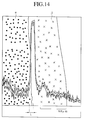
- FIG. 14 shows this result. Referring to FIG. 14, the region ⁇ indicates a pad and the region ⁇ indicates solder. From a result of the linear analysis, it is found that the layer L of 1 ⁇ m containing a large amount of zinc covers the pad.
- the letter A indicates the bonding showing the same as or higher bonding strength than that of ordinary tin-lead solders (about 3.5 kgf/mm 2 ), and the letter B indicates parts inferior to the tin-lead solder or which failed to be bonded.
- bonding strength of the solder differs depending on the ratio of content of zinc in the layer L. Bonding portions which indicated excellent bonding have fewer fine cavities created in the solder than ordinary tin-lead solders. It is considered that this improved the tension strength.
- the layer L composed of mainly zinc forms excellent bonding with gold, silver and copper. Further, even if a member to be bonded is a mixture material composed of mainly gold, silver or copper and other metal, the same excellent bonding can be achieved.
- Table 3 shows a relation between the compositions of the layer L and the hardened tin-zinc solder and bonding strength in a case when the bonding is formed in such a condition that the layer L composed of mainly zinc, exists between a copper member to be bonded and the tin-zinc solder.
- Control of the compositions of the Layer and the hardened tin-zin solder was achieved by changing the composition of the used tin-zinc solder containing 5 to 13 wt% zinc, changing the temperature at which the melted tin-zinc solder was held in the melting bath within a range of 205 to 235 °C, and changing the cooling speed of the solder applied to the copper member.
- the letter A shows the bonding strength being 5 kgf/mm 2 or more
- the letter B shows that of 3.5 to 5.0 kgf/mm 2
- the letter C shows that of being less than 3.5 kgf/mm 2 .
- Zinc Content of Hard Solder Bonding Strength Zinc Content in the Layer L(wt%) 50 88 95 99.5 4.8 C C C C 5.8 C B B B 8.8 C B A A 10 C B A A 11.7 C B B B 12.3 C C C C C
- solder in which, in terms of composition ratio, tin was at least 90.9 wt%, zinc was 9 wt%, oxygen content was at most 5 ppm and other metallic elements content was less than 0.1 wt% was prepared under very low oxygen environment.
- Argon gas was blown into a leveler plating solder bath so as to obtain non-oxidizing environment, in which solder is thrown and melted.
- a substrate having specifications below, provided with the pad is immersed in melted solder. Consequently, a substrate in which leveler plating layer was uniformly formed by solder was obtained.
- the bonding material composed of metallic composition without lead, electronic parts are mounted on a mounting substrate.
- the bonding material can be supplied to fine portions accurately, so that mounting of parts on the high density mounting substrate is facilitated.
- the bonding strength is excellent.
- a mounting substrate having bonded parts likely to have a sufficient strength at bonding portions formed with bonding material, and a sufficient resistance to distortion. Thus, this is advantageous in terms of industry and environmental protection.
Landscapes
- Engineering & Computer Science (AREA)
- Microelectronics & Electronic Packaging (AREA)
- Manufacturing & Machinery (AREA)
- Mechanical Engineering (AREA)
- Electric Connection Of Electric Components To Printed Circuits (AREA)
- Structure Of Printed Boards (AREA)
Applications Claiming Priority (3)
| Application Number | Priority Date | Filing Date | Title |
|---|---|---|---|
| JP108487/97 | 1997-04-25 | ||
| JP10848797A JP3688429B2 (ja) | 1997-04-25 | 1997-04-25 | 電子部品実装用基板および電子部品実装基板 |
| JP10848797 | 1997-04-25 |
Publications (3)
| Publication Number | Publication Date |
|---|---|
| EP0875331A2 true EP0875331A2 (de) | 1998-11-04 |
| EP0875331A3 EP0875331A3 (de) | 1999-04-21 |
| EP0875331B1 EP0875331B1 (de) | 2001-11-21 |
Family
ID=14486016
Family Applications (1)
| Application Number | Title | Priority Date | Filing Date |
|---|---|---|---|
| EP97116635A Expired - Lifetime EP0875331B1 (de) | 1997-04-25 | 1997-09-24 | Verfahren zum Verbinden von einem Substrat und einem elektronischen Bauteil |
Country Status (5)
| Country | Link |
|---|---|
| US (3) | US6280858B1 (de) |
| EP (1) | EP0875331B1 (de) |
| JP (1) | JP3688429B2 (de) |
| CN (1) | CN1110063C (de) |
| DE (1) | DE69709699T2 (de) |
Cited By (8)
| Publication number | Priority date | Publication date | Assignee | Title |
|---|---|---|---|---|
| EP1002612A1 (de) * | 1998-11-20 | 2000-05-24 | Lucent Technologies Inc. | Kinetisch überprüfte Lötverbindung |
| EP1112803A1 (de) * | 1999-12-28 | 2001-07-04 | Kabushiki Kaisha Toshiba | Weichlötmaterial, Vorrichtung welche selbige benutzt und Verfahren zu dieser Herstellung |
| GB2368308A (en) * | 2000-08-18 | 2002-05-01 | Visteon Global Tech Inc | Solder composition |
| EP1295665A3 (de) * | 2001-06-01 | 2004-09-15 | Nec Corporation | Verfahren zum Herstellen von Aufbauzuordnungen ohne Verminderung von Kleberkraft von elektronischen Teilen durch Trennung von niederfesten/niedrig schmelzenden Legierungen |
| EP1307076A4 (de) * | 2000-07-12 | 2005-01-12 | Rohm Co Ltd | Struktur zur verbindung von leitern und verbindungsverfahren |
| US7323359B2 (en) | 2003-07-31 | 2008-01-29 | Infineon Technologies Ag | Mounting method for a semiconductor component |
| EP2891538A4 (de) * | 2012-08-31 | 2016-05-04 | Senju Metal Industry Co | Elektrisch leitfähiges bindematerial |
| US10136520B2 (en) | 2015-09-18 | 2018-11-20 | Quartzdyne, Inc. | Methods of forming a microelectronic device structure, and related microelectronic device structures and microelectronic devices |
Families Citing this family (45)
| Publication number | Priority date | Publication date | Assignee | Title |
|---|---|---|---|---|
| JP3420917B2 (ja) * | 1997-09-08 | 2003-06-30 | 富士通株式会社 | 半導体装置 |
| US20020046627A1 (en) * | 1998-06-10 | 2002-04-25 | Hitoshi Amita | Solder powder, flux, solder paste, soldering method, soldered circuit board, and soldered joint product |
| KR100560235B1 (ko) * | 1999-01-11 | 2006-03-10 | 마쯔시다덴기산교 가부시키가이샤 | 부품실장 회로 형성체 및 이것을 포함하는 전기제품의리사이클 방법 |
| US6782610B1 (en) * | 1999-05-21 | 2004-08-31 | North Corporation | Method for fabricating a wiring substrate by electroplating a wiring film on a metal base |
| JP3580731B2 (ja) * | 1999-06-11 | 2004-10-27 | 和美 松重 | 鉛フリー半田の半田付け方法、及び当該半田付け方法にて半田付けされた接合体 |
| FI108376B (fi) * | 2000-03-21 | 2002-01-15 | Outokumpu Oy | Menetelmõ sõhk÷õjohtavan liitoksen muodostamiseksi |
| KR100387488B1 (ko) * | 2001-04-25 | 2003-06-18 | 현대자동차주식회사 | 레이저 클래딩 공법을 이용한 밸브 시트 제조방법 |
| JP2003037133A (ja) * | 2001-07-25 | 2003-02-07 | Hitachi Ltd | 半導体装置およびその製造方法ならびに電子装置 |
| US7202556B2 (en) * | 2001-12-20 | 2007-04-10 | Micron Technology, Inc. | Semiconductor package having substrate with multi-layer metal bumps |
| JP2003338682A (ja) * | 2002-01-11 | 2003-11-28 | Nec Infrontia Corp | はんだ付け方法及びはんだ接合体 |
| WO2003064102A1 (en) * | 2002-01-30 | 2003-08-07 | Showa Denko K.K. | Solder metal, soldering flux and solder paste |
| US20040075528A1 (en) * | 2002-10-22 | 2004-04-22 | Oak-Mitsui, Inc. | Printed circuit heaters with ultrathin low resistivity materials |
| JP3878978B2 (ja) * | 2002-10-24 | 2007-02-07 | コーア株式会社 | 鉛非含有はんだ、および鉛非含有の継手 |
| JP4112946B2 (ja) * | 2002-10-31 | 2008-07-02 | 株式会社東芝 | 非鉛系接合材、ソルダーペースト及び接合方法 |
| KR100495184B1 (ko) * | 2002-12-02 | 2005-06-14 | 엘지마이크론 주식회사 | 테이프기판 및 그의 주석도금방법 |
| EP1462207A1 (de) * | 2003-03-29 | 2004-09-29 | Grillo-Werke AG | Verfahren zum Schutzgasschweissen oder Schutzgaslöten von Werkstücken gleicher oder verschiedener Metalle oder Metalllegierungen mit einem Zn/Al Zusatzmaterial |
| JP2005026188A (ja) * | 2003-07-03 | 2005-01-27 | Koa Corp | 電流ヒューズ及び電流ヒューズの製造方法 |
| US20050100474A1 (en) * | 2003-11-06 | 2005-05-12 | Benlih Huang | Anti-tombstoning lead free alloys for surface mount reflow soldering |
| US20050121806A1 (en) * | 2003-12-04 | 2005-06-09 | White Electronic Designs Corporation | Method for attaching circuit elements |
| US7167375B2 (en) * | 2004-01-16 | 2007-01-23 | Motorola, Inc. | Populated printed wiring board and method of manufacture |
| JP4141403B2 (ja) * | 2004-04-01 | 2008-08-27 | 富士通株式会社 | 半導体装置及び半導体装置の製造方法 |
| JP4522752B2 (ja) * | 2004-06-10 | 2010-08-11 | 三菱電機株式会社 | 半田付けによる端子接合方法 |
| TW200610122A (en) * | 2004-09-14 | 2006-03-16 | P Kay Metal Inc | Soldering process |
| JP4706825B2 (ja) * | 2005-02-18 | 2011-06-22 | 日亜化学工業株式会社 | サイドビュー型発光装置 |
| JP4570505B2 (ja) * | 2005-02-23 | 2010-10-27 | 古河電気工業株式会社 | 鉛フリー半田付け基板及びその製造方法 |
| EP1749616A1 (de) * | 2005-08-05 | 2007-02-07 | Grillo-Werke AG | Verfahren zum Lichtbogen- oder Strahllöten/-schweissen von Werkstücken gleicher oder verschiedener Metalle oder Metalllegierungen mit Zusatzwerkstoffen aus Sn-Basis-Legierungen; Draht bestehend aus einer Zinn-Basis-Legierung |
| US7749336B2 (en) * | 2005-08-30 | 2010-07-06 | Indium Corporation Of America | Technique for increasing the compliance of tin-indium solders |
| US20070071634A1 (en) * | 2005-09-26 | 2007-03-29 | Indium Corporation Of America | Low melting temperature compliant solders |
| US20100291399A1 (en) * | 2006-09-01 | 2010-11-18 | Rikiya Kato | Lid for a functional part and a process for its manufacture |
| DE102008036837A1 (de) | 2008-08-07 | 2010-02-18 | Epcos Ag | Sensorvorrichtung und Verfahren zur Herstellung |
| US7980302B2 (en) * | 2008-10-13 | 2011-07-19 | Weatherford/Lamb, Inc. | Compliant expansion swage |
| FR2990759B1 (fr) * | 2012-05-21 | 2014-05-02 | Schneider Electric Ind Sas | Capteur de courant mixte et procede de montage dudit capteur |
| CN103913134B (zh) * | 2014-04-30 | 2016-06-01 | 陈姚佳 | 细圆柱工件表面粗糙度的快速检测装置及其检测方法 |
| KR20160010960A (ko) * | 2014-07-21 | 2016-01-29 | 삼성전기주식회사 | 인쇄회로기판 및 그 제조방법 |
| CN104353840B (zh) * | 2014-11-25 | 2017-11-03 | 北京康普锡威科技有限公司 | 一种led用低成本无铅焊料合金粉末及其制备方法 |
| CN105448744B (zh) * | 2015-11-17 | 2017-11-07 | 通富微电子股份有限公司 | 无助焊剂式凸块回流成球率控制方法 |
| WO2017221425A1 (ja) * | 2016-06-24 | 2017-12-28 | 朝日インテック株式会社 | ガイドワイヤ |
| DE102016216308B4 (de) * | 2016-08-30 | 2022-06-15 | Schweizer Electronic Ag | Leiterplatte und Verfahren zu deren Herstellung |
| JP7247860B2 (ja) * | 2019-10-25 | 2023-03-29 | 株式会社村田製作所 | インダクタ部品 |
| JP7243569B2 (ja) * | 2019-10-25 | 2023-03-22 | 株式会社村田製作所 | インダクタ部品およびインダクタ部品内蔵基板 |
| JP7698943B2 (ja) * | 2020-02-29 | 2025-06-26 | 太陽誘電株式会社 | コイル部品、回路基板及び電子機器 |
| JP7503401B2 (ja) * | 2020-03-19 | 2024-06-20 | 太陽誘電株式会社 | コイル部品及び電子機器 |
| JP7294300B2 (ja) * | 2020-10-28 | 2023-06-20 | 株式会社村田製作所 | インダクタ部品及びインダクタ部品実装基板 |
| CN116615962A (zh) | 2020-12-17 | 2023-08-18 | 特斯拉公司 | 堆叠式器件阵列结构 |
| US12341126B2 (en) * | 2022-04-27 | 2025-06-24 | Texas Instruments Incorporated | Bump to package substrate solder joint |
Family Cites Families (25)
| Publication number | Priority date | Publication date | Assignee | Title |
|---|---|---|---|---|
| US1233803A (en) * | 1916-04-24 | 1917-07-17 | Overend Aluminium Soldering Processes Ltd | Soldering of aluminium or aluminium alloys. |
| US1437641A (en) | 1919-09-11 | 1922-12-05 | Pfyffer | Solder for aluminum and its alloys |
| US3698475A (en) | 1966-01-28 | 1972-10-17 | Stolle Corp | Flat sheet of metal having an elongated member secured thereto |
| US3685487A (en) | 1969-10-24 | 1972-08-22 | Dynamics Corp America | Coating trough with sonic energy activating means |
| US4386051A (en) * | 1980-09-19 | 1983-05-31 | Edgington Robert E | Tin, lead, zinc alloy |
| US4670217A (en) | 1985-07-26 | 1987-06-02 | J. W. Harris Company | Solder composition |
| FR2589379B1 (fr) * | 1985-11-05 | 1990-09-21 | Asturienne France | Composition de soudure ou de brasure, notamment pour l'assemblage d'elements de zinc |
| US4695428A (en) | 1986-08-21 | 1987-09-22 | J. W. Harris Company | Solder composition |
| EP0412259B1 (de) * | 1989-06-16 | 1995-09-27 | Matsushita Electric Industrial Co., Ltd. | Elektronische Verbindungen, Verfahren zur Bildung von Endverbindern dafür und Paste zur Ausbildung derselben |
| US5242658A (en) * | 1992-07-07 | 1993-09-07 | The Indium Corporation Of America | Lead-free alloy containing tin, zinc and indium |
| EP0612578A1 (de) | 1993-02-22 | 1994-08-31 | AT&T Corp. | Gegenstand, der ein bleifreies Weichlot mit verbesserten mechanischen Eigenschaften enthält |
| TW251249B (de) * | 1993-04-30 | 1995-07-11 | At & T Corp | |
| US5390080A (en) * | 1993-05-03 | 1995-02-14 | Motorola | Tin-zinc solder connection to a printed circuit board of the like |
| US5705261A (en) * | 1993-10-28 | 1998-01-06 | Saint-Gobain/Norton Industrial Ceramics Corporation | Active metal metallization of mini-igniters by silk screening |
| DE69524912T2 (de) | 1994-09-30 | 2002-08-22 | AT & T CORP., NEW YORK | Bleifreie Legierungen zum Weichlöten |
| JP3232963B2 (ja) * | 1994-10-11 | 2001-11-26 | 株式会社日立製作所 | 有機基板接続用鉛レスはんだ及びそれを用いた実装品 |
| JPH08243782A (ja) * | 1995-03-08 | 1996-09-24 | Toshiba Corp | はんだ合金およびそれを用いたはんだ付け方法 |
| JPH0970687A (ja) * | 1995-07-04 | 1997-03-18 | Toyota Central Res & Dev Lab Inc | 無鉛はんだ合金 |
| JP3550233B2 (ja) * | 1995-10-09 | 2004-08-04 | 同和鉱業株式会社 | 高強度高導電性銅基合金の製造法 |
| WO1997047426A1 (en) * | 1996-06-12 | 1997-12-18 | International Business Machines Corporation | Lead-free, high tin ternary solder alloy of tin, silver, and indium |
| JP3493101B2 (ja) * | 1996-08-15 | 2004-02-03 | 三井金属鉱業株式会社 | 半田粉及びその製造方法、及びその半田粉を用いた半田ペースト |
| US5863493A (en) * | 1996-12-16 | 1999-01-26 | Ford Motor Company | Lead-free solder compositions |
| JPH10328880A (ja) * | 1997-06-04 | 1998-12-15 | Mitsui Mining & Smelting Co Ltd | 錫−銀系無鉛半田合金 |
| JP3311282B2 (ja) * | 1997-10-13 | 2002-08-05 | 株式会社東芝 | 金属部材の接合方法及び接合体 |
| JP3335896B2 (ja) * | 1997-12-26 | 2002-10-21 | 株式会社東芝 | ハンダ材及びハンダ材の製造方法 |
-
1997
- 1997-04-25 JP JP10848797A patent/JP3688429B2/ja not_active Expired - Fee Related
- 1997-09-24 DE DE69709699T patent/DE69709699T2/de not_active Expired - Fee Related
- 1997-09-24 EP EP97116635A patent/EP0875331B1/de not_active Expired - Lifetime
- 1997-12-31 CN CN97129783A patent/CN1110063C/zh not_active Expired - Lifetime
-
2000
- 2000-07-19 US US09/619,470 patent/US6280858B1/en not_active Expired - Lifetime
- 2000-07-19 US US09/619,445 patent/US6457632B1/en not_active Expired - Lifetime
-
2002
- 2002-08-08 US US10/214,187 patent/US6651870B2/en not_active Expired - Lifetime
Cited By (14)
| Publication number | Priority date | Publication date | Assignee | Title |
|---|---|---|---|---|
| US6342442B1 (en) | 1998-11-20 | 2002-01-29 | Agere Systems Guardian Corp. | Kinetically controlled solder bonding |
| EP1002612A1 (de) * | 1998-11-20 | 2000-05-24 | Lucent Technologies Inc. | Kinetisch überprüfte Lötverbindung |
| EP1112803A1 (de) * | 1999-12-28 | 2001-07-04 | Kabushiki Kaisha Toshiba | Weichlötmaterial, Vorrichtung welche selbige benutzt und Verfahren zu dieser Herstellung |
| EP1307076A4 (de) * | 2000-07-12 | 2005-01-12 | Rohm Co Ltd | Struktur zur verbindung von leitern und verbindungsverfahren |
| US7018721B2 (en) | 2000-07-12 | 2006-03-28 | Rohm Co., Ltd. | Structure for interconnecting conductors and connecting method |
| GB2368308A (en) * | 2000-08-18 | 2002-05-01 | Visteon Global Tech Inc | Solder composition |
| GB2368308B (en) * | 2000-08-18 | 2004-03-10 | Visteon Global Tech Inc | Method of making a solder composition |
| US6416597B1 (en) | 2000-08-18 | 2002-07-09 | Visteon Global Tech., Inc. | Solder composition and a method for making the same |
| EP1295665A3 (de) * | 2001-06-01 | 2004-09-15 | Nec Corporation | Verfahren zum Herstellen von Aufbauzuordnungen ohne Verminderung von Kleberkraft von elektronischen Teilen durch Trennung von niederfesten/niedrig schmelzenden Legierungen |
| US6915942B2 (en) | 2001-06-01 | 2005-07-12 | Nec Corporation | Method of manufacturing mount structure without introducing degraded bonding strength of electronic parts due to segregation of low-strength/low-melting point alloy |
| US7323359B2 (en) | 2003-07-31 | 2008-01-29 | Infineon Technologies Ag | Mounting method for a semiconductor component |
| EP2891538A4 (de) * | 2012-08-31 | 2016-05-04 | Senju Metal Industry Co | Elektrisch leitfähiges bindematerial |
| US9487846B2 (en) | 2012-08-31 | 2016-11-08 | Senju Metal Industry Co., Ltd. | Electroconductive bonding material |
| US10136520B2 (en) | 2015-09-18 | 2018-11-20 | Quartzdyne, Inc. | Methods of forming a microelectronic device structure, and related microelectronic device structures and microelectronic devices |
Also Published As
| Publication number | Publication date |
|---|---|
| US6280858B1 (en) | 2001-08-28 |
| US6457632B1 (en) | 2002-10-01 |
| EP0875331B1 (de) | 2001-11-21 |
| DE69709699T2 (de) | 2002-08-08 |
| US6651870B2 (en) | 2003-11-25 |
| CN1197996A (zh) | 1998-11-04 |
| US20030015574A1 (en) | 2003-01-23 |
| CN1110063C (zh) | 2003-05-28 |
| EP0875331A3 (de) | 1999-04-21 |
| JP3688429B2 (ja) | 2005-08-31 |
| JPH10303518A (ja) | 1998-11-13 |
| DE69709699D1 (de) | 2002-02-21 |
Similar Documents
| Publication | Publication Date | Title |
|---|---|---|
| US6457632B1 (en) | Solder alloy and bonding method of substrate and electric or electronic parts with solder alloy | |
| US6464122B1 (en) | Soldering method and soldering apparatus | |
| US6220501B1 (en) | Method of joining metallic members, and joined metallic members | |
| CN1301049C (zh) | 锡焊方法及焊接结构体 | |
| Pecht | Soldering processes and equipment | |
| US9289841B2 (en) | Soldering device, soldering method, and substrate and electronic component produced by the soldering device or the soldering method | |
| US5071058A (en) | Process for joining/coating using an atmosphere having a controlled oxidation capability | |
| KR100671394B1 (ko) | Pb프리 땜납 합금을 이용한 리플로우 납땜 방법 및 혼재실장 방법 및 혼재 실장 구조체 | |
| EP2671661B1 (de) | Lötvorrichtung und -verfahren sowie damit hergestelltes substrat und elektronische komponente | |
| WO2007055410A1 (en) | Method for soldering electronic component and soldering structure of electronic component | |
| Artaki et al. | Wave soldering with Pb-free solders | |
| KR100808746B1 (ko) | 회로 장치의 제조 방법 | |
| JP4112946B2 (ja) | 非鉛系接合材、ソルダーペースト及び接合方法 | |
| KR940001030B1 (ko) | 조절된 산화능력을 갖는 대기를 사용하는 결합/피복방법 | |
| JPH1197839A (ja) | 電子部品実装用基板、電子部品実装基板及び実装方法並びに基板の被接合部材 | |
| JP3801893B2 (ja) | 部材の接合方法 | |
| JP3460442B2 (ja) | 鉛フリーはんだ及びそれを用いた実装品 | |
| JP3392778B2 (ja) | 非鉛系接合部材の形成方法、及び回路基板 | |
| HK40097099A (zh) | 凸点电极基板的形成方法 | |
| Primavera | Electronics Assembly and the Impact of Lead-Free Materials | |
| JP2007096125A (ja) | はんだ接合方法、及び、これによって製造した実装回路基板 | |
| HK1099469B (en) | Soldering method and solder joint member |
Legal Events
| Date | Code | Title | Description |
|---|---|---|---|
| PUAI | Public reference made under article 153(3) epc to a published international application that has entered the european phase |
Free format text: ORIGINAL CODE: 0009012 |
|
| 17P | Request for examination filed |
Effective date: 19970924 |
|
| AK | Designated contracting states |
Kind code of ref document: A2 Designated state(s): DE FR GB |
|
| PUAL | Search report despatched |
Free format text: ORIGINAL CODE: 0009013 |
|
| AK | Designated contracting states |
Kind code of ref document: A3 Designated state(s): AT BE CH DE DK ES FI FR GB GR IE IT LI LU MC NL PT SE |
|
| 17Q | First examination report despatched |
Effective date: 19990917 |
|
| AKX | Designation fees paid |
Free format text: DE FR GB |
|
| GRAG | Despatch of communication of intention to grant |
Free format text: ORIGINAL CODE: EPIDOS AGRA |
|
| RTI1 | Title (correction) |
Free format text: METHOD OF BONDING AN ELECTRONIC PART TO A SUBSTRATE. |
|
| GRAG | Despatch of communication of intention to grant |
Free format text: ORIGINAL CODE: EPIDOS AGRA |
|
| GRAG | Despatch of communication of intention to grant |
Free format text: ORIGINAL CODE: EPIDOS AGRA |
|
| GRAH | Despatch of communication of intention to grant a patent |
Free format text: ORIGINAL CODE: EPIDOS IGRA |
|
| GRAH | Despatch of communication of intention to grant a patent |
Free format text: ORIGINAL CODE: EPIDOS IGRA |
|
| GRAA | (expected) grant |
Free format text: ORIGINAL CODE: 0009210 |
|
| AK | Designated contracting states |
Kind code of ref document: B1 Designated state(s): DE FR GB |
|
| REG | Reference to a national code |
Ref country code: GB Ref legal event code: IF02 |
|
| REF | Corresponds to: |
Ref document number: 69709699 Country of ref document: DE Date of ref document: 20020221 |
|
| ET | Fr: translation filed | ||
| PLBE | No opposition filed within time limit |
Free format text: ORIGINAL CODE: 0009261 |
|
| STAA | Information on the status of an ep patent application or granted ep patent |
Free format text: STATUS: NO OPPOSITION FILED WITHIN TIME LIMIT |
|
| 26N | No opposition filed | ||
| PGFP | Annual fee paid to national office [announced via postgrant information from national office to epo] |
Ref country code: DE Payment date: 20081002 Year of fee payment: 12 |
|
| PG25 | Lapsed in a contracting state [announced via postgrant information from national office to epo] |
Ref country code: DE Free format text: LAPSE BECAUSE OF NON-PAYMENT OF DUE FEES Effective date: 20100401 |
|
| REG | Reference to a national code |
Ref country code: FR Ref legal event code: PLFP Year of fee payment: 20 |
|
| PGFP | Annual fee paid to national office [announced via postgrant information from national office to epo] |
Ref country code: GB Payment date: 20160921 Year of fee payment: 20 |
|
| PGFP | Annual fee paid to national office [announced via postgrant information from national office to epo] |
Ref country code: FR Payment date: 20160816 Year of fee payment: 20 |
|
| REG | Reference to a national code |
Ref country code: GB Ref legal event code: PE20 Expiry date: 20170923 |
|
| PG25 | Lapsed in a contracting state [announced via postgrant information from national office to epo] |
Ref country code: GB Free format text: LAPSE BECAUSE OF EXPIRATION OF PROTECTION Effective date: 20170923 |