EP0875937A2 - Réseau de cellules DRAM et son procédé de fabrication - Google Patents
Réseau de cellules DRAM et son procédé de fabrication Download PDFInfo
- Publication number
- EP0875937A2 EP0875937A2 EP98106069A EP98106069A EP0875937A2 EP 0875937 A2 EP0875937 A2 EP 0875937A2 EP 98106069 A EP98106069 A EP 98106069A EP 98106069 A EP98106069 A EP 98106069A EP 0875937 A2 EP0875937 A2 EP 0875937A2
- Authority
- EP
- European Patent Office
- Prior art keywords
- trenches
- layer
- gate electrode
- source
- mos transistor
- Prior art date
- Legal status (The legal status is an assumption and is not a legal conclusion. Google has not performed a legal analysis and makes no representation as to the accuracy of the status listed.)
- Withdrawn
Links
Images




Classifications
-
- H—ELECTRICITY
- H10—SEMICONDUCTOR DEVICES; ELECTRIC SOLID-STATE DEVICES NOT OTHERWISE PROVIDED FOR
- H10B—ELECTRONIC MEMORY DEVICES
- H10B12/00—Dynamic random access memory [DRAM] devices
- H10B12/01—Manufacture or treatment
- H10B12/02—Manufacture or treatment for one transistor one-capacitor [1T-1C] memory cells
- H10B12/03—Making the capacitor or connections thereto
- H10B12/038—Making the capacitor or connections thereto the capacitor being in a trench in the substrate
- H10B12/0383—Making the capacitor or connections thereto the capacitor being in a trench in the substrate wherein the transistor is vertical
-
- H—ELECTRICITY
- H10—SEMICONDUCTOR DEVICES; ELECTRIC SOLID-STATE DEVICES NOT OTHERWISE PROVIDED FOR
- H10B—ELECTRONIC MEMORY DEVICES
- H10B12/00—Dynamic random access memory [DRAM] devices
- H10B12/30—DRAM devices comprising one-transistor - one-capacitor [1T-1C] memory cells
- H10B12/39—DRAM devices comprising one-transistor - one-capacitor [1T-1C] memory cells the capacitor and the transistor being in a same trench
- H10B12/395—DRAM devices comprising one-transistor - one-capacitor [1T-1C] memory cells the capacitor and the transistor being in a same trench the transistor being vertical
Definitions
- a single transistor memory cell includes a read transistor and a storage capacitor.
- the Information stored in the form of an electrical charge which is a logical quantity, 0 or 1.
- the required area of the single-transistor memory cell be reduced from generation to generation. Since the reduction of the structure sizes by the minimal in the structure size F limits that can be produced in each technology are set, this is also with a change in the single-transistor memory cell connected. So were up to the 1MBit generation both the readout transistor and the storage capacitor realized as planar components. From the 4MBit memory generation had to further reduce the area through a three-dimensional arrangement of the read transistor and storage capacitor.
- each vertical MOS transistor comprises two opposite edges of a trench, along which a bit line runs. Doped regions are provided in the upper region of the flanks, which act as the drain region of the MOS transistors.
- the surface of the flanks is provided with gate oxide.
- a gate electrode is provided which covers the opposite surfaces of the gate oxide.
- the gate electrode is insulated from the buried bit line arranged below it and from a storage node arranged above it by an insulating layer.
- Shallow trenches are provided in the surface of the substrate, which run transversely to the bit lines and in which word lines run transversely to the bit lines.
- the word lines are laterally adjacent to the gate electrode and are thus connected to it.
- the smallest area of a memory cell that can be achieved with this method is 6 F 2 .
- a DRAM arrangement is known in which Trenches are provided in a semiconductor substrate.
- a Drainage area is provided at the bottom of the trench.
- At the A source region is provided on the surface of the substrate.
- the side walls of the trench are with gate oxide and gate electrode provide and act as a channel area.
- the gate electrodes are embedded in an insulation layer in which a contact hole down to the surface of the bottom of the trench Drainage area is sufficient and provided with an electrode is.
- the trench is on the side of the surface of the semiconductor substrate a capacitor is provided.
- the lateral arrangement of capacitor and transistor means an increased Space requirement of the memory cell.
- a read-out transistor has a first source / drain region which surrounds a gate electrode in a ring and is part of a bit line.
- a second source / drain region of the read-out transistor is produced by out-diffusion of dopant from a storage node which is implemented in a recess and is arranged below the gate electrode.
- Word lines which partly consist of gate electrodes, run over the bit lines.
- the read-out transistor comprises flanks of the gate electrode parallel to at least the bit lines. The area of a memory cell 9 F 2 .
- a DRAM cell arrangement which comprises a vertical MOS transistor per memory cell, the first source / drain region of which is connected to a storage node of a storage capacitor, the channel region of which is surrounded by a gate electrode and the second of which Source-drain region is connected to a buried bit line.
- the storage capacitor is either a planar capacitor or a stacked capacitor.
- the DRAM cell arrangement can be produced with a memory cell area of 4 F 2 .
- the area of a memory cell of a 1 GBit DRAM generation should only be approximately 0.2 ⁇ m 2 .
- the storage capacitor must have a capacitance of 20 to 30fF.
- the invention is based on the problem of a DRAM cell arrangement specify the memory cells as single-transistor cells includes and in the for the 1GBit generation required packing density can be produced. Further is a manufacturing method for such a DRAM cell arrangement can be specified.
- the read transistor is designed as a vertical MOS transistor.
- everybody MOS transistor comprises two opposite, parallel to Flanks running word line and adjacent to a gate oxide a gate electrode.
- the MOS transistor has exactly two first source / drain regions that are spatially separated along a bit line via which they are connected are. Every first source / drain region belongs to two along transistors adjacent to the bit line, resulting in a leads to small cell area.
- the cell area can be reduced in size since no adjustment tolerances have to be taken into account.
- the storage nodes are self-aligned under the word lines and isolated from adjacent storage nodes.
- the contacts of the first source / drain regions to the bit lines are opened in a self-aligned manner. This allows the production of 4F 2 cell areas with only 3 masks.
- Second source / drain regions of the MOS transistor are with a Storage nodes connected. They are preferred by diffusion of dopant from the storage node into a suitable one structured layer. This will make the Storage nodes self-aligned with the second source / drain regions connected and the cell area is kept small.
- the junction depth i.e. the distance of minimum distance between source and drain perpendicular to the current flow and perpendicular to the gate electrode, is kept small, which means short channel effects, like punch through, positively influenced.
- gate electrode as part the word line to train what the number of process steps required reduced, as well as a self-aligned connection between gate electrode and word line.
- the Apply a layer of silicon nitride to the substrate In order not to etch too deeply when opening the contacts of the first source / drain regions to the bit lines SiO 2 according to one embodiment, which can lead to a short circuit between the word lines and the bit lines, it is advantageous at the beginning of the DRAM production that the Apply a layer of silicon nitride to the substrate.
- the exposure of the silicon nitride layer by changing physical conditions, such as the gas composition provides an end point signal for the etching.
- it is advantageous to apply a thin SiO 2 layer before producing the silicon nitride layer In order to avoid surface damage to the substrate by silicon nitride, it is advantageous to apply a thin SiO 2 layer before producing the silicon nitride layer.
- the starting material is a substrate made of, for example, monocrystalline silicon, which is doped in a region B of a first conductivity type.
- Area B has, for example, p-type doping with a dopant concentration of approximately 3 * 10 16 cm -3 and is provided with a first layer 1 that is of a second conductivity type opposite to the first conductivity type with a dopant concentration of approximately 10 20 cm -3 is doped with a second layer 2, which is doped of the first conductivity type with a dopant concentration of approx. 3 * 10 17 cm -3 , and a third layer 3, which is of the second conductivity type with a dopant concentration of approx. 10 21 cm -3 is doped, provided (see Fig. 1).
- the first layer 1, the second layer 2 and the third layer 3 are produced, for example, by epitaxial growth.
- the third layer 3 forms a surface 4 of the substrate.
- the first layer 1 has a thickness of approximately 9 ⁇ m
- the second layer 2 has a thickness of approximately 1 ⁇ m
- the third layer 3 has a thickness of approximately 200 nm.
- a first approximately 150 nm thick SiO 2 layer O1 is deposited on the surface 4 in a TEOS process (see FIG. 1).
- the first SiO 2 layer O1 is structured with the aid of a first photoresist mask (not shown), parts of the surface 4 being exposed in order to be able to produce first trenches G1.
- the first trenches G1 are etched selectively to SiO 2 in an anisotropic drying process (see FIG. 2). HBr, NF 3 , He, O 2 , for example, are suitable as the etching process in which silicon is attacked selectively to SiO 2 .
- the first trenches G1 are produced with a depth of approximately 800 nm and extend into the second layer 2. Parallel to the surface 4, the first trenches G1 have a strip-shaped cross section and run essentially parallel over the entire cell field.
- the first trenches G1 have a width of approx. 200 nm and a length of approx. 50 ⁇ m.
- the first trenches G1 are filled by depositing a second SiO 2 layer O2, for example 150 nm thick, in a TEOS process.
- the surface 4 is covered by parts of the first SiO 2 layer O1 and by parts of the second SiO 2 layer O2, ie with a total of 300 nm SiO 2 (see FIG. 4).
- SiO 2 is selectively converted to silicon by means of anisotropic dry etching to a second depth T2, which is above an interface between the first layer 1 and the second layer 2 and below an interface between the second layer 2, using a second photoresist mask and the third layer 3 lies and is approximately 400 nm from the surface 4, etched (see FIG. 3). Parts of the surface 4 which are not attacked because of the selectivity of the etching are thereby exposed (see FIG. 4).
- CHF 3 , CF 4 , and / or Ar is suitable as the etching process in which SiO 2 is attacked selectively to silicon. Silicon is then selectively etched to SiO 2 to a first depth T1 within the first layer 1.
- the first depth T1 is, for example, 10 ⁇ m below the surface 4.
- the second trenches G2 produced are, for example, perpendicular to the first trenches G1 (see FIG. 5).
- the second trenches G2 have a width of approximately 200 nm and a length of approximately 50 ⁇ m.
- the distance between the centers of adjacent second trenches G2 is approximately 400 nm.
- the first trenches G1 and the second trenches G2, which are partially filled with SiO 2 intersect in intersection areas K.
- the second trenches G2 have the second depth T2 in the intersection areas K (see FIG. 3). In areas between the intersection areas K. K the second trenches G2 have the first depth T1 (see FIG. 5).
- the second trenches G2 have a strip-shaped cross section and run essentially parallel. Remaining parts of the third layer 3, which are delimited by the first trenches G1 and the second trenches G2, are suitable as first source / drain regions S / D1.
- a first insulation structure I1 is produced by thermal oxidation of the surfaces of semiconductor material adjoining the second trenches G2 (see FIG. 5).
- the second trenches G2 are then filled by depositing semiconductor material which is doped of the second conductivity type with a dopant concentration of approximately 10 21 cm -3 .
- the thickness of the applied semiconductor material is approx. 200nm.
- silicon is selectively etched to SiO 2 , so that the second trenches G2 in the regions lying between the crossing regions K.
- K are filled with semiconductor material up to a first height H1.
- the first height H1 is located above an interface between the first 1 and second layer 2 and below the second depth T2.
- the first height H1 is approximately 600 nm below the surface 4.
- Parts of the first insulation structure I1 which are exposed in this way are removed by a wet etching process using HF. Remaining parts of the first insulation structure I1 are suitable as capacitor dielectrics Kd (see FIG. 6).
- the second trenches G2 are then filled by depositing semiconductor material which is doped of the second conductivity type with a dopant concentration of approximately 10 21 cm -3 .
- the thickness of the deposited semiconductor material is approximately 200 nm.
- silicon is selectively etched to SiO 2 , so that the second trenches G2 in the regions lying between the crossing regions K. K are filled with semiconductor material up to a second height H2, which lies above the first height H1 and below the second depth T2.
- the second height H2 is approx. 100 nm above the first height H1.
- the semiconductor material up to the second height H2 in the areas lying between the intersection areas K. K the second trenches G2 are suitable as storage nodes SP.
- the storage nodes SP accordingly extend from the second layer 2 to the first layer 1.
- An RTP process diffuses dopant from the storage nodes into the second layer 2. This creates from second conductivity type doped areas are suitable as second source / drain regions S / D2.
- a gate oxide I2 is generated within the second trenches G2 by, for example, thermal oxidation.
- conductive material which contains, for example, polysilicon and / or metal silicide, is deposited in order to fill the second trenches G2.
- the thickness of the deposited conductive material is approximately 200nm.
- the conductive material is etched selectively with respect to SiO 2 , so that the second trenches G2 in the regions lying between the crossing regions K. K up to a third height H3, which lies above the interface between the second 2 and third layer 3 and below the surface 4, are filled with conductive material (see FIG. 7).
- the third height H3 is approx. 150 nm below the surface 4.
- the deposited conductive material forms word lines W1, which lie in the areas lying between the crossing areas K. K are suitable as gate electrodes G.
- the gate electrodes G are thus produced in a self-aligned manner via the storage node Sp.
- the second trenches G2 are filled by depositing SiO 2 in a TEOS process.
- the thickness of the deposited SiO 2 is approximately 200 nm.
- SiO 2 is then selectively etched to silicon until the surface 4 is exposed. This step completely removes the first SiO 2 layer O1 and the second SiO 2 layer O2. Since only the first source / drain regions S / D1 and insulating materials adjoin a section along the surface 4, contacts to the first source / drain regions S / D1 are thereby opened in a self-aligned manner.
- bit lines BL are produced by depositing and structuring conductive material.
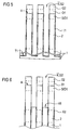
- the bit lines B1 are arranged such that they overlap the first source / drain regions S / D1 (see FIGS. 8 and 9).
- the conductive material contains, for example, polysilicon, metal silicide and / or tungsten.
- Each MOS transistor consists of a gate electrode G, which is part of a word line W1, two first source / drain regions S / D1, which were created by structuring the third layer 3 and which overlap with a bit line B1, two perpendicular to the surface 4 Channel areas, which are located within the second layer 2 and to which a gate oxide is adjacent, and two second source / drain regions S / D2, which resulted from the diffusion of dopant from a storage node Sp into the second layer 2 and which are connected to the storage node Sp are connected (see FIG. 8).
- SiO 2 in the first trenches G1 insulates adjacent transistors from one another in the word line direction, and word lines W1 from bit lines B1.
- the storage nodes Sp are arranged below the gate electrodes G.
- a layer can be formed on the surface 4, which consists of, for example, three partial layers, of which a middle, approximately 80 nm thick, partial layer contains silicon nitride.
- a lower, approximately 20 nm thick partial layer made of SiO 2 which is intended to prevent surface damage to the substrate by silicon nitride, is produced by thermal oxidation.
- An upper approximately 50 nm thick partial layer made of SiO 2 is produced, for example, in a TEOS process. In each etching process that exposes parts of the surface 4, not only SiO 2 but also silicon nitride must be etched with it. This alternative reduces the risk of the etching of the contacts of the first source / drain regions S / D1 being too deep, which would lead to a short circuit between word lines W1 and bit lines B1 (see FIG. 9).
Landscapes
- Engineering & Computer Science (AREA)
- Manufacturing & Machinery (AREA)
- Semiconductor Memories (AREA)
Applications Claiming Priority (2)
| Application Number | Priority Date | Filing Date | Title |
|---|---|---|---|
| DE19718721A DE19718721C2 (de) | 1997-05-02 | 1997-05-02 | DRAM-Zellenanordnung und Verfahren zu deren Herstellung |
| DE19718721 | 1997-05-02 |
Publications (2)
| Publication Number | Publication Date |
|---|---|
| EP0875937A2 true EP0875937A2 (fr) | 1998-11-04 |
| EP0875937A3 EP0875937A3 (fr) | 2003-08-27 |
Family
ID=7828530
Family Applications (1)
| Application Number | Title | Priority Date | Filing Date |
|---|---|---|---|
| EP98106069A Withdrawn EP0875937A3 (fr) | 1997-05-02 | 1998-04-02 | Réseau de cellules DRAM et son procédé de fabrication |
Country Status (6)
| Country | Link |
|---|---|
| US (2) | US6255684B1 (fr) |
| EP (1) | EP0875937A3 (fr) |
| JP (1) | JPH10313100A (fr) |
| KR (1) | KR100509210B1 (fr) |
| DE (1) | DE19718721C2 (fr) |
| TW (1) | TW411622B (fr) |
Cited By (2)
| Publication number | Priority date | Publication date | Assignee | Title |
|---|---|---|---|---|
| WO2002029889A3 (fr) * | 2000-09-29 | 2003-05-22 | Infineon Technologies Corp | Circuit integre a tranchee auto-alignee et son procede de realisation |
| DE10257873B3 (de) * | 2002-12-11 | 2004-06-17 | Infineon Technologies Ag | Dynamische Speicherzelle und Verfahren zur Herstellung derselben |
Families Citing this family (22)
| Publication number | Priority date | Publication date | Assignee | Title |
|---|---|---|---|---|
| AU3895299A (en) * | 1998-05-12 | 1999-11-29 | Wen Y Chen | Use of anti-prolactin agents to treat proliferative conditions |
| DE19845004C2 (de) * | 1998-09-30 | 2002-06-13 | Infineon Technologies Ag | DRAM-Zellenanordnung und Verfahren zu deren Herstellung |
| JP3376302B2 (ja) * | 1998-12-04 | 2003-02-10 | 株式会社東芝 | 半導体装置及びその製造方法 |
| US6383871B1 (en) * | 1999-08-31 | 2002-05-07 | Micron Technology, Inc. | Method of forming multiple oxide thicknesses for merged memory and logic applications |
| US6245615B1 (en) * | 1999-08-31 | 2001-06-12 | Micron Technology, Inc. | Method and apparatus on (110) surfaces of silicon structures with conduction in the <110> direction |
| DE10008814B4 (de) * | 2000-02-25 | 2006-06-29 | Mosel Vitelic Inc. | Aufbau eines Drams mit vertikalem Transistor und dessen Herstellung |
| DE10125967C1 (de) * | 2001-05-29 | 2002-07-11 | Infineon Technologies Ag | DRAM-Zellanordnung mit vertikalen MOS-Transistoren und Verfahren zu deren Herstellung |
| DE10134101B4 (de) * | 2001-07-13 | 2006-03-23 | Infineon Technologies Ag | Integrierter Halbleiterspeicher und Herstellungsverfahren |
| DE10162578A1 (de) * | 2001-12-19 | 2003-08-21 | Infineon Technologies Ag | Schicht-Anordnung, Speicherzelle, Speicherzellen-Anordnung und Verfahren zum Herstellen einer Schicht-Anordnung |
| US6909152B2 (en) * | 2002-11-14 | 2005-06-21 | Infineon Technologies, Ag | High density DRAM with reduced peripheral device area and method of manufacture |
| US6724031B1 (en) * | 2003-01-13 | 2004-04-20 | International Business Machines Corporation | Method for preventing strap-to-strap punch through in vertical DRAMs |
| DE10362018B4 (de) * | 2003-02-14 | 2007-03-08 | Infineon Technologies Ag | Anordnung und Verfahren zur Herstellung von vertikalen Transistorzellen und transistorgesteuerten Speicherzellen |
| US20050088895A1 (en) * | 2003-07-25 | 2005-04-28 | Infineon Technologies Ag | DRAM cell array having vertical memory cells and methods for fabricating a DRAM cell array and a DRAM |
| DE102004026000A1 (de) * | 2003-07-25 | 2005-02-24 | Infineon Technologies Ag | DRAM-Zellenfeld und Halbleiterspeichereinrichtung mit vertikalen Speicherzellen und Verfahren zur Herstellung eines DRAM-Zellenfeldes und eines DRAMs |
| DE10334113A1 (de) * | 2003-07-25 | 2005-03-03 | Infineon Technologies Ag | Anordnung und Verfahren zur Herstellung von vertikalen Speicherzellen für DRAMs in einem Halbleitersubstrat |
| US7135731B2 (en) * | 2003-12-10 | 2006-11-14 | Nanya Technology Corp. | Vertical DRAM and fabrication method thereof |
| WO2007027169A2 (fr) * | 2005-08-30 | 2007-03-08 | University Of South Florida | Procede de fabrication de condensateurs topologiques de silicium |
| JP5623005B2 (ja) | 2008-02-01 | 2014-11-12 | ピーエスフォー ルクスコ エスエイアールエルPS4 Luxco S.a.r.l. | 半導体装置及びその製造方法 |
| US9117701B2 (en) * | 2011-05-06 | 2015-08-25 | Semiconductor Energy Laboratory Co., Ltd. | Semiconductor device |
| US8609492B2 (en) | 2011-07-27 | 2013-12-17 | Micron Technology, Inc. | Vertical memory cell |
| KR102222955B1 (ko) * | 2017-06-26 | 2021-03-05 | 마이크론 테크놀로지, 인크 | 액세스 디바이스와 결합된 바디 연결 라인을 가진 장치 |
| WO2025079920A1 (fr) * | 2023-10-10 | 2025-04-17 | 한양대학교 산학협력단 | Mémoire vive tridimensionnelle à structure améliorée |
Family Cites Families (16)
| Publication number | Priority date | Publication date | Assignee | Title |
|---|---|---|---|---|
| US4824793A (en) * | 1984-09-27 | 1989-04-25 | Texas Instruments Incorporated | Method of making DRAM cell with trench capacitor |
| US4797373A (en) * | 1984-10-31 | 1989-01-10 | Texas Instruments Incorporated | Method of making dRAM cell with trench capacitor |
| US4914739A (en) * | 1984-10-31 | 1990-04-03 | Texas Instruments, Incorporated | Structure for contacting devices in three dimensional circuitry |
| JPH0824165B2 (ja) * | 1985-11-22 | 1996-03-06 | テキサス インスツルメンツ インコ−ポレイテツド | 集積回路 |
| JPS63211750A (ja) * | 1987-02-27 | 1988-09-02 | Mitsubishi Electric Corp | 半導体記憶装置 |
| JPH01227468A (ja) * | 1988-03-08 | 1989-09-11 | Oki Electric Ind Co Ltd | 半導体記憶装置 |
| US5103276A (en) * | 1988-06-01 | 1992-04-07 | Texas Instruments Incorporated | High performance composed pillar dram cell |
| US5218218A (en) * | 1990-02-01 | 1993-06-08 | Mitsubishi Denki Kabushiki Kaisha | Semiconductor device and manufacturing method thereof |
| KR940006679B1 (ko) | 1991-09-26 | 1994-07-25 | 현대전자산업 주식회사 | 수직형 트랜지스터를 갖는 dram셀 및 그 제조방법 |
| JP3322936B2 (ja) * | 1992-03-19 | 2002-09-09 | 株式会社東芝 | 半導体記憶装置 |
| JP3311070B2 (ja) * | 1993-03-15 | 2002-08-05 | 株式会社東芝 | 半導体装置 |
| JP3403231B2 (ja) * | 1993-05-12 | 2003-05-06 | 三菱電機株式会社 | 半導体装置およびその製造方法 |
| JPH07130871A (ja) * | 1993-06-28 | 1995-05-19 | Toshiba Corp | 半導体記憶装置 |
| DE19519160C1 (de) * | 1995-05-24 | 1996-09-12 | Siemens Ag | DRAM-Zellenanordnung und Verfahren zu deren Herstellung |
| US6034389A (en) * | 1997-01-22 | 2000-03-07 | International Business Machines Corporation | Self-aligned diffused source vertical transistors with deep trench capacitors in a 4F-square memory cell array |
| US5909618A (en) * | 1997-07-08 | 1999-06-01 | Micron Technology, Inc. | Method of making memory cell with vertical transistor and buried word and body lines |
-
1997
- 1997-05-02 DE DE19718721A patent/DE19718721C2/de not_active Expired - Fee Related
-
1998
- 1998-04-02 EP EP98106069A patent/EP0875937A3/fr not_active Withdrawn
- 1998-04-10 TW TW087105435A patent/TW411622B/zh active
- 1998-04-30 JP JP10134226A patent/JPH10313100A/ja active Pending
- 1998-05-01 KR KR1019980015755A patent/KR100509210B1/ko not_active Expired - Fee Related
- 1998-05-04 US US09/071,798 patent/US6255684B1/en not_active Expired - Lifetime
-
2001
- 2001-05-08 US US09/851,051 patent/US6420228B1/en not_active Expired - Lifetime
Cited By (2)
| Publication number | Priority date | Publication date | Assignee | Title |
|---|---|---|---|---|
| WO2002029889A3 (fr) * | 2000-09-29 | 2003-05-22 | Infineon Technologies Corp | Circuit integre a tranchee auto-alignee et son procede de realisation |
| DE10257873B3 (de) * | 2002-12-11 | 2004-06-17 | Infineon Technologies Ag | Dynamische Speicherzelle und Verfahren zur Herstellung derselben |
Also Published As
| Publication number | Publication date |
|---|---|
| KR19980086702A (ko) | 1998-12-05 |
| DE19718721A1 (de) | 1998-11-12 |
| US6255684B1 (en) | 2001-07-03 |
| DE19718721C2 (de) | 1999-10-07 |
| JPH10313100A (ja) | 1998-11-24 |
| US6420228B1 (en) | 2002-07-16 |
| EP0875937A3 (fr) | 2003-08-27 |
| KR100509210B1 (ko) | 2006-02-28 |
| TW411622B (en) | 2000-11-11 |
Similar Documents
| Publication | Publication Date | Title |
|---|---|---|
| EP0744771B1 (fr) | Procédé de fabrication d'une cellule de stockage DRAM avec transistor vertical | |
| EP0744772B1 (fr) | Cellule de stockage DRAM à transistor vertical et son procédé de fabrication | |
| DE3525418C2 (fr) | ||
| DE19718721C2 (de) | DRAM-Zellenanordnung und Verfahren zu deren Herstellung | |
| DE4332074C2 (de) | Halbleiterspeichereinrichtung und Verfahren zu ihrer Herstellung | |
| DE19941148B4 (de) | Speicher mit Grabenkondensator und Auswahltransistor und Verfahren zu seiner Herstellung | |
| EP0887863A2 (fr) | DRAM à cellules à mémoire de type gain | |
| DE102006045709A1 (de) | Speicherzellenfeld und Verfahren zum Ausbilden des Speicherzellenfeldes | |
| DE3785317T2 (de) | Matrix hoher Packungsdichte aus dynamischen VMOS RAM. | |
| DE19845004C2 (de) | DRAM-Zellenanordnung und Verfahren zu deren Herstellung | |
| EP0945901A1 (fr) | Réseau de cellules DRAM à transistor vertical et son procédé de fabrication | |
| EP1116270A1 (fr) | Ensemble circuit integre comportant des transistors verticaux, et son procede de production | |
| EP0917203A2 (fr) | Structure de type gain-cell pour DRAM et son procédé de manufacture | |
| DE10109564A1 (de) | Grabenkondensator und Verfahren zu seiner Herstellung | |
| EP1125328B1 (fr) | Procede de production d'un ensemble de cellules de memoire ram dynamique | |
| EP1161770A1 (fr) | Agencement de cellules de memoire ram dynamique, et son procede de realisation | |
| DE4210855A1 (de) | Speicherelement fuer einen dram und herstellungsverfahren fuer einen dram | |
| DE19832095C1 (de) | Stapelkondensator-Herstellungsverfahren | |
| DE19929211B4 (de) | Verfahren zur Herstellung eines MOS-Transistors sowie einer DRAM-Zellenanordung | |
| DE10223748A1 (de) | Integrierte Schaltungsvorrichtung, die selbstjustierte Kontakte mit einer erhöhten Ausrichtungsgrenze aufweisen, und Verfahren zur Herstellung derselben | |
| EP0925607B1 (fr) | Procede de production d'une matrice cellulaire a dram | |
| DE10334547B4 (de) | Herstellungsverfahren für einen Grabenkondensator mit einem Isolationskragen, der über einen vergrabenen Kontakt einseitig mit einem Substrat elektrisch verbunden ist | |
| EP0883185A1 (fr) | Structure du type gain-cell pour DRAM et méthode pour sa fabrication | |
| DE69019414T2 (de) | Halbleiterspeicher mit hoher Zelldichte. | |
| DE4103105C2 (fr) |
Legal Events
| Date | Code | Title | Description |
|---|---|---|---|
| PUAI | Public reference made under article 153(3) epc to a published international application that has entered the european phase |
Free format text: ORIGINAL CODE: 0009012 |
|
| AK | Designated contracting states |
Kind code of ref document: A2 Designated state(s): AT BE CH CY DE DK ES FI FR GB GR IE IT LI LU MC NL PT SE |
|
| AX | Request for extension of the european patent |
Free format text: AL;LT;LV;MK;RO;SI |
|
| RAP1 | Party data changed (applicant data changed or rights of an application transferred) |
Owner name: INFINEON TECHNOLOGIES AG |
|
| PUAL | Search report despatched |
Free format text: ORIGINAL CODE: 0009013 |
|
| AK | Designated contracting states |
Designated state(s): AT BE CH CY DE DK ES FI FR GB GR IE IT LI LU MC NL PT SE |
|
| AX | Request for extension of the european patent |
Extension state: AL LT LV MK RO SI |
|
| 17P | Request for examination filed |
Effective date: 20040218 |
|
| AKX | Designation fees paid |
Designated state(s): DE FR GB IT |
|
| 17Q | First examination report despatched |
Effective date: 20070103 |
|
| RAP1 | Party data changed (applicant data changed or rights of an application transferred) |
Owner name: INFINEON TECHNOLOGIES AG |
|
| STAA | Information on the status of an ep patent application or granted ep patent |
Free format text: STATUS: THE APPLICATION IS DEEMED TO BE WITHDRAWN |
|
| 18D | Application deemed to be withdrawn |
Effective date: 20100126 |