EP0877410A1 - Verfahren zur Abscheidung von Schichten mit niedriger Dielektrizitätskonstante und Prozessklammer mit Gaszuführungssystem zur Durchführung des Verfahrens - Google Patents
Verfahren zur Abscheidung von Schichten mit niedriger Dielektrizitätskonstante und Prozessklammer mit Gaszuführungssystem zur Durchführung des Verfahrens Download PDFInfo
- Publication number
- EP0877410A1 EP0877410A1 EP98107646A EP98107646A EP0877410A1 EP 0877410 A1 EP0877410 A1 EP 0877410A1 EP 98107646 A EP98107646 A EP 98107646A EP 98107646 A EP98107646 A EP 98107646A EP 0877410 A1 EP0877410 A1 EP 0877410A1
- Authority
- EP
- European Patent Office
- Prior art keywords
- chamber
- gas
- assembly
- oxygen
- exit
- Prior art date
- Legal status (The legal status is an assumption and is not a legal conclusion. Google has not performed a legal analysis and makes no representation as to the accuracy of the status listed.)
- Withdrawn
Links
Images

Classifications
-
- C—CHEMISTRY; METALLURGY
- C23—COATING METALLIC MATERIAL; COATING MATERIAL WITH METALLIC MATERIAL; CHEMICAL SURFACE TREATMENT; DIFFUSION TREATMENT OF METALLIC MATERIAL; COATING BY VACUUM EVAPORATION, BY SPUTTERING, BY ION IMPLANTATION OR BY CHEMICAL VAPOUR DEPOSITION, IN GENERAL; INHIBITING CORROSION OF METALLIC MATERIAL OR INCRUSTATION IN GENERAL
- C23C—COATING METALLIC MATERIAL; COATING MATERIAL WITH METALLIC MATERIAL; SURFACE TREATMENT OF METALLIC MATERIAL BY DIFFUSION INTO THE SURFACE, BY CHEMICAL CONVERSION OR SUBSTITUTION; COATING BY VACUUM EVAPORATION, BY SPUTTERING, BY ION IMPLANTATION OR BY CHEMICAL VAPOUR DEPOSITION, IN GENERAL
- C23C16/00—Chemical coating by decomposition of gaseous compounds, without leaving reaction products of surface material in the coating, i.e. chemical vapour deposition [CVD] processes
- C23C16/44—Chemical coating by decomposition of gaseous compounds, without leaving reaction products of surface material in the coating, i.e. chemical vapour deposition [CVD] processes characterised by the method of coating
- C23C16/455—Chemical coating by decomposition of gaseous compounds, without leaving reaction products of surface material in the coating, i.e. chemical vapour deposition [CVD] processes characterised by the method of coating characterised by the method used for introducing gases into reaction chamber or for modifying gas flows in reaction chamber
- C23C16/45563—Gas nozzles
- C23C16/45574—Nozzles for more than one gas
-
- C—CHEMISTRY; METALLURGY
- C23—COATING METALLIC MATERIAL; COATING MATERIAL WITH METALLIC MATERIAL; CHEMICAL SURFACE TREATMENT; DIFFUSION TREATMENT OF METALLIC MATERIAL; COATING BY VACUUM EVAPORATION, BY SPUTTERING, BY ION IMPLANTATION OR BY CHEMICAL VAPOUR DEPOSITION, IN GENERAL; INHIBITING CORROSION OF METALLIC MATERIAL OR INCRUSTATION IN GENERAL
- C23C—COATING METALLIC MATERIAL; COATING MATERIAL WITH METALLIC MATERIAL; SURFACE TREATMENT OF METALLIC MATERIAL BY DIFFUSION INTO THE SURFACE, BY CHEMICAL CONVERSION OR SUBSTITUTION; COATING BY VACUUM EVAPORATION, BY SPUTTERING, BY ION IMPLANTATION OR BY CHEMICAL VAPOUR DEPOSITION, IN GENERAL
- C23C16/00—Chemical coating by decomposition of gaseous compounds, without leaving reaction products of surface material in the coating, i.e. chemical vapour deposition [CVD] processes
- C23C16/22—Chemical coating by decomposition of gaseous compounds, without leaving reaction products of surface material in the coating, i.e. chemical vapour deposition [CVD] processes characterised by the deposition of inorganic material, other than metallic material
- C23C16/30—Deposition of compounds, mixtures or solid solutions, e.g. borides, carbides, nitrides
- C23C16/40—Oxides
- C23C16/401—Oxides containing silicon
-
- C—CHEMISTRY; METALLURGY
- C23—COATING METALLIC MATERIAL; COATING MATERIAL WITH METALLIC MATERIAL; CHEMICAL SURFACE TREATMENT; DIFFUSION TREATMENT OF METALLIC MATERIAL; COATING BY VACUUM EVAPORATION, BY SPUTTERING, BY ION IMPLANTATION OR BY CHEMICAL VAPOUR DEPOSITION, IN GENERAL; INHIBITING CORROSION OF METALLIC MATERIAL OR INCRUSTATION IN GENERAL
- C23C—COATING METALLIC MATERIAL; COATING MATERIAL WITH METALLIC MATERIAL; SURFACE TREATMENT OF METALLIC MATERIAL BY DIFFUSION INTO THE SURFACE, BY CHEMICAL CONVERSION OR SUBSTITUTION; COATING BY VACUUM EVAPORATION, BY SPUTTERING, BY ION IMPLANTATION OR BY CHEMICAL VAPOUR DEPOSITION, IN GENERAL
- C23C16/00—Chemical coating by decomposition of gaseous compounds, without leaving reaction products of surface material in the coating, i.e. chemical vapour deposition [CVD] processes
- C23C16/44—Chemical coating by decomposition of gaseous compounds, without leaving reaction products of surface material in the coating, i.e. chemical vapour deposition [CVD] processes characterised by the method of coating
- C23C16/455—Chemical coating by decomposition of gaseous compounds, without leaving reaction products of surface material in the coating, i.e. chemical vapour deposition [CVD] processes characterised by the method of coating characterised by the method used for introducing gases into reaction chamber or for modifying gas flows in reaction chamber
- C23C16/45512—Premixing before introduction in the reaction chamber
-
- C—CHEMISTRY; METALLURGY
- C23—COATING METALLIC MATERIAL; COATING MATERIAL WITH METALLIC MATERIAL; CHEMICAL SURFACE TREATMENT; DIFFUSION TREATMENT OF METALLIC MATERIAL; COATING BY VACUUM EVAPORATION, BY SPUTTERING, BY ION IMPLANTATION OR BY CHEMICAL VAPOUR DEPOSITION, IN GENERAL; INHIBITING CORROSION OF METALLIC MATERIAL OR INCRUSTATION IN GENERAL
- C23C—COATING METALLIC MATERIAL; COATING MATERIAL WITH METALLIC MATERIAL; SURFACE TREATMENT OF METALLIC MATERIAL BY DIFFUSION INTO THE SURFACE, BY CHEMICAL CONVERSION OR SUBSTITUTION; COATING BY VACUUM EVAPORATION, BY SPUTTERING, BY ION IMPLANTATION OR BY CHEMICAL VAPOUR DEPOSITION, IN GENERAL
- C23C16/00—Chemical coating by decomposition of gaseous compounds, without leaving reaction products of surface material in the coating, i.e. chemical vapour deposition [CVD] processes
- C23C16/44—Chemical coating by decomposition of gaseous compounds, without leaving reaction products of surface material in the coating, i.e. chemical vapour deposition [CVD] processes characterised by the method of coating
- C23C16/455—Chemical coating by decomposition of gaseous compounds, without leaving reaction products of surface material in the coating, i.e. chemical vapour deposition [CVD] processes characterised by the method of coating characterised by the method used for introducing gases into reaction chamber or for modifying gas flows in reaction chamber
- C23C16/45514—Mixing in close vicinity to the substrate
-
- C—CHEMISTRY; METALLURGY
- C23—COATING METALLIC MATERIAL; COATING MATERIAL WITH METALLIC MATERIAL; CHEMICAL SURFACE TREATMENT; DIFFUSION TREATMENT OF METALLIC MATERIAL; COATING BY VACUUM EVAPORATION, BY SPUTTERING, BY ION IMPLANTATION OR BY CHEMICAL VAPOUR DEPOSITION, IN GENERAL; INHIBITING CORROSION OF METALLIC MATERIAL OR INCRUSTATION IN GENERAL
- C23C—COATING METALLIC MATERIAL; COATING MATERIAL WITH METALLIC MATERIAL; SURFACE TREATMENT OF METALLIC MATERIAL BY DIFFUSION INTO THE SURFACE, BY CHEMICAL CONVERSION OR SUBSTITUTION; COATING BY VACUUM EVAPORATION, BY SPUTTERING, BY ION IMPLANTATION OR BY CHEMICAL VAPOUR DEPOSITION, IN GENERAL
- C23C16/00—Chemical coating by decomposition of gaseous compounds, without leaving reaction products of surface material in the coating, i.e. chemical vapour deposition [CVD] processes
- C23C16/44—Chemical coating by decomposition of gaseous compounds, without leaving reaction products of surface material in the coating, i.e. chemical vapour deposition [CVD] processes characterised by the method of coating
- C23C16/455—Chemical coating by decomposition of gaseous compounds, without leaving reaction products of surface material in the coating, i.e. chemical vapour deposition [CVD] processes characterised by the method of coating characterised by the method used for introducing gases into reaction chamber or for modifying gas flows in reaction chamber
- C23C16/45563—Gas nozzles
- C23C16/45576—Coaxial inlets for each gas
-
- H—ELECTRICITY
- H01—ELECTRIC ELEMENTS
- H01J—ELECTRIC DISCHARGE TUBES OR DISCHARGE LAMPS
- H01J37/00—Discharge tubes with provision for introducing objects or material to be exposed to the discharge, e.g. for the purpose of examination or processing thereof
- H01J37/32—Gas-filled discharge tubes
- H01J37/32431—Constructional details of the reactor
- H01J37/3244—Gas supply means
Definitions
- CVD chemical vapor deposition
- RF radio frequency
- the vacuum chamber is generally defined by a planar substrate support, acting as a cathode, along the bottom, a planar anode along the top, a relatively short sidewall extending upwardly from the bottom, and a dielectric dome connecting the sidewall with the top.
- Inductive coils are mounted about the dome and are connected to a source radio frequency (SRF) generator.
- SRF source radio frequency
- BRF bias radio frequency
- Energy applied from the SRF generator to the inductive coils forms an inductively coupled plasma within the chamber.
- a chamber is referred to as a high density plasma CVD (HDP-CVD) chamber.
- HDP-CVD high density plasma CVD
- the process gases may include, silane (SiH 4 ), silicon tetrafluoride (SiF 4 ), oxygen (O 2 ) and argon (Ar).
- Sets of gas nozzles are commonly used because it is preferable to introduce some gases into the chamber separately from other gases, while other gases can be delivered to a common set of nozzles through a common manifold.
- gases For example, in the above FSG process it is preferable to introduce SiH 4 separately from O 2 , while O 2 and SiF 4 can be readily delivered together.
- the nozzle tips have exits, typically orifices, positioned in a circumferential pattern spaced apart above the circumferential periphery of the substrate support and through which the process gases flow.
- film deposition uniformity As device sizes become smaller and integration density increases, improvements in processing technology are necessary to meet semiconductor manufacturers' process requirements.
- One parameter that is important in such processing is film deposition uniformity. To achieve a high film uniformity, among other things, it is necessary to accurately control the delivery of gases into the deposition chamber and across the wafer surface. Ideally, the ratio of gases (e.g., the ratio of O 2 to (SiH 4 + SiF 4 )) introduced at various spots along the wafer surface should be the same.
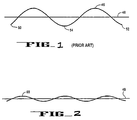
- Fig. 1 illustrates a typical undoped silicate glass (USG) deposition thickness variation plot 46 for a conventional deposition chamber such as the chamber described above.
- the average thickness is shown by base line 48.
- plot 46 there is a relatively steep increase in thickness at end points 50 and 52 of plot 46 corresponding to the periphery 42 of substrate 20.
- the center 54 of plot 46 also dips down substantially as well.
- intermetal dielectric layers With the advent of multilevel metal technology in which three, four, or more layers of metal are formed on the semiconductors, another goal of semiconductor manufacturers is lowering the dielectric constant of insulating layers such as intermetal dielectric layers. Low dielectric constant films are particularly desirable for intermetal dielectric (IMD) layers to reduce the RC time delay of the interconnect metallization, to prevent cross-talk between the different levels of metallization, and to reduce device power consumption.
- IMD intermetal dielectric
- fluorine or other halogen elements such as chlorine or bromine
- fluorine the preferred halogen dopant for silicon oxide films
- fluorine is an electronegative atom that decreases the polarizability of the overall SiOF network.
- Fluorine-doped silicon oxide films are also referred to as fluoro silicate glass (FSG) films.
- the present invention is directed toward an improved deposition chamber that incorporates an improved gas delivery system.
- the gas delivery system helps ensure that the proper ratio of process gases is uniformly delivered across a wafers surface.
- the present invention is also directed toward a method of depositing FSG films having a low dielectric constant and improved uniformity. This is achieved by a combination of (1) the uniform application of the gases (preferably silane, fluorine-supplying gases such as SiF 4 or CF 4 , and oxygen-supplying gases such as O 2 or N 2 O) to the substrate and (2) the selection of optimal flow rates for the gases, which preferably have been determined as a result of tests using the particular chamber.
- the deposited FSG film has a dielectric constant as low as 3.4 or 3.3.
- the dielectric constant of the FSG film is at least below 3.5.
- the improved deposition chamber includes a housing defining a deposition chamber.
- a substrate support is housed within the deposition chamber.
- a first gas distributor has orifices or other exits opening into the deposition chamber in a circumferential pattern spaced apart from and generally overlying the circumferential periphery of the substrate support surface.
- a second gas distributor preferably a center nozzle, is used and is positioned spaced apart from and above the substrate support surface, and a third gas distributor delivers an oxygen-supply gas (e.g., O 2 ) to the chamber through the top of the housing in a region generally centrally above the substrate. This is preferably achieved by passing the oxygen through an annular orifice created between the center nozzle carrying the silane (and any other gases) and a hole in the top of the housing.
- the first gas distributor includes first and second sets of nozzles.
- an FSG film is deposited from a process gas that includes silane, oxygen and SiF 4 .
- Oxygen and SiF 4 are delivered together to the chamber through the first set of nozzles, and silane (or silane and SiF 4 ) is delivered through the second set of nozzles. Mixing the SiF 4 with oxygen and introducing this combination through the first set of nozzles reduces equipment complexity so cost can be reduced.
- Silane (or silane and SiF 4 ) is also injected into the vacuum chamber from the second gas distributor to improve the uniform application of the gases to the substrate over that which is achieved without the use of the second gas distributor, and oxygen is delivered through the third gas distributor.
- oxygen is provided both from the sides through the first set of nozzles of the first gas distributors, preferably mixed with SiF 4 , and also in the same region as silane above the substrate. Also, the passage of the oxygen through the annular orifice keeps reactive gases within the chamber from attacking the seals used between the top of the housing and the body from which the center nozzle extends. This advantage is retained if silane is passed through the annular orifice and oxygen through the center nozzle.
- Film thickness and dielectric constant uniformity is also enhanced by ensuring that the temperature of the substrate remains uniform across the substrate and using a source RF generator designed to achieve sputtering uniformity.
- One of the primary aspects of the method of the present invention is the recognition that it is very important to ensure the uniform distribution of oxygen entering the chamber. This is achieved by flowing oxygen both from the top of the chamber and from the sides of the chamber. Additionally, by the appropriate configuration of the oxygen flow path through the top of the chamber, the oxygen can serve to protect the sealing element from deleterious effects of coming in contact with reactive gases such as fluorine.
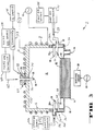
- Fig. 3 illustrates a deposition chamber 2 comprising a housing 4, the housing including a generally cylindrized dielectric enclosure 6 surrounded by two sets of RF inductive coils 8, 9. Enclosure 6 could be made of RF transparent materials other than a dielectric material. Coils 8, 9 are powered by a pair of source RF generators 10, 11. Chamber 2 also includes a water-cooled substrate support 14 having a substrate support surface 16 within the vacuum chamber 18 defined within housing 4. Surface 16 is used to support a substrate 20 within chamber 18. Substrate support 14 acts as a cathode and is connected to a bias RF generator 22 through a matching circuit 24. A generally cylindrical sidewall 30 of housing 4 connects the bottom 32 of housing 4 to dielectric enclosure 6. Sidewall 30 acts as the anode.
- Process gases are introduced to vacuum chamber 18 in the region surrounding substrate 20 through two sets of twelve equally spaced nozzles 34, 34a.
- Nozzles 34, 34a are arranged in a ring-like pattern and are fluidly coupled to gas manifolds 36, 36a, respectively.
- Manifolds 36, 36a are fed process gases from first and second gas sources 35, 35a through first and second gas controllers 37, 37a and first and second gas feed lines 39, 39a.
- Each nozzle 34, 34a has an orifice 38 at its distal end.
- the orifices 38 of nozzles 34, 34a are arranged above the periphery 40 of substrate support 14 and thus above the periphery 42 of substrate 20.
- Vacuum chamber 18 is exhausted through an exhaust port 44.
- the various components of chamber 2 are controlled by a processor (not shown).
- the processor operates under control of a computer program stored in a computer-readable medium (also not shown).
- the computer program dictates the various operating parameters, such as timing, mixture of gases, chamber pressure, substrate support temperature and RF power levels.
- gas delivery component 65 includes a gas pathway 70 formed in a body 72 mounted to the top 75 of enclosure 6.
- a center nozzle 56 passes through an opening 74 formed in top 75.
- Nozzle 56 and opening 74 provide an annular orifice 76 in fluid communication with vacuum chamber 18 and gas pathway 70.
- a fluid seal 78 is provided between body 72 and top 75. Gas thus proceeds through pathway 70, into a region defined between body 72 and top 75 and bounded by fluid seal 78, and finally along annular orifice 76.
- the apparatus of the present invention is used to deposit FSG films from silane, oxygen and SiF 4 precursor gases.
- the present invention preferably supplies a combination of SiF 4 and oxygen from first gas source 35 for introduction into chamber 18 through orifices 38 of nozzles 34. Doing so simplifies the delivery of these gases and helps reduce cost.
- Silane (SiH 4 ) is preferably delivered into chamber 18 from second gas source 35a, through second gas controller 37a, and through nozzles 34a.
- third gas source 58 is preferably used to introduce silane (or, for example, a mixture of silane and SiF 4 ) into chamber 18 from above substrate 20.
- oxygen is also directed into chamber 18 from a position above substrate 20, but along a flow path separate from the flow path of the silane through pathway 70 and annular orifice 76.
- Oxygen can be mixed with a relatively stable gas such as SiF 4 ; however, due to the reactive nature of silane and oxygen, these components must be kept separate until their introduction into chamber 18.
- separate nozzles 34, 34a are used in the region around substrate support 14; also oxygen is introduced through gas pathway 70 formed in a body 72. Pathway 70 is coupled to an oxygen source 71 through an oxygen controller 73. Third gas line 62 passes through body 72 and terminates at center nozzle 56.
- gases such as fluorine compounds, which could otherwise have a deleterious effect on fluid seal 78, are prevented from reaching the fluid seal by the washing effect or scouring effect of the flowing oxygen.
- gases other than oxygen which do not cause seal 78 to deteriorate can also be used.
- oxygen has a relatively long residence time as compared to silane or some other gases. Because of the short residence time of silane, when silane is introduced through orifice 76 it may dissociate relatively quickly leading to particle formation within the orifice and upstream of the orifice in pathways 70. Molecular oxygen has a longer residence time than silane, Thus, this is not a problem when oxygen is delivered through orifice 76 instead.
- Depositing FSG films in this manner results in stable films (substantially no HF or H 2 O outgassing at temperatures up to 450 ⁇ C) having dielectric constants of less than 3.5 and even less than 3.4 or 3.3. These low dielectric constant values are achieved in a generally uniform manner over substrate 20.
- the uniform reduction of the dielectric constant is important because as device sizes are reduced, capacitance between closely spaced conductors will naturally increase. To reduce the capacitance, and thus speed up operation of the devices, the dielectric constant of the deposited dielectric film must be reduced.
- uniform dielectric constants are also dependent upon temperature uniformity across substrate 20 and sputtering uniformity.
- U.S. Patent Application No. 08/641,147 filed April 25, 1996, which is a description of a structure which can be used to achieve more uniform temperature distributions along substrate.
- Varying the total flow of SiF 4 and silane affects deposition rate and thus throughput.
- High throughput requires high bias power from bias power source 22 to create high sputtering and high etching rates.
- High bias power, and thus high throughput, is possible only if temperature uniformity across substrate 20 is achieved since speed of etching is strongly affected by the temperature of the substrate.
- SiF 4 , silane (SiH 4 ) and oxygen to be used creates an entire new layer of complexity. Assuming the total flow rate of silicon (e.g., from SiH 4 and SiF 4 ) remains constant, it is believed that several basic statements can be made regarding the use of these various components. If too little oxygen is used, the deposition rate drops dramatically thus making the process much too inefficient. Too little oxygen can leave the film silicon rich with excess free fluorine incorporated into the film. If too much oxygen is used, the resulting film becomes more USG and the dielectric constant becomes high.
- the optimal amounts of oxygen, SiF 4 and silane at the substrate surface are the stoichiometric proportions.
- flowing stoichiometric proportions of the gases into deposition chambers, including chamber 2 and other deposition chambers would result in gas proportions at the substrate surface which are not the stoichiometric proportions.
- the actual proportions of the gas flowing into the deposition chamber needed to achieve stoichiometric proportions at the substrate surface will vary from the stoichiometric proportions at least in part according to the structure of the specific chamber. The more efficient the chamber, the less gas is wasted so that gas flow rates closer to the stoichiometric amounts can be used.
- the proportions of the three components could be varied in any desired manner to create a number of dielectric films on substrates 20; the dielectric constant at different positions along each dielectric film could then be measured.
- the percentage of SiF 4 should be between about 40% to 60% of the total silicon-supplying gas to reduce or eliminate the problems resulting from too much or too little SiF 4 and silane.
- Oxygen should be between about 60% to 100% of the total silicon-supplying gas.
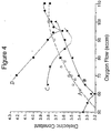
- Fig. 4 illustrates the results of a set of tests conducted varying the ratios of SiF 4 to silane to oxygen. It was found that by selecting a total reactive gas flow rate, that is a flow rate for the combination of SiF 4 and silane (which results in a constant amount of silicon), dividing that total between SiF 4 and silane to arrive at various proportions of SiF 4 and silane, and then, using those proportions, varying the oxygen flow, the graph shown in Fig. 4 of dielectric constant to oxygen flow was created. This type of graph provides very useful data.
- Plot A resulting from 44 sccm SiF 4 to 36.4 sccm silane, results in a dielectric constant which varies from 3.4 at an oxygen flow of about 62 sccm to about 3.8 at an oxygen flow rate of about 110 sccm. It is not clear from this graph where the minimum dielectric constant would be for this ratio of SiF 4 to silane. It appears, however, that the minimum would occur at an unacceptably low oxygen flow rate.
- Plot B having an sccm flow rate ratio of SiF 4 to silane of 36 to 44.4 provides the lowest dielectric constant: about 3.2 at an oxygen flow of 60 sccm.
- Plots C and D have minimum dielectric constants of about 3.5 and 3.6 respectively.
- the present invention provides a useful and efficient way of determining how to achieve films with low dielectric constants using SiF 4 (or another fluorine-supplying gas) and silane chemistry to achieve the reduced dielectric constants. While the above-described method of choosing a single total reactive gas flow rate for each of the tests is presently preferred, other methods for the orderly gathering of dielectric constant information may also be pursued. For example, it may be desired to allow all three variables to change within the overall parameters.
- a film having a low dielectric constant can be deposited on substrate 20 by first determining the appropriate flow rates of SiF 4 , silane and oxygen, typically in the manner discussed above by plotting the results of different tests.
- silane is introduced into chamber 18 from second gas source 35a
- a mixture of silane and SiF 4 is introduced into chamber 18 from third gas source 58
- oxygen is introduced into the chamber from oxygen source 71
- a mixture of oxygen and SiF 4 is introduced into chamber 18 from first gas source 35.
- Argon is also introduced from first and third sources 35, 58.
- Deposition uniformity is also aided by insuring that the temperature of substrate 20 is uniformly controlled over its surface and by the use of a variable frequency source RF generators 10, 11 to help achieve uniform sputtering.
- the above-described embodiment has been designed for substrates 20 having diameters of 8 inches (20 cm). Larger diameter substrates, such as substrates having diameters of 12 inches (30 cm), may call for the use of multiple center nozzles 56a as illustrated in Fig. 5 by the nozzle assembly 56'.
- the deposition thickness variation plot would likely have a three-bump (as in Fig. 3), a four-bump or a five-bump shape.
- the particular shape for the deposition thickness plot would be influenced by the type, number, orientation and spacing of center nozzles 56A and orifices 64.
- oxygen may also be directed into chamber 18 through a number of downwardly and outwardly extending passageways 80 as shown in Fig. 6.
- Each passageway 80 has an orifice 82 where oxygen enters into chamber 18.
- other gases such as argon, may be mixed with one or both of the silane passing through orifice 64 or oxygen passing through annular orifice 76 or orifices 82.
- center nozzle 56 could be replaced by a shower head type of gas distributor having multiple exits or a circular array of gas exits.
- nozzles 34, 34a or 56a could be replaced by, for example, a ring or ring-like structure having gas exits or orifices through which the process gases are delivered into chamber 18. While separate nozzles 34, 34a are preferred, a single set of nozzles 34 could be used to supply silane and SiF 4 but not oxygen.
- Orifice 76 can include a plurality of small apertures arranged in a circular fashion around center nozzle 56 rather than an annular ring.
- oxygen source 71 and third gas source 58 could be switched so that source 71 becomes connected to nozzle 56 and source 58 becomes connected to pathway 70.
- gases besides silane, oxygen and SiF 4 can be employed.
- Other silicon sources such as tetraethyloxysilane (TEOS), other oxygen sources, such as N 2 O, and other fluorine sources such as C 2 F 6 , CF 4 or the like, may be used.
- the chamber of the present invention can be used to deposit other halogen-doped films, USG films, low k carbon films and others.
- oxygen may not be included in the process gas.
- other gases e.g., nitrogen, may be introduced through orifice 76 in these embodiments.
Landscapes
- Chemical & Material Sciences (AREA)
- Engineering & Computer Science (AREA)
- Metallurgy (AREA)
- Chemical Kinetics & Catalysis (AREA)
- Materials Engineering (AREA)
- Mechanical Engineering (AREA)
- General Chemical & Material Sciences (AREA)
- Organic Chemistry (AREA)
- Inorganic Chemistry (AREA)
- Physics & Mathematics (AREA)
- Plasma & Fusion (AREA)
- Analytical Chemistry (AREA)
- Chemical Vapour Deposition (AREA)
- Formation Of Insulating Films (AREA)
- Physical Vapour Deposition (AREA)
Applications Claiming Priority (2)
| Application Number | Priority Date | Filing Date | Title |
|---|---|---|---|
| US851856 | 1986-04-14 | ||
| US08/851,856 US6070551A (en) | 1996-05-13 | 1997-05-06 | Deposition chamber and method for depositing low dielectric constant films |
Publications (1)
| Publication Number | Publication Date |
|---|---|
| EP0877410A1 true EP0877410A1 (de) | 1998-11-11 |
Family
ID=25311887
Family Applications (1)
| Application Number | Title | Priority Date | Filing Date |
|---|---|---|---|
| EP98107646A Withdrawn EP0877410A1 (de) | 1997-05-06 | 1998-04-27 | Verfahren zur Abscheidung von Schichten mit niedriger Dielektrizitätskonstante und Prozessklammer mit Gaszuführungssystem zur Durchführung des Verfahrens |
Country Status (5)
| Country | Link |
|---|---|
| US (5) | US6070551A (de) |
| EP (1) | EP0877410A1 (de) |
| JP (1) | JPH10321613A (de) |
| KR (1) | KR19980086762A (de) |
| TW (1) | TW380279B (de) |
Cited By (8)
| Publication number | Priority date | Publication date | Assignee | Title |
|---|---|---|---|---|
| WO2000030158A1 (en) * | 1998-11-12 | 2000-05-25 | Applied Materials, Inc. | Gas distribution system for a cvd processing chamber |
| EP1073108A1 (de) * | 1999-07-27 | 2001-01-31 | Applied Materials, Inc. | Chemisches Gasphasenabscheidungsverfahren zur Herstellung von dielektrischem Material |
| GB2358085A (en) * | 1999-07-01 | 2001-07-11 | Hyundai Electronics Ind | Method of forming a capacitor with crystalline tantalum oxide nitride TaON dielectric layer by LPCVD |
| US6432259B1 (en) | 1999-12-14 | 2002-08-13 | Applied Materials, Inc. | Plasma reactor cooled ceiling with an array of thermally isolated plasma heated mini-gas distribution plates |
| US6486081B1 (en) | 1998-11-13 | 2002-11-26 | Applied Materials, Inc. | Gas distribution system for a CVD processing chamber |
| KR100688479B1 (ko) * | 2000-08-21 | 2007-03-08 | 삼성전자주식회사 | 균일한 클리닝 가스 공급을 위한 플라즈마 화학 기상 증착챔버 |
| US7651584B2 (en) | 2004-01-16 | 2010-01-26 | Tokyo Electron Limited | Processing apparatus |
| WO2013117576A1 (de) * | 2012-02-09 | 2013-08-15 | Singulus Technologies Ag | Verfahren und vorrichtung zur passivierung von solarzellen mit einer aluminiumoxid-schicht |
Families Citing this family (161)
| Publication number | Priority date | Publication date | Assignee | Title |
|---|---|---|---|---|
| US5772771A (en) * | 1995-12-13 | 1998-06-30 | Applied Materials, Inc. | Deposition chamber for improved deposition thickness uniformity |
| US6070551A (en) * | 1996-05-13 | 2000-06-06 | Applied Materials, Inc. | Deposition chamber and method for depositing low dielectric constant films |
| US6184158B1 (en) * | 1996-12-23 | 2001-02-06 | Lam Research Corporation | Inductively coupled plasma CVD |
| US6112696A (en) * | 1998-02-17 | 2000-09-05 | Dry Plasma Systems, Inc. | Downstream plasma using oxygen gas mixture |
| KR100292410B1 (ko) * | 1998-09-23 | 2001-06-01 | 윤종용 | 불순물 오염이 억제된 반도체 제조용 반응 챔버 |
| US6230651B1 (en) * | 1998-12-30 | 2001-05-15 | Lam Research Corporation | Gas injection system for plasma processing |
| KR100331544B1 (ko) * | 1999-01-18 | 2002-04-06 | 윤종용 | 반응챔버에 가스를 유입하는 방법 및 이에 사용되는 샤워헤드 |
| JP4066292B2 (ja) * | 1999-06-09 | 2008-03-26 | 株式会社小糸製作所 | 自動車用プラスチック部品の保護膜形成方法 |
| US6165915A (en) * | 1999-08-11 | 2000-12-26 | Taiwan Semiconductor Manufacturing Company | Forming halogen doped glass dielectric layer with enhanced stability |
| DE60038811D1 (de) * | 1999-11-15 | 2008-06-19 | Lam Res Corp | Behandlungsvorrichtungen |
| US6514378B1 (en) * | 2000-03-31 | 2003-02-04 | Lam Research Corporation | Method for improving uniformity and reducing etch rate variation of etching polysilicon |
| JP2001308086A (ja) * | 2000-04-18 | 2001-11-02 | Nec Corp | 膜形成方法 |
| US6468927B1 (en) * | 2000-05-19 | 2002-10-22 | Applied Materials, Inc. | Method of depositing a nitrogen-doped FSG layer |
| KR100406173B1 (ko) * | 2000-06-13 | 2003-11-19 | 주식회사 하이닉스반도체 | 촉매 분사 수단을 구비한 히터 블록 |
| TW521386B (en) * | 2000-06-28 | 2003-02-21 | Mitsubishi Heavy Ind Ltd | Hexagonal boron nitride film with low dielectric constant, layer dielectric film and method of production thereof, and plasma CVD apparatus |
| KR100436941B1 (ko) * | 2000-11-07 | 2004-06-23 | 주성엔지니어링(주) | 박막 증착 장치 및 그 방법 |
| US6689220B1 (en) * | 2000-11-22 | 2004-02-10 | Simplus Systems Corporation | Plasma enhanced pulsed layer deposition |
| US6660662B2 (en) * | 2001-01-26 | 2003-12-09 | Applied Materials, Inc. | Method of reducing plasma charge damage for plasma processes |
| US6596653B2 (en) * | 2001-05-11 | 2003-07-22 | Applied Materials, Inc. | Hydrogen assisted undoped silicon oxide deposition process for HDP-CVD |
| US6740601B2 (en) * | 2001-05-11 | 2004-05-25 | Applied Materials Inc. | HDP-CVD deposition process for filling high aspect ratio gaps |
| US20030012875A1 (en) * | 2001-07-10 | 2003-01-16 | Shreyas Kher | CVD BST film composition and property control with thickness below 200 A for DRAM capacitor application with size at 0.1mum or below |
| US6797605B2 (en) * | 2001-07-26 | 2004-09-28 | Chartered Semiconductor Manufacturing Ltd. | Method to improve adhesion of dielectric films in damascene interconnects |
| KR100434516B1 (ko) * | 2001-08-27 | 2004-06-05 | 주성엔지니어링(주) | 반도체 제조장치 |
| US20030070620A1 (en) | 2001-10-15 | 2003-04-17 | Cooperberg David J. | Tunable multi-zone gas injection system |
| KR20030037092A (ko) * | 2001-11-02 | 2003-05-12 | 주성엔지니어링(주) | 반도체 제조장치 |
| US6730367B2 (en) * | 2002-03-05 | 2004-05-04 | Micron Technology, Inc. | Atomic layer deposition method with point of use generated reactive gas species |
| EP2050839A3 (de) * | 2002-03-08 | 2009-05-13 | Canon Anelva Corporation | Verfahren und Vorrichtung zum Herstellen von Metall-Schichten |
| US6812153B2 (en) * | 2002-04-30 | 2004-11-02 | Applied Materials Inc. | Method for high aspect ratio HDP CVD gapfill |
| US6838114B2 (en) | 2002-05-24 | 2005-01-04 | Micron Technology, Inc. | Methods for controlling gas pulsing in processes for depositing materials onto micro-device workpieces |
| US6821347B2 (en) | 2002-07-08 | 2004-11-23 | Micron Technology, Inc. | Apparatus and method for depositing materials onto microelectronic workpieces |
| US6955725B2 (en) | 2002-08-15 | 2005-10-18 | Micron Technology, Inc. | Reactors with isolated gas connectors and methods for depositing materials onto micro-device workpieces |
| US6884296B2 (en) * | 2002-08-23 | 2005-04-26 | Micron Technology, Inc. | Reactors having gas distributors and methods for depositing materials onto micro-device workpieces |
| US6808748B2 (en) * | 2003-01-23 | 2004-10-26 | Applied Materials, Inc. | Hydrogen assisted HDP-CVD deposition process for aggressive gap-fill technology |
| WO2004088729A1 (en) * | 2003-03-26 | 2004-10-14 | Tokyo Electron Limited | Chemical processing system and method |
| US7335396B2 (en) | 2003-04-24 | 2008-02-26 | Micron Technology, Inc. | Methods for controlling mass flow rates and pressures in passageways coupled to reaction chambers and systems for depositing material onto microfeature workpieces in reaction chambers |
| DE10320597A1 (de) * | 2003-04-30 | 2004-12-02 | Aixtron Ag | Verfahren und Vorrichtung zum Abscheiden von Halbleiterschichten mit zwei Prozessgasen, von denen das eine vorkonditioniert ist |
| US6958112B2 (en) * | 2003-05-27 | 2005-10-25 | Applied Materials, Inc. | Methods and systems for high-aspect-ratio gapfill using atomic-oxygen generation |
| US7344755B2 (en) | 2003-08-21 | 2008-03-18 | Micron Technology, Inc. | Methods and apparatus for processing microfeature workpieces; methods for conditioning ALD reaction chambers |
| US7235138B2 (en) | 2003-08-21 | 2007-06-26 | Micron Technology, Inc. | Microfeature workpiece processing apparatus and methods for batch deposition of materials on microfeature workpieces |
| US7422635B2 (en) | 2003-08-28 | 2008-09-09 | Micron Technology, Inc. | Methods and apparatus for processing microfeature workpieces, e.g., for depositing materials on microfeature workpieces |
| US6903031B2 (en) * | 2003-09-03 | 2005-06-07 | Applied Materials, Inc. | In-situ-etch-assisted HDP deposition using SiF4 and hydrogen |
| US7056806B2 (en) | 2003-09-17 | 2006-06-06 | Micron Technology, Inc. | Microfeature workpiece processing apparatus and methods for controlling deposition of materials on microfeature workpieces |
| US7282239B2 (en) | 2003-09-18 | 2007-10-16 | Micron Technology, Inc. | Systems and methods for depositing material onto microfeature workpieces in reaction chambers |
| US7323231B2 (en) | 2003-10-09 | 2008-01-29 | Micron Technology, Inc. | Apparatus and methods for plasma vapor deposition processes |
| US7581511B2 (en) | 2003-10-10 | 2009-09-01 | Micron Technology, Inc. | Apparatus and methods for manufacturing microfeatures on workpieces using plasma vapor processes |
| US7647886B2 (en) | 2003-10-15 | 2010-01-19 | Micron Technology, Inc. | Systems for depositing material onto workpieces in reaction chambers and methods for removing byproducts from reaction chambers |
| JP4306403B2 (ja) | 2003-10-23 | 2009-08-05 | 東京エレクトロン株式会社 | シャワーヘッド構造及びこれを用いた成膜装置 |
| US7258892B2 (en) | 2003-12-10 | 2007-08-21 | Micron Technology, Inc. | Methods and systems for controlling temperature during microfeature workpiece processing, e.g., CVD deposition |
| US7906393B2 (en) * | 2004-01-28 | 2011-03-15 | Micron Technology, Inc. | Methods for forming small-scale capacitor structures |
| US20060048707A1 (en) * | 2004-09-03 | 2006-03-09 | Applied Materials, Inc. | Anti-clogging nozzle for semiconductor processing |
| US7584942B2 (en) * | 2004-03-31 | 2009-09-08 | Micron Technology, Inc. | Ampoules for producing a reaction gas and systems for depositing materials onto microfeature workpieces in reaction chambers |
| US8133554B2 (en) | 2004-05-06 | 2012-03-13 | Micron Technology, Inc. | Methods for depositing material onto microfeature workpieces in reaction chambers and systems for depositing materials onto microfeature workpieces |
| US20050260356A1 (en) * | 2004-05-18 | 2005-11-24 | Applied Materials, Inc. | Microcontamination abatement in semiconductor processing |
| US7699932B2 (en) | 2004-06-02 | 2010-04-20 | Micron Technology, Inc. | Reactors, systems and methods for depositing thin films onto microfeature workpieces |
| US7229931B2 (en) * | 2004-06-16 | 2007-06-12 | Applied Materials, Inc. | Oxygen plasma treatment for enhanced HDP-CVD gapfill |
| KR101033123B1 (ko) * | 2004-06-30 | 2011-05-11 | 엘지디스플레이 주식회사 | 액정표시장치의 제조를 위한 챔버형 장치 |
| US7183227B1 (en) | 2004-07-01 | 2007-02-27 | Applied Materials, Inc. | Use of enhanced turbomolecular pump for gapfill deposition using high flows of low-mass fluent gas |
| US20060042754A1 (en) * | 2004-07-30 | 2006-03-02 | Tokyo Electron Limited | Plasma etching apparatus |
| KR101309334B1 (ko) * | 2004-08-02 | 2013-09-16 | 비코 인스트루먼츠 인코포레이티드 | 화학적 기상 증착 반응기용 멀티 가스 분배 인젝터 |
| US7250373B2 (en) * | 2004-08-27 | 2007-07-31 | Applied Materials, Inc. | Method and apparatus for etching material layers with high uniformity of a lateral etch rate across a substrate |
| US7087536B2 (en) * | 2004-09-01 | 2006-08-08 | Applied Materials | Silicon oxide gapfill deposition using liquid precursors |
| KR100589046B1 (ko) * | 2004-09-23 | 2006-06-12 | 삼성전자주식회사 | 박막 형성 방법 |
| US7465475B2 (en) * | 2004-11-09 | 2008-12-16 | Eastman Kodak Company | Method for controlling the deposition of vaporized organic material |
| US7510624B2 (en) * | 2004-12-17 | 2009-03-31 | Applied Materials, Inc. | Self-cooling gas delivery apparatus under high vacuum for high density plasma applications |
| US20060196417A1 (en) * | 2005-03-03 | 2006-09-07 | Taiwan Semiconductor Manufacturing Co., Ltd. | Gas distribution systems for deposition processes |
| US7722719B2 (en) * | 2005-03-07 | 2010-05-25 | Applied Materials, Inc. | Gas baffle and distributor for semiconductor processing chamber |
| US7972441B2 (en) * | 2005-04-05 | 2011-07-05 | Applied Materials, Inc. | Thermal oxidation of silicon using ozone |
| KR100897176B1 (ko) * | 2005-07-20 | 2009-05-14 | 삼성모바일디스플레이주식회사 | 유도 결합형 플라즈마 처리 장치 |
| US7651587B2 (en) * | 2005-08-11 | 2010-01-26 | Applied Materials, Inc. | Two-piece dome with separate RF coils for inductively coupled plasma reactors |
| US8097120B2 (en) * | 2006-02-21 | 2012-01-17 | Lam Research Corporation | Process tuning gas injection from the substrate edge |
| US20070227659A1 (en) * | 2006-03-31 | 2007-10-04 | Tokyo Electron Limited | Plasma etching apparatus |
| US7902080B2 (en) | 2006-05-30 | 2011-03-08 | Applied Materials, Inc. | Deposition-plasma cure cycle process to enhance film quality of silicon dioxide |
| US7825038B2 (en) | 2006-05-30 | 2010-11-02 | Applied Materials, Inc. | Chemical vapor deposition of high quality flow-like silicon dioxide using a silicon containing precursor and atomic oxygen |
| US7498273B2 (en) | 2006-05-30 | 2009-03-03 | Applied Materials, Inc. | Formation of high quality dielectric films of silicon dioxide for STI: usage of different siloxane-based precursors for harp II—remote plasma enhanced deposition processes |
| US7790634B2 (en) | 2006-05-30 | 2010-09-07 | Applied Materials, Inc | Method for depositing and curing low-k films for gapfill and conformal film applications |
| US8232176B2 (en) | 2006-06-22 | 2012-07-31 | Applied Materials, Inc. | Dielectric deposition and etch back processes for bottom up gapfill |
| KR101352365B1 (ko) * | 2006-08-09 | 2014-01-16 | 엘아이지에이디피 주식회사 | 플라즈마 처리장치 |
| US20080124944A1 (en) * | 2006-11-28 | 2008-05-29 | Applied Materials, Inc. | Gas baffle and distributor for semiconductor processing chamber |
| US20080121177A1 (en) * | 2006-11-28 | 2008-05-29 | Applied Materials, Inc. | Dual top gas feed through distributor for high density plasma chamber |
| US7740706B2 (en) * | 2006-11-28 | 2010-06-22 | Applied Materials, Inc. | Gas baffle and distributor for semiconductor processing chamber |
| US7758698B2 (en) * | 2006-11-28 | 2010-07-20 | Applied Materials, Inc. | Dual top gas feed through distributor for high density plasma chamber |
| WO2008144658A1 (en) * | 2007-05-17 | 2008-11-27 | Exatec, Llc | Apparatus and method for depositing multiple coating materials in a common plasma coating zone |
| US7745352B2 (en) | 2007-08-27 | 2010-06-29 | Applied Materials, Inc. | Curing methods for silicon dioxide thin films deposited from alkoxysilane precursor with harp II process |
| US7803722B2 (en) | 2007-10-22 | 2010-09-28 | Applied Materials, Inc | Methods for forming a dielectric layer within trenches |
| US7541297B2 (en) | 2007-10-22 | 2009-06-02 | Applied Materials, Inc. | Method and system for improving dielectric film quality for void free gap fill |
| US7867923B2 (en) | 2007-10-22 | 2011-01-11 | Applied Materials, Inc. | High quality silicon oxide films by remote plasma CVD from disilane precursors |
| US7943531B2 (en) | 2007-10-22 | 2011-05-17 | Applied Materials, Inc. | Methods for forming a silicon oxide layer over a substrate |
| US7939447B2 (en) * | 2007-10-26 | 2011-05-10 | Asm America, Inc. | Inhibitors for selective deposition of silicon containing films |
| US7964040B2 (en) | 2007-11-08 | 2011-06-21 | Applied Materials, Inc. | Multi-port pumping system for substrate processing chambers |
| US8137463B2 (en) * | 2007-12-19 | 2012-03-20 | Applied Materials, Inc. | Dual zone gas injection nozzle |
| US7655543B2 (en) * | 2007-12-21 | 2010-02-02 | Asm America, Inc. | Separate injection of reactive species in selective formation of films |
| US7678715B2 (en) * | 2007-12-21 | 2010-03-16 | Applied Materials, Inc. | Low wet etch rate silicon nitride film |
| KR101003382B1 (ko) * | 2008-02-13 | 2010-12-22 | 주식회사 유진테크 | 플라즈마 처리장치 및 방법 |
| CN101772833B (zh) * | 2008-02-20 | 2012-04-18 | 东京毅力科创株式会社 | 气体供给装置 |
| US8153348B2 (en) | 2008-02-20 | 2012-04-10 | Applied Materials, Inc. | Process sequence for formation of patterned hard mask film (RFP) without need for photoresist or dry etch |
| US20090221149A1 (en) * | 2008-02-28 | 2009-09-03 | Hammond Iv Edward P | Multiple port gas injection system utilized in a semiconductor processing system |
| US8357435B2 (en) | 2008-05-09 | 2013-01-22 | Applied Materials, Inc. | Flowable dielectric equipment and processes |
| WO2010041213A1 (en) * | 2008-10-08 | 2010-04-15 | Abcd Technology Sarl | Vapor phase deposition system |
| JP2012506620A (ja) * | 2008-10-21 | 2012-03-15 | アプライド マテリアルズ インコーポレイテッド | チャンバをクリーニングするプラズマ発生源とプロセス |
| US8486191B2 (en) | 2009-04-07 | 2013-07-16 | Asm America, Inc. | Substrate reactor with adjustable injectors for mixing gases within reaction chamber |
| US8980382B2 (en) | 2009-12-02 | 2015-03-17 | Applied Materials, Inc. | Oxygen-doping for non-carbon radical-component CVD films |
| US7935643B2 (en) | 2009-08-06 | 2011-05-03 | Applied Materials, Inc. | Stress management for tensile films |
| US8741788B2 (en) | 2009-08-06 | 2014-06-03 | Applied Materials, Inc. | Formation of silicon oxide using non-carbon flowable CVD processes |
| US7989365B2 (en) | 2009-08-18 | 2011-08-02 | Applied Materials, Inc. | Remote plasma source seasoning |
| US8449942B2 (en) | 2009-11-12 | 2013-05-28 | Applied Materials, Inc. | Methods of curing non-carbon flowable CVD films |
| SG181670A1 (en) | 2009-12-30 | 2012-07-30 | Applied Materials Inc | Dielectric film growth with radicals produced using flexible nitrogen/hydrogen ratio |
| US8329262B2 (en) | 2010-01-05 | 2012-12-11 | Applied Materials, Inc. | Dielectric film formation using inert gas excitation |
| JP2013517616A (ja) | 2010-01-06 | 2013-05-16 | アプライド マテリアルズ インコーポレイテッド | 酸化物ライナを使用する流動可能な誘電体 |
| WO2011084752A2 (en) | 2010-01-07 | 2011-07-14 | Applied Materials, Inc. | In-situ ozone cure for radical-component cvd |
| KR101092122B1 (ko) * | 2010-02-23 | 2011-12-12 | 주식회사 디엠에스 | 에칭 프로파일 제어를 위한 가스 인젝션 시스템 |
| WO2011109148A2 (en) | 2010-03-05 | 2011-09-09 | Applied Materials, Inc. | Conformal layers by radical-component cvd |
| US8236708B2 (en) | 2010-03-09 | 2012-08-07 | Applied Materials, Inc. | Reduced pattern loading using bis(diethylamino)silane (C8H22N2Si) as silicon precursor |
| US7994019B1 (en) | 2010-04-01 | 2011-08-09 | Applied Materials, Inc. | Silicon-ozone CVD with reduced pattern loading using incubation period deposition |
| US8476142B2 (en) | 2010-04-12 | 2013-07-02 | Applied Materials, Inc. | Preferential dielectric gapfill |
| US8524004B2 (en) | 2010-06-16 | 2013-09-03 | Applied Materials, Inc. | Loadlock batch ozone cure |
| US8318584B2 (en) | 2010-07-30 | 2012-11-27 | Applied Materials, Inc. | Oxide-rich liner layer for flowable CVD gapfill |
| US9285168B2 (en) | 2010-10-05 | 2016-03-15 | Applied Materials, Inc. | Module for ozone cure and post-cure moisture treatment |
| US8664127B2 (en) | 2010-10-15 | 2014-03-04 | Applied Materials, Inc. | Two silicon-containing precursors for gapfill enhancing dielectric liner |
| US10658161B2 (en) * | 2010-10-15 | 2020-05-19 | Applied Materials, Inc. | Method and apparatus for reducing particle defects in plasma etch chambers |
| US10283321B2 (en) | 2011-01-18 | 2019-05-07 | Applied Materials, Inc. | Semiconductor processing system and methods using capacitively coupled plasma |
| US20120180954A1 (en) | 2011-01-18 | 2012-07-19 | Applied Materials, Inc. | Semiconductor processing system and methods using capacitively coupled plasma |
| US8450191B2 (en) | 2011-01-24 | 2013-05-28 | Applied Materials, Inc. | Polysilicon films by HDP-CVD |
| US8716154B2 (en) | 2011-03-04 | 2014-05-06 | Applied Materials, Inc. | Reduced pattern loading using silicon oxide multi-layers |
| US8445078B2 (en) | 2011-04-20 | 2013-05-21 | Applied Materials, Inc. | Low temperature silicon oxide conversion |
| US9512520B2 (en) * | 2011-04-25 | 2016-12-06 | Applied Materials, Inc. | Semiconductor substrate processing system |
| US8466073B2 (en) | 2011-06-03 | 2013-06-18 | Applied Materials, Inc. | Capping layer for reduced outgassing |
| JP5902896B2 (ja) * | 2011-07-08 | 2016-04-13 | 東京エレクトロン株式会社 | 基板処理装置 |
| US9404178B2 (en) | 2011-07-15 | 2016-08-02 | Applied Materials, Inc. | Surface treatment and deposition for reduced outgassing |
| US8617989B2 (en) | 2011-09-26 | 2013-12-31 | Applied Materials, Inc. | Liner property improvement |
| US8551891B2 (en) | 2011-10-04 | 2013-10-08 | Applied Materials, Inc. | Remote plasma burn-in |
| TWI638587B (zh) | 2011-10-05 | 2018-10-11 | 美商應用材料股份有限公司 | 對稱電漿處理腔室 |
| US9941100B2 (en) | 2011-12-16 | 2018-04-10 | Taiwan Semiconductor Manufacturing Company, Ltd. | Adjustable nozzle for plasma deposition and a method of controlling the adjustable nozzle |
| US8889566B2 (en) | 2012-09-11 | 2014-11-18 | Applied Materials, Inc. | Low cost flowable dielectric films |
| US9018108B2 (en) | 2013-01-25 | 2015-04-28 | Applied Materials, Inc. | Low shrinkage dielectric films |
| US9790596B1 (en) * | 2013-01-30 | 2017-10-17 | Kyocera Corporation | Gas nozzle and plasma device employing same |
| CN107424901B (zh) | 2013-03-12 | 2019-06-11 | 应用材料公司 | 具有方位角与径向分布控制的多区域气体注入组件 |
| US8993446B2 (en) * | 2013-04-23 | 2015-03-31 | Globalfoundries Inc. | Method of forming a dielectric film |
| KR102264053B1 (ko) * | 2013-05-01 | 2021-06-11 | 어플라이드 머티어리얼스, 인코포레이티드 | Epi 챔버 유동 조작을 위한 주입구 및 배기구 설계 |
| JP6292769B2 (ja) * | 2013-05-30 | 2018-03-14 | 小島プレス工業株式会社 | プラズマcvd装置及びプラズマcvd膜の形成方法 |
| CN106414796B (zh) * | 2014-04-09 | 2022-01-11 | 布勒阿尔策瑙股份有限公司 | 真空室的具有气体引导机构的气体分配装置 |
| US9412581B2 (en) | 2014-07-16 | 2016-08-09 | Applied Materials, Inc. | Low-K dielectric gapfill by flowable deposition |
| US10465288B2 (en) * | 2014-08-15 | 2019-11-05 | Applied Materials, Inc. | Nozzle for uniform plasma processing |
| JP5840268B1 (ja) * | 2014-08-25 | 2016-01-06 | 株式会社日立国際電気 | 基板処理装置、半導体装置の製造方法および記録媒体 |
| US20160225652A1 (en) | 2015-02-03 | 2016-08-04 | Applied Materials, Inc. | Low temperature chuck for plasma processing systems |
| JP6126155B2 (ja) | 2015-03-31 | 2017-05-10 | 株式会社日立国際電気 | 半導体装置の製造方法、プログラムおよび基板処理装置 |
| KR102638572B1 (ko) * | 2015-06-17 | 2024-02-21 | 어플라이드 머티어리얼스, 인코포레이티드 | 프로세스 챔버 내의 가스 제어 |
| JP6153975B2 (ja) * | 2015-08-07 | 2017-06-28 | 株式会社日立国際電気 | 半導体装置の製造方法、基板処理システム、プログラム、記録媒体および基板処理装置 |
| CN108292588B (zh) * | 2015-12-04 | 2022-02-18 | 应用材料公司 | 用以防止hdp-cvd腔室电弧放电的先进涂层方法及材料 |
| CN106876299B (zh) * | 2015-12-11 | 2019-08-23 | 北京北方华创微电子装备有限公司 | 半导体加工设备 |
| TWI582885B (zh) * | 2015-12-30 | 2017-05-11 | 國立中央大學 | 低溫製造組織工程用支架的平台結構及低溫製造組織工程用支架的製造方法 |
| KR102553629B1 (ko) * | 2016-06-17 | 2023-07-11 | 삼성전자주식회사 | 플라즈마 처리 장치 |
| US10896806B2 (en) * | 2016-11-03 | 2021-01-19 | En2Core Technology, Inc. | Inductive coil structure and inductively coupled plasma generation system |
| CN107345294A (zh) * | 2017-07-26 | 2017-11-14 | 北京芯微诺达科技有限公司 | 一种等离子体设备的进气结构 |
| US11326256B2 (en) * | 2018-12-10 | 2022-05-10 | Applied Materials, Inc. | Dome stress isolating layer |
| CN109887872B (zh) * | 2019-03-29 | 2024-11-15 | 华南理工大学 | 用于制备凹槽栅增强型器件的精准刻蚀装置及其刻蚀方法 |
| JP6922959B2 (ja) * | 2019-09-20 | 2021-08-18 | 株式会社明電舎 | 酸化膜形成装置 |
| JP7330079B2 (ja) * | 2019-11-28 | 2023-08-21 | 東京エレクトロン株式会社 | プラズマ処理装置 |
| CN112899637B (zh) * | 2019-12-04 | 2023-03-31 | 江苏菲沃泰纳米科技股份有限公司 | 镀膜装置的进气系统 |
| US12131888B2 (en) * | 2020-08-31 | 2024-10-29 | Tokyo Electron Limited | Gas cluster assisted plasma processing |
| KR102949847B1 (ko) * | 2021-04-29 | 2026-04-07 | 에이에스엠 아이피 홀딩 비.브이. | 반응기 시스템 및 반응기 시스템을 세정하기 위한 방법 |
| CN113862624B (zh) * | 2021-09-27 | 2023-03-21 | 上海集成电路材料研究院有限公司 | 溅射沉积设备及溅射沉积方法 |
Citations (5)
| Publication number | Priority date | Publication date | Assignee | Title |
|---|---|---|---|---|
| US5453124A (en) * | 1992-12-30 | 1995-09-26 | Texas Instruments Incorporated | Programmable multizone gas injector for single-wafer semiconductor processing equipment |
| EP0701283A2 (de) * | 1994-09-12 | 1996-03-13 | Nec Corporation | Halbleiteranordnung mit einer Schicht aus amorphem Kohlenstoff und Verfahren zur Herstellung |
| EP0704885A2 (de) * | 1994-09-30 | 1996-04-03 | International Business Machines Corporation | Verfahren zur Ablagerung einer fluordotierten Schicht |
| US5522934A (en) * | 1994-04-26 | 1996-06-04 | Tokyo Electron Limited | Plasma processing apparatus using vertical gas inlets one on top of another |
| EP0807694A1 (de) * | 1996-05-13 | 1997-11-19 | Applied Materials, Inc. | Aufdampfungskammer und Verfahren zur Herstellung eines Films mit einer niedrigen Dielektrizitätskonstante |
Family Cites Families (54)
| Publication number | Priority date | Publication date | Assignee | Title |
|---|---|---|---|---|
| US3511703A (en) * | 1963-09-20 | 1970-05-12 | Motorola Inc | Method for depositing mixed oxide films containing aluminum oxide |
| US3502502A (en) * | 1967-01-05 | 1970-03-24 | Motorola Inc | Process for depositing a tantalum oxide containing coating |
| US3717439A (en) * | 1970-11-18 | 1973-02-20 | Tokyo Shibaura Electric Co | Vapour phase reaction apparatus |
| JPS6047202B2 (ja) * | 1976-01-13 | 1985-10-21 | 東北大学金属材料研究所長 | 超硬高純度の配向多結晶質窒化珪素 |
| EP0000599B1 (de) | 1977-07-25 | 1983-02-02 | EASTMAN KODAK COMPANY (a New Jersey corporation) | Elektrophotosensible Teilchen für photoelektrophoretische Bilderzeugung |
| JPS54111771A (en) * | 1978-02-22 | 1979-09-01 | Toshiba Corp | Gas phase reaction unit of semiconductor substrate |
| JPS61231716A (ja) * | 1985-04-08 | 1986-10-16 | Hitachi Ltd | 成膜装置 |
| JPS61263118A (ja) * | 1985-05-15 | 1986-11-21 | Sharp Corp | プラズマcvd装置 |
| US4654521A (en) * | 1985-09-16 | 1987-03-31 | Eastman Kodak Company | Self measuring illumination device |
| US4834022A (en) * | 1985-11-08 | 1989-05-30 | Focus Semiconductor Systems, Inc. | CVD reactor and gas injection system |
| JPS62156270A (ja) * | 1985-12-27 | 1987-07-11 | Canon Inc | 堆積膜形成装置 |
| JPS62228478A (ja) * | 1986-03-31 | 1987-10-07 | Canon Inc | 堆積膜形成装置 |
| JPH0830273B2 (ja) * | 1986-07-10 | 1996-03-27 | 株式会社東芝 | 薄膜形成方法及び装置 |
| JPS6376879A (ja) * | 1986-09-18 | 1988-04-07 | Hitachi Electronics Eng Co Ltd | Cvd薄膜形成装置 |
| JPS63260124A (ja) * | 1987-04-17 | 1988-10-27 | Nippon Telegr & Teleph Corp <Ntt> | 気相成長装置 |
| FR2614317B1 (fr) * | 1987-04-22 | 1989-07-13 | Air Liquide | Procede de protection de substrat polymerique par depot par plasma de composes du type oxynitrure de silicium et dispositif pour sa mise en oeuvre. |
| JPS63293165A (ja) * | 1987-05-27 | 1988-11-30 | Hitachi Ltd | 処理装置 |
| DE3885833T2 (de) * | 1987-09-22 | 1994-03-24 | Nippon Electric Co | Chemischer Dampfabscheidungsapparat für die Herstellung von hochqualitativen epitaktischen Schichten mit gleichmässiger Dichte. |
| JPH01171228A (ja) * | 1987-12-25 | 1989-07-06 | Hitachi Ltd | 処理装置 |
| DE3833232A1 (de) * | 1988-09-30 | 1990-04-05 | Leybold Ag | Verfahren und vorrichtung zum verdampfen von bei raumtemperatur fluessigen monomeren |
| JPH02126632A (ja) | 1988-11-05 | 1990-05-15 | Nippon Telegr & Teleph Corp <Ntt> | 化合物半導体結晶層の気相成長方法及びそれに用いる反応管 |
| JPH02222134A (ja) * | 1989-02-23 | 1990-09-04 | Nobuo Mikoshiba | 薄膜形成装置 |
| US5134965A (en) * | 1989-06-16 | 1992-08-04 | Hitachi, Ltd. | Processing apparatus and method for plasma processing |
| FR2653633B1 (fr) * | 1989-10-19 | 1991-12-20 | Commissariat Energie Atomique | Dispositif de traitement chimique assiste par un plasma de diffusion. |
| US5447570A (en) * | 1990-04-23 | 1995-09-05 | Genus, Inc. | Purge gas in wafer coating area selection |
| US5200232A (en) * | 1990-12-11 | 1993-04-06 | Lam Research Corporation | Reaction chamber design and method to minimize particle generation in chemical vapor deposition reactors |
| JP2699695B2 (ja) * | 1991-06-07 | 1998-01-19 | 日本電気株式会社 | 化学気相成長法 |
| JPH0521393A (ja) * | 1991-07-11 | 1993-01-29 | Sony Corp | プラズマ処理装置 |
| JP2580928Y2 (ja) * | 1991-08-22 | 1998-09-17 | 日本電気株式会社 | 気相成長装置 |
| US5387289A (en) * | 1992-09-22 | 1995-02-07 | Genus, Inc. | Film uniformity by selective pressure gradient control |
| US5346578A (en) * | 1992-11-04 | 1994-09-13 | Novellus Systems, Inc. | Induction plasma source |
| KR0131439B1 (ko) * | 1992-11-24 | 1998-04-14 | 나카무라 타메아키 | 반도체장치 및 그 제조방법 |
| JPH086181B2 (ja) * | 1992-11-30 | 1996-01-24 | 日本電気株式会社 | 化学気相成長法および化学気相成長装置 |
| US5427625A (en) * | 1992-12-18 | 1995-06-27 | Tokyo Electron Kabushiki Kaisha | Method for cleaning heat treatment processing apparatus |
| JP2667364B2 (ja) | 1993-08-16 | 1997-10-27 | キヤノン販売株式会社 | 成膜装置 |
| US5614055A (en) | 1993-08-27 | 1997-03-25 | Applied Materials, Inc. | High density plasma CVD and etching reactor |
| JPH07161642A (ja) | 1993-12-03 | 1995-06-23 | Kobe Steel Ltd | プラズマ処理装置 |
| TW296534B (de) * | 1993-12-17 | 1997-01-21 | Tokyo Electron Co Ltd | |
| US5620523A (en) * | 1994-04-11 | 1997-04-15 | Canon Sales Co., Inc. | Apparatus for forming film |
| JP3243125B2 (ja) | 1994-06-27 | 2002-01-07 | 東京エレクトロン株式会社 | 処理装置 |
| GB9410567D0 (en) * | 1994-05-26 | 1994-07-13 | Philips Electronics Uk Ltd | Plasma treatment and apparatus in electronic device manufacture |
| TW283250B (en) * | 1995-07-10 | 1996-08-11 | Watkins Johnson Co | Plasma enhanced chemical processing reactor and method |
| TW279240B (en) * | 1995-08-30 | 1996-06-21 | Applied Materials Inc | Parallel-plate icp source/rf bias electrode head |
| TW356554B (en) * | 1995-10-23 | 1999-04-21 | Watkins Johnson Co | Gas injection system for semiconductor processing |
| US5772771A (en) * | 1995-12-13 | 1998-06-30 | Applied Materials, Inc. | Deposition chamber for improved deposition thickness uniformity |
| US6200412B1 (en) | 1996-02-16 | 2001-03-13 | Novellus Systems, Inc. | Chemical vapor deposition system including dedicated cleaning gas injection |
| US6363264B1 (en) * | 1996-02-23 | 2002-03-26 | Nokia Mobile Phones Limited | Radio telephone |
| US6070551A (en) * | 1996-05-13 | 2000-06-06 | Applied Materials, Inc. | Deposition chamber and method for depositing low dielectric constant films |
| US6170428B1 (en) * | 1996-07-15 | 2001-01-09 | Applied Materials, Inc. | Symmetric tunable inductively coupled HDP-CVD reactor |
| JP3584644B2 (ja) | 1996-12-13 | 2004-11-04 | 富士ゼロックス株式会社 | 画像形成装置 |
| US6228781B1 (en) * | 1997-04-02 | 2001-05-08 | Applied Materials, Inc. | Sequential in-situ heating and deposition of halogen-doped silicon oxide |
| US6083344A (en) * | 1997-05-29 | 2000-07-04 | Applied Materials, Inc. | Multi-zone RF inductively coupled source configuration |
| US5994662A (en) * | 1997-05-29 | 1999-11-30 | Applied Materials, Inc. | Unique baffle to deflect remote plasma clean gases |
| US6143078A (en) * | 1998-11-13 | 2000-11-07 | Applied Materials, Inc. | Gas distribution system for a CVD processing chamber |
-
1997
- 1997-05-06 US US08/851,856 patent/US6070551A/en not_active Expired - Lifetime
-
1998
- 1998-04-27 EP EP98107646A patent/EP0877410A1/de not_active Withdrawn
- 1998-05-01 JP JP10122227A patent/JPH10321613A/ja not_active Withdrawn
- 1998-05-06 TW TW087107033A patent/TW380279B/zh active
- 1998-05-06 KR KR1019980016047A patent/KR19980086762A/ko not_active Withdrawn
-
2000
- 2000-02-29 US US09/515,574 patent/US6416823B2/en not_active Expired - Lifetime
-
2002
- 2002-06-17 US US10/174,453 patent/US6589610B2/en not_active Expired - Fee Related
- 2002-10-29 US US10/283,565 patent/US6833052B2/en not_active Expired - Fee Related
-
2004
- 2004-11-23 US US10/997,311 patent/US7413627B2/en not_active Expired - Fee Related
Patent Citations (5)
| Publication number | Priority date | Publication date | Assignee | Title |
|---|---|---|---|---|
| US5453124A (en) * | 1992-12-30 | 1995-09-26 | Texas Instruments Incorporated | Programmable multizone gas injector for single-wafer semiconductor processing equipment |
| US5522934A (en) * | 1994-04-26 | 1996-06-04 | Tokyo Electron Limited | Plasma processing apparatus using vertical gas inlets one on top of another |
| EP0701283A2 (de) * | 1994-09-12 | 1996-03-13 | Nec Corporation | Halbleiteranordnung mit einer Schicht aus amorphem Kohlenstoff und Verfahren zur Herstellung |
| EP0704885A2 (de) * | 1994-09-30 | 1996-04-03 | International Business Machines Corporation | Verfahren zur Ablagerung einer fluordotierten Schicht |
| EP0807694A1 (de) * | 1996-05-13 | 1997-11-19 | Applied Materials, Inc. | Aufdampfungskammer und Verfahren zur Herstellung eines Films mit einer niedrigen Dielektrizitätskonstante |
Cited By (12)
| Publication number | Priority date | Publication date | Assignee | Title |
|---|---|---|---|---|
| WO2000030158A1 (en) * | 1998-11-12 | 2000-05-25 | Applied Materials, Inc. | Gas distribution system for a cvd processing chamber |
| US6143078A (en) * | 1998-11-13 | 2000-11-07 | Applied Materials, Inc. | Gas distribution system for a CVD processing chamber |
| US6486081B1 (en) | 1998-11-13 | 2002-11-26 | Applied Materials, Inc. | Gas distribution system for a CVD processing chamber |
| US6316307B1 (en) | 1999-01-07 | 2001-11-13 | Hyundai Electronics Industries Co., Ltd. | Method of forming a capacitor for a semiconductor memory device |
| GB2358085A (en) * | 1999-07-01 | 2001-07-11 | Hyundai Electronics Ind | Method of forming a capacitor with crystalline tantalum oxide nitride TaON dielectric layer by LPCVD |
| GB2358085B (en) * | 1999-07-01 | 2004-06-23 | Hyundai Electronics Ind | Method of forming a capacitor on a semiconductor substrate |
| EP1073108A1 (de) * | 1999-07-27 | 2001-01-31 | Applied Materials, Inc. | Chemisches Gasphasenabscheidungsverfahren zur Herstellung von dielektrischem Material |
| US6383954B1 (en) | 1999-07-27 | 2002-05-07 | Applied Materials, Inc. | Process gas distribution for forming stable fluorine-doped silicate glass and other films |
| US6432259B1 (en) | 1999-12-14 | 2002-08-13 | Applied Materials, Inc. | Plasma reactor cooled ceiling with an array of thermally isolated plasma heated mini-gas distribution plates |
| KR100688479B1 (ko) * | 2000-08-21 | 2007-03-08 | 삼성전자주식회사 | 균일한 클리닝 가스 공급을 위한 플라즈마 화학 기상 증착챔버 |
| US7651584B2 (en) | 2004-01-16 | 2010-01-26 | Tokyo Electron Limited | Processing apparatus |
| WO2013117576A1 (de) * | 2012-02-09 | 2013-08-15 | Singulus Technologies Ag | Verfahren und vorrichtung zur passivierung von solarzellen mit einer aluminiumoxid-schicht |
Also Published As
| Publication number | Publication date |
|---|---|
| US6833052B2 (en) | 2004-12-21 |
| US7413627B2 (en) | 2008-08-19 |
| US6416823B2 (en) | 2002-07-09 |
| US20050150454A1 (en) | 2005-07-14 |
| US6070551A (en) | 2000-06-06 |
| US20020160113A1 (en) | 2002-10-31 |
| KR19980086762A (ko) | 1998-12-05 |
| US20030056900A1 (en) | 2003-03-27 |
| TW380279B (en) | 2000-01-21 |
| US20010053423A1 (en) | 2001-12-20 |
| US6589610B2 (en) | 2003-07-08 |
| JPH10321613A (ja) | 1998-12-04 |
Similar Documents
| Publication | Publication Date | Title |
|---|---|---|
| US6070551A (en) | Deposition chamber and method for depositing low dielectric constant films | |
| US6015591A (en) | Deposition method | |
| US6527910B2 (en) | Staggered in-situ deposition and etching of a dielectric layer for HDP-CVD | |
| KR100562206B1 (ko) | 최적의낮은유전상수hdp-cvd처리를위한처방단계의시퀀싱 | |
| US6136685A (en) | High deposition rate recipe for low dielectric constant films | |
| US6383954B1 (en) | Process gas distribution for forming stable fluorine-doped silicate glass and other films | |
| US6559026B1 (en) | Trench fill with HDP-CVD process including coupled high power density plasma deposition | |
| KR100355914B1 (ko) | 저온플라즈마를이용한직접회로제조방법 | |
| EP1227172A2 (de) | Verfahren zur Reduzierung von plasmaverusachten Schäden in Plasmaprozessen | |
| US6521302B1 (en) | Method of reducing plasma-induced damage | |
| EP1156134A2 (de) | Verfahren und Vorrichtung zur Abscheidung einer Schicht von fluoriertem Silikatglas mit Stickstoff dotierten | |
| EP1201784A1 (de) | Abscheidung von Siliziumreichem Oxid durch HDP-CVD | |
| KR100297421B1 (ko) | 이산화규소막의불소화에의한응력제어방법및기판처리시스템 | |
| JP4087923B2 (ja) | 堆積チャンバ及び低誘電性膜のための方法 | |
| KR20010098585A (ko) | 구리 다마신 집적회로를 위한 고밀도플라즈마-플루오르화규산염 유리 공정 |
Legal Events
| Date | Code | Title | Description |
|---|---|---|---|
| PUAI | Public reference made under article 153(3) epc to a published international application that has entered the european phase |
Free format text: ORIGINAL CODE: 0009012 |
|
| AK | Designated contracting states |
Kind code of ref document: A1 Designated state(s): DE FR GB IT NL |
|
| AX | Request for extension of the european patent |
Free format text: AL;LT;LV;MK;RO;SI |
|
| 17P | Request for examination filed |
Effective date: 19990511 |
|
| AKX | Designation fees paid |
Free format text: DE FR GB IT NL |
|
| STAA | Information on the status of an ep patent application or granted ep patent |
Free format text: STATUS: THE APPLICATION HAS BEEN WITHDRAWN |
|
| 18W | Application withdrawn |
Withdrawal date: 19991019 |