EP0877430A2 - Tintenstrahlaufzeichnungskopf mit piezoelektrischer Anordnung und Herstellungsverfahren - Google Patents
Tintenstrahlaufzeichnungskopf mit piezoelektrischer Anordnung und Herstellungsverfahren Download PDFInfo
- Publication number
- EP0877430A2 EP0877430A2 EP98105341A EP98105341A EP0877430A2 EP 0877430 A2 EP0877430 A2 EP 0877430A2 EP 98105341 A EP98105341 A EP 98105341A EP 98105341 A EP98105341 A EP 98105341A EP 0877430 A2 EP0877430 A2 EP 0877430A2
- Authority
- EP
- European Patent Office
- Prior art keywords
- piezoelectric
- layers
- piezoelectric layer
- layer
- ink
- Prior art date
- Legal status (The legal status is an assumption and is not a legal conclusion. Google has not performed a legal analysis and makes no representation as to the accuracy of the status listed.)
- Granted
Links
Images



Classifications
-
- B—PERFORMING OPERATIONS; TRANSPORTING
- B41—PRINTING; LINING MACHINES; TYPEWRITERS; STAMPS
- B41J—TYPEWRITERS; SELECTIVE PRINTING MECHANISMS, i.e. MECHANISMS PRINTING OTHERWISE THAN FROM A FORME; CORRECTION OF TYPOGRAPHICAL ERRORS
- B41J2/00—Typewriters or selective printing mechanisms characterised by the printing or marking process for which they are designed
- B41J2/005—Typewriters or selective printing mechanisms characterised by the printing or marking process for which they are designed characterised by bringing liquid or particles selectively into contact with a printing material
- B41J2/01—Ink jet
- B41J2/135—Nozzles
- B41J2/16—Production of nozzles
- B41J2/1621—Manufacturing processes
- B41J2/1626—Manufacturing processes etching
- B41J2/1628—Manufacturing processes etching dry etching
-
- B—PERFORMING OPERATIONS; TRANSPORTING
- B41—PRINTING; LINING MACHINES; TYPEWRITERS; STAMPS
- B41J—TYPEWRITERS; SELECTIVE PRINTING MECHANISMS, i.e. MECHANISMS PRINTING OTHERWISE THAN FROM A FORME; CORRECTION OF TYPOGRAPHICAL ERRORS
- B41J2/00—Typewriters or selective printing mechanisms characterised by the printing or marking process for which they are designed
- B41J2/005—Typewriters or selective printing mechanisms characterised by the printing or marking process for which they are designed characterised by bringing liquid or particles selectively into contact with a printing material
- B41J2/01—Ink jet
- B41J2/135—Nozzles
- B41J2/14—Structure thereof only for on-demand ink jet heads
- B41J2/14201—Structure of print heads with piezoelectric elements
- B41J2/14233—Structure of print heads with piezoelectric elements of film type, deformed by bending and disposed on a diaphragm
-
- B—PERFORMING OPERATIONS; TRANSPORTING
- B41—PRINTING; LINING MACHINES; TYPEWRITERS; STAMPS
- B41J—TYPEWRITERS; SELECTIVE PRINTING MECHANISMS, i.e. MECHANISMS PRINTING OTHERWISE THAN FROM A FORME; CORRECTION OF TYPOGRAPHICAL ERRORS
- B41J2/00—Typewriters or selective printing mechanisms characterised by the printing or marking process for which they are designed
- B41J2/005—Typewriters or selective printing mechanisms characterised by the printing or marking process for which they are designed characterised by bringing liquid or particles selectively into contact with a printing material
- B41J2/01—Ink jet
- B41J2/135—Nozzles
- B41J2/16—Production of nozzles
- B41J2/1607—Production of print heads with piezoelectric elements
- B41J2/161—Production of print heads with piezoelectric elements of film type, deformed by bending and disposed on a diaphragm
-
- B—PERFORMING OPERATIONS; TRANSPORTING
- B41—PRINTING; LINING MACHINES; TYPEWRITERS; STAMPS
- B41J—TYPEWRITERS; SELECTIVE PRINTING MECHANISMS, i.e. MECHANISMS PRINTING OTHERWISE THAN FROM A FORME; CORRECTION OF TYPOGRAPHICAL ERRORS
- B41J2/00—Typewriters or selective printing mechanisms characterised by the printing or marking process for which they are designed
- B41J2/005—Typewriters or selective printing mechanisms characterised by the printing or marking process for which they are designed characterised by bringing liquid or particles selectively into contact with a printing material
- B41J2/01—Ink jet
- B41J2/135—Nozzles
- B41J2/16—Production of nozzles
- B41J2/1621—Manufacturing processes
- B41J2/164—Manufacturing processes thin film formation
- B41J2/1645—Manufacturing processes thin film formation thin film formation by spincoating
-
- B—PERFORMING OPERATIONS; TRANSPORTING
- B41—PRINTING; LINING MACHINES; TYPEWRITERS; STAMPS
- B41J—TYPEWRITERS; SELECTIVE PRINTING MECHANISMS, i.e. MECHANISMS PRINTING OTHERWISE THAN FROM A FORME; CORRECTION OF TYPOGRAPHICAL ERRORS
- B41J2/00—Typewriters or selective printing mechanisms characterised by the printing or marking process for which they are designed
- B41J2/005—Typewriters or selective printing mechanisms characterised by the printing or marking process for which they are designed characterised by bringing liquid or particles selectively into contact with a printing material
- B41J2/01—Ink jet
- B41J2/135—Nozzles
- B41J2/16—Production of nozzles
- B41J2/1621—Manufacturing processes
- B41J2/164—Manufacturing processes thin film formation
- B41J2/1646—Manufacturing processes thin film formation thin film formation by sputtering
-
- H—ELECTRICITY
- H10—SEMICONDUCTOR DEVICES; ELECTRIC SOLID-STATE DEVICES NOT OTHERWISE PROVIDED FOR
- H10N—ELECTRIC SOLID-STATE DEVICES NOT OTHERWISE PROVIDED FOR
- H10N30/00—Piezoelectric or electrostrictive devices
- H10N30/20—Piezoelectric or electrostrictive devices with electrical input and mechanical output, e.g. functioning as actuators or vibrators
- H10N30/204—Piezoelectric or electrostrictive devices with electrical input and mechanical output, e.g. functioning as actuators or vibrators using bending displacement, e.g. unimorph, bimorph or multimorph cantilever or membrane benders
- H10N30/2047—Membrane type
-
- H—ELECTRICITY
- H10—SEMICONDUCTOR DEVICES; ELECTRIC SOLID-STATE DEVICES NOT OTHERWISE PROVIDED FOR
- H10N—ELECTRIC SOLID-STATE DEVICES NOT OTHERWISE PROVIDED FOR
- H10N30/00—Piezoelectric or electrostrictive devices
- H10N30/80—Constructional details
- H10N30/85—Piezoelectric or electrostrictive active materials
- H10N30/853—Ceramic compositions
-
- B—PERFORMING OPERATIONS; TRANSPORTING
- B41—PRINTING; LINING MACHINES; TYPEWRITERS; STAMPS
- B41J—TYPEWRITERS; SELECTIVE PRINTING MECHANISMS, i.e. MECHANISMS PRINTING OTHERWISE THAN FROM A FORME; CORRECTION OF TYPOGRAPHICAL ERRORS
- B41J2/00—Typewriters or selective printing mechanisms characterised by the printing or marking process for which they are designed
- B41J2/005—Typewriters or selective printing mechanisms characterised by the printing or marking process for which they are designed characterised by bringing liquid or particles selectively into contact with a printing material
- B41J2/01—Ink jet
- B41J2/135—Nozzles
- B41J2/14—Structure thereof only for on-demand ink jet heads
- B41J2/14201—Structure of print heads with piezoelectric elements
- B41J2/14233—Structure of print heads with piezoelectric elements of film type, deformed by bending and disposed on a diaphragm
- B41J2002/14258—Multi layer thin film type piezoelectric element
-
- B—PERFORMING OPERATIONS; TRANSPORTING
- B41—PRINTING; LINING MACHINES; TYPEWRITERS; STAMPS
- B41J—TYPEWRITERS; SELECTIVE PRINTING MECHANISMS, i.e. MECHANISMS PRINTING OTHERWISE THAN FROM A FORME; CORRECTION OF TYPOGRAPHICAL ERRORS
- B41J2/00—Typewriters or selective printing mechanisms characterised by the printing or marking process for which they are designed
- B41J2/005—Typewriters or selective printing mechanisms characterised by the printing or marking process for which they are designed characterised by bringing liquid or particles selectively into contact with a printing material
- B41J2/01—Ink jet
- B41J2/135—Nozzles
- B41J2/14—Structure thereof only for on-demand ink jet heads
- B41J2002/14387—Front shooter
Definitions
- the present invention relates to an ink-jet recording head operative to eject ink droplets through nozzles to perform printing on a recording medium, and in particular to an ink-jet recording head that includes a piezoelectric layer that can generate greater pressure in a pressure chamber in which ink is retained.
- the present invention also relates to a fabrication method for such ink jet recording head with a piezoelectric layer.
- a voltage applied to a piezoelectric device formed on a vibration plate causes a momentary change in the volume of a pressure chamber that communicates with nozzles and increases the pressure therein.
- the increased pressure causes ink droplets to be ejected from the nozzles and onto a recording medium.
- PZT lead zirconate titanate
- a polarized piezoelectric device is employed.
- a desired improvement for the piezoelectric device used in an ink-ret printer is the capability to provide a greater displacement upon application of a smaller drive voltage.
- this characteristic can be quantified by using a value obtained from piezoelectric constant d, which is a product of piezoelectric constant g and a dielectric constant.
- the piezoelectric constant d is a factor of proportionality derived from a displacement and an electric field
- the piezoelectric constant g is a factor of proportionality between an electric field and stress.
- the dielectric constant is a factor of proportionality between the applied electric field and the density of a charge on a surface.
- an ink-jet recording head that has a laminated structure comprising piezoelectric ceramic layers having different characteristics, so that a piezoelectric device can be formed which has a higher piezoelectric constant d than a conventional device, thereby permitting more ink droplets to be ejected at a higher speed while applying a lower voltage.
- an ink-jet recording head has a vibration plate, on which is mounted a piezoelectric device that changes the volume of a pressure chamber by application of a voltage.
- the piezoelectric device is mounted on at least one face of a pressure chamber substrate that is to be filled with ink.
- the piezoelectric device comprises: a first piezoelectric layer having a dielectric constant of a specific value (e.g., 1400) or higher, and a second piezoelectric layer having a piezoelectric constant g of a constant value (e.g., 13[x 10 -3 m ⁇ V/N) or higher.
- the piezoelectric constant d as a whole corresponds to a product having a comparatively large piezoelectric constant g with a comparatively large dielectric constant between the layers, so that a piezoelectric device having a large piezoelectric constant d can be formed.
- a piezoelectric member comprises a piezoelectric ceramic material and is a general term for metal compounds that cause dielectric polarization upon the application of force.
- the first and the second piezoelectric layers are formed, for example, by laminating a plurality of layers that have the same composition.
- the divalent to hexavalent metal elements b and b' consist of two of the following elements: Mg, Sc, Cr, Mn, Fe, Co, Ni, Zn, Nb, Cd, In, Sn, Sb, La, Yb, Lu, Ta, W and Bi.
- the first piezoelectric layer may have either one, or both of Zr and Ti. Specifically, the first piezoelectric layer has a composition of Pb(Zr 0.56 Ti 0.44 ) 0.8 (Mg 1/3 Nb 2/3 ) 0.2 O 3 .
- the second piezoelectric layer is a piezoelectric ceramic containing elements of Pb, Zr and Ti. Specifically, the second piezoelectric layer has a composition of PbZr 0.56 Ti 0.44 O 3 .
- the first piezoelectric layer has piezoelectric constant g1 and the second piezoelectric layer has a piezoelectric constant g2 (g2 > g1)
- the ratio of the thickness of the first piezoelectric layer to the thickness of the second piezoelectric layer be so adjusted as to obtain a desired piezoelectric constant g (g2 > g > g1).
- the piezoelectric constant g for the entire layer laminate is a value lying midway between the values for the piezoelectric constants g for the individual layers.
- the piezoelectric constant g of the layer lamination varies depending on the ratio of the thicknesses of the two piezoelectric layers, those thickness can be changed to obtain a desired piezoelectric constant g.
- the piezoelectric constant g is adjusted so as to be 14 [mV ⁇ m/N]. This phenomenon will be discussed at a molecular structure level.
- both layers grow epitaxially and their perovskite structures are linked together.
- great stress occur at one of the crystals, the other crystal is strained by this force, thereby acquiring a piezoelectric constant g that is greater than the stress that could occur at that crystal.
- the piezoelectric constant g differs from that when the piezoelectric ceramic materials are formed by using a single crystal. Since a piezoelectric layer having a small piezoelectric constant g is attracted by a piezoelectric layer having a large piezoelectric constant, in practice the piezoelectric constant g of the piezoelectric layer that has a small constant g is increased.
- the piezoelectric layer has a dielectric constant ⁇ 1 and the piezoelectric layer has a dielectric constant ⁇ 2 ( ⁇ 1 > ⁇ 2)
- a ratio of the thickness of the first piezoelectric layer to the thickness of the second piezoelectric layer be so adjusted as to obtain a desired dielectric constant ⁇ ( ⁇ 1 > ⁇ > ⁇ 2). That is, when two piezoelectric layers having different dielectric constants are laminated, a permittivity characteristic is provided that is similar to that when capacitors are connected in series.
- the dielectric constant of the entire layer laminate is a value lying midway between the values for the dielectric constants of the individual layers. Since the dielectric constant of the layer lamination is varied depending on the ratio of the thicknesses of the piezoelectric layers, the thicknesses of the two layers can be adjusted to obtain a desired dielectric constant, e.g., 1400.
- An ink-jet recording head may have a third electric layer that is composed of one or more types of layers and that has a different composition from that of the first and the second piezoelectric layers.
- the third piezoelectric layer includes a plurality of different types of layers.
- the third piezoelectric layer is formed by combining the compositions of the first and the second piezoelectric layers.
- the ink-jet recording head includes a plurality of the first and the second piezoelectric layers, and the first and the second piezoelectric layers are regularly laminated.
- the ink-jet recording head includes a plurality of the first, the second and the third piezoelectric layers, which consists of one or more types of layers, and the first, the second and the third piezoelectric layers may be regularly laminated.
- the ink-jet recording head includes one or more of the first, the second and the third piezoelectric layers, and the first and the second, and the third piezoelectric layers may be irregularly laminated.
- the piezoelectric device have an upper electrode and a lower electrode, which serves as a base for crystal growth, and that a piezoelectric layer that is closely attached to the lower electrode have a crystal particle that serves as the nucleus for the crystal growth. This is because when a crystal particle exists in the piezoelectric layer that is closely attached to the lower electrode, the crystal growth begins at the particle, and a piezoelectric layer having a preferable crystal condition can be formed.
- a vibration plate on which is mounted a piezoelectric device that changes the volume of a pressure chamber upon application of a voltage, is mounted on at least one face of a pressure chamber substrate that is to be filled with ink.
- the method comprises:
- one of the first or the second piezoelectric layers that respectively have the first and the second compositions has a piezoelectric constant g equal to or larger than a constant value
- the other piezoelectric layer has a dielectric constant equal to or larger than a constant value
- the first piezoelectric layer formation step and the second piezoelectric formation step include: a coating step of coating a precursor for a piezoelectric layer; a drying step of drying the precursor of the piezoelectric layer coated at the coating step; a pyrolysis step of pyrolyzing the piezoelectric layer dried at the drying step; and a crystallization step of performing a high-speed thermal process for the piezoelectric layer pyrolyzed at the pyrolysis step.
- a plurality of the piezoelectric layers that are dried and pyrolyzed be laminated by repeating the coating step, the drying step and the degreasing step a plurality of times.
- the difference in composition among the piezoelectric layers having the first and the second compositions can be reduced. That is, when different types of amorphous piezoelectric layers are laminated, a diffusion phenomenon tends to occur and the differences in the compositions tend to be eliminated. If a plurality of layers are sorted into a plurality of layer groups and are then dried, pyrolyzed, , and crystallized, the diffusion phenomenon occurs less frequently and the differences in the compositions can be maintained as the original ceramic composition.
- the method further comprises:
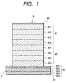
- Fig. 1 illustrates a cross-sectional view of the layer structure of a piezoelectric device according to Embodiment 1, as viewed at a cross section taken along A-A in Fig. 4.
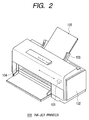
- Fig. 2 illustrates a perspective view of an ink-jet printer that uses the present invention.
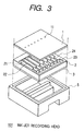
- Fig. 3 illustrates an exploded perspective view of an ink-jet recording head according to the present invention.
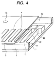
- Fig. 4 illustrates a partial cross-sectional, perspective view of a pressure chamber substrate of an ink-jet recording head according to the present invention.
- Fig. 5 illustrates a cross-sectional view for explaining an operating principle for an ink-jet recording head according to the present invention, as viewed at a cross-section taken along A-A in Fig. 4.
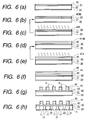
- Fig. 6 illustrates cross-sectional views of a structure formed during a method for manufacturing an ink-jet recording head according to the present invention.
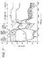
- Fig. 7 illustrates a graph for the composition distribution of an ink-jet recording head according to the embodiment of the present invention, with the sputtering period of time along the vertical axis corresponding to the depth from the surface of a piezoelectric layer in the direction of the thickness.
- Fig. 8 illustrates a cross-sectional view for explaining the layer structure of a piezoelectric device according to Embodiment 2, as viewed at a cross section taken along A-A in Fig. 4.
- Fig. 9 illustrates a cross-sectional view for explaining the layer structure of a piezoelectric device according to Embodiment 3, as viewed at a cross section taken along A-A in Fig. 4.
- Fig. 10 illustrates a cross-sectional view for explaining the layer structure of a piezoelectric device according to Embodiment 4, as viewed at a cross section taken along A-A in Fig. 4.
- Fig. 11 illustrates a cross-sectional view for explaining the layer structure of a piezoelectric device according to Embodiment 5, as viewed at a cross section taken along A-A in Fig. 4.
- Fig. 12 illustrates a cross-sectional view for explaining a modification of the layer structure of a piezoelectric device according to Embodiment 5, as viewed at a cross section taken along A-A in Fig. 4.
- an ink-jet printer 100 that is pertinent to the present invention comprises an ink-jet recording head 101 of the present invention, a main body 102 and a tray 103.
- the ink-jet recording head 101 is driven in a direction indicated by an arrow, and ejects ink droplets through its nozzles 11 (see Fig. 3) onto the sheet 105 to enable printing.
- the main body 102 which includes the tray 103, holds internally the ink-jet recording head 101 that is to be driven.
- print data are transmitted from a computer (not shown)
- the sheet 105 fed along the tray 103 is delivered to a discharge port 104.
- the tray 103 is so designed that a sheet 105 which is mounted on it is supplied to the interior of the main body 102.
- the ink-jet recording head 101 is constituted by a nozzle plate 1, a pressure chamber substrate 2, a vibration plate 3 and a housing 5.
- the nozzle plate 1 is attached to the pressure chamber substrate 2, so that nozzles are located at positions corresponding to those of a plurality of cavities (pressure chambers) 21 formed on the pressure chamber substrate 2.
- the pressure chamber substrate 2 includes the cavities 21, side walls 22, a reservoir 23 and supply ports 24.
- the cavities 21 are formed by etching the substrate, which is made of silicon, the side walls 22 serve as partitions for the cavities 21, and the reservoir 23 serves as a flowpath used in common along which ink can be supplied after the cavities 21 are filled with ink.
- the supply ports 24 are so formed that ink can be introduced along them to the cavities 21.
- the housing 5 is made of a resin or metal to hold the pressure chamber substrate 2, to which the nozzle plate 1 and the vibration plate 3 are attached. Ink is supplied to the housing 5 from an ink tank (not shown) and to the pressure chamber substrate 2 through an ink tank port 33 shown in Fig. 4.
- the vibration plate 3 can be attached to one face of the pressure chamber substrate 2, as is shown in Fig. 4. Piezoelectric devices 4 having a predetermined shape are formed on the vibration plate 3.
- the layer structure of the vibration plate 3 and the piezoelectric devices 4 (cross section taken along A-A in Fig. 4) includes an upper electrode film 40 as a piezoelectric device 4, a first piezoelectric layer 41, a second piezoelectric layer 42, a lower electrode film 30, which serves as the vibration plate 3, and an insulating film 31.
- the upper electrode film 40 serves as an electrode for applying a voltage to the piezoelectric layer, and is made of a conductive material, such as platinum (Pt), 0.1 ⁇ m thick.
- the first piezoelectric layer 41 is constituted by a plurality of layers, e.g., four ceramic layers 411 to 414.
- the individual ceramic layers are polarized by being individually dried and pyrolyzed.
- the ceramic layers 411 to 414 are composed of a piezoelectric ceramic composition that has a comparatively large dielectric constant.
- the first piezoelectric layer 41 be a perovskite structure crystal that is represented by the general formula: Pb(Zr (1-y) Ti y ) (1-z) (b (1-x) b' x ) z O 3 where b and b' are divalent to hexavalent metal elements, and x is a real number of 0 ⁇ x ⁇ 1, y is a real number of 0 ⁇ y ⁇ 1 and z is a real number of 0 ⁇ z ⁇ 1.
- Equation (2) means that the elements are electrically neutral.
- the divalent to hexavalent metal elements are, for example, Mg, Sc, Cr, Mn, Fe, Co, Ni, Zn, Nb, Cd, In, Sn, Sb, La, Yb, Lu, Ta, W and Bi.
- the composition as it relates to b and b' of the first piezoelectric layer 41 is, for example, Pb(Ni 1/3 Nb 2/3 )O 3 , Pb(Mg 1/3 Ta 2/3 )O 3 , Pb(Zn 1/3 Nb 2/3 )O 3 , Pb(Co 1/3 Nb 2/3 )O 3 , Pb(Mn 1/2 W 1/2 )O 3 , Pb(Zn 1/2 W 1/2 )O 3 , Pb(Mg 1/2 W 1/2 )O 3 , Pb(Co 1/2 W 1/2 )O 3 , Pb(Ni 1/2 W 1/2 )O 3 or Pb(Fe 2/3 W 1/3 )O 3 .
- the typical composition, of the first piezoelectric layer, that exhibits a preferable piezoelectric characteristic is Pb(Zr 0.56 Ti 0.44 ) 0.8 (Mg 1/3 Nb 2/3 ) 0.2 O 3 .
- the composition for the first piezoelectric layer may not include Mg.
- the dielectric constant ⁇ which is proportional to the piezoelectric characteristic d, is increased, so that the piezoelectric characteristic d is enhanced.
- the third element is distributed more uniformly in the direction of the depth, so that the voltage withstandability and the durability of the piezoelectric layer are improved.
- the piezoelectric ceramic (hereinafter referred to as a "precursor") immediately after it is coated is amorphous, and an element diffusion phenomenon occurs on a face that contacts another composition (e.g., the second piezoelectric layer).
- the second piezoelectric layer 421 since the second piezoelectric layer 421 has been dried, pyrolyzed and crystallized, and a ceramic layer 414b has also been crystallized as the result of a drying and pyrolyzing process after it was coated, a diffusion phenomenon rarely occurs between the precursor and the second piezoelectric layer. Therefore, the compositions of at least the ceramic layers 411 to 413 are maintained as they have been coated.
- the second piezoelectric layer 42 consists of a plurality of layers, e.g., four ceramic layers 421 to 424.
- the individual ceramic layers are crystallized by drying and pyrolyzing each layer as it is formed.
- the ceramic layers 421 to 424 have a piezoelectric ceramic composition that has a comparatively high piezoelectric constant g.
- Such a composition is, for example, the one containing an oxide (PZT: lead zirconate titanate) of lead (Pb), zirconium (Zr) and titanium (Ti).
- PZT lead zirconate titanate
- Ti titanium
- a ceramic layer precursor 422b in the second piezoelectric layer 42 is amorphous immediately after it is coated, and an element diffusion phenomenon occurs on a face that contacts another composition (e.g., a titanium layer 301 in the lower electrode film 30).
- another composition e.g., a titanium layer 301 in the lower electrode film 30.
- the ceramic layer 424b that is coated is dried, pyrolyzed and crystallized, a diffusion phenomenon rarely occurs between the precursor 424b and the composition of the lower electrode film 30. Therefore, the compositions at least of the ceramic layers 421 to 423 are maintained as they have been coated.
- the piezoelectric layer 424 that directly contacts the lower electrode film 30 is a layer wherein crystal first grows.
- a crystal nucleus be included in the piezoelectric film precursor that is applied for the formation of the piezoelectric layer.
- the perovskite structure grows from the phase boundary of the crystal nucleus.
- the crystal growth continues in consonance with the crystal structure of a piezoelectric layer with which in contact. That is, it is preferable that a crystal nucleus exist in a layer at least that contacts the lower electrode film in order to form a piezoelectric device having a satisfactory crystal structure.
- the first piezoelectric layer 41 and the second piezoelectric layer 42 may be laminated in the reverse order. Specifically, the first piezoelectric layer 41 may be formed on the lower electrode film 30, the second piezoelectric layer 42 may be formed thereon, and then the upper electrode film 40 may be formed thereon.
- These piezoelectric layers may be constituted by either more than or fewer than four layers. It should be noted that when too many layers are laminated, the drive voltage will be raised and the advantage of the present invention will be lost. When there are too few layers laminated, the uniformity of the compositions due to the diffusion phenomenon is accelerated between the two piezoelectric layers, so that the resultant structure of the piezoelectric device would be the same as that consisting of a single composition, and an increase in the piezoelectric constant d could not be expected. Further, if each ceramic layer is too thick, the thickness of the entire layer lamination is increased accordingly, and a higher drive voltage will be required.
- each ceramic layer is formed too thin, the thicknesses of the layers will not be uniform, so that the characteristics of the individual piezoelectric devices that are separated by etching will be varied, the number of fabrication steps will be increased and the manufacturing costs will be raised.
- two to six ceramic layers are laminated for each piezoelectric layer, and more preferably, four layers. It is preferable that the thickness of each ceramic layer be 80 nm to 200 nm, and more preferably, 125 nm.
- each piezoelectric layer need not have the same thickness. For example, only layers (414 and 424) that contact other compositions may be formed thin; the other layers may be thick. In this manner, the thickness of the layer through which the diffusion of compositions will occur can be reduced.
- the lower electrode film 30 is paired with the upper electrode film 40 to apply a voltage to the piezoelectric layers, and is formed by laminating conductive materials, such as a titanium (Ti) layer 301, a platinum (Pt) layer 302 and a titanium (Ti) layer 303. Further, in order to improve the contact between the lower electrode film 30, which includes the titanium layer 301, the platinum layer 302 and the titanium layer 303, and the insulating film 31, a titanium oxide layer 304 and a titanium layer 305 are inserted between the lower electrode film 30 and the insulating film 31.
- conductive materials such as a titanium (Ti) layer 301, a platinum (Pt) layer 302 and a titanium (Ti) layer 303.
- the insulating film 31 is made of non-conductive material, such as silicon dioxide, which is formed by thermal oxidation of a silicon substrate.
- the insulating film 31 can be deformed, as the piezoelectric layer is displaced in the direction of thickness and the perpendicular direction, and momentarily increases the pressure inside the cavities 21.
- a piezoelectric constant d is provided as an index for the characteristic of a piezoelectric device, and is represented by the unit C/N, i.e., by the quantity of electric charges that are generated upon the application of a pressure of 1 newton.
- the piezoelectric constant d correlates with a product of piezoelectric constant g, which is a factor of proportionality derived from an electric field and stress, and a dielectric constant, which is a factor of proportionality derived from an electric field and a face charge density.
- the piezoelectric constant d of the entire structure is proportional to the product of the relatively large piezoelectric constant g and the relatively large dielectric constant. This is because the structure of the piezoelectric device can be analyzed by using a capacitor arrangement model and a mechanical arrangement model.
- the piezoelectric constant d when the piezoelectric constants g of the two layers differ can be understood through observation of the atomic structure. When piezoelectric layers having different compositions are formed in contact, crystal of one of the piezoelectric layer epitaxially grows and this growth is transmitted to the other piezoelectric layer.
- a piezoelectric constant g is obtained that differs from that obtained when the piezoelectric ceramic material is formed of single crystal. Since the piezoelectric layer that has the small piezoelectric constant g is affected by the piezoelectric layer having the large constant g, the piezoelectric constant g at the piezoelectric layer having the small constant g can be increased.
- a piezoelectric device that is a laminate of two piezoelectric layers having different dielectric constants has a dielectric characteristic that is similar to that obtained by a series connection of capacitors that have different dielectric constants and have a smaller gap than a gap at single type of layers.
- the dielectric constant of the total piezoelectric layer is a value lying midway between the values of the dielectric constants of the two piezoelectric layers. In other words, the dielectric constant of the entire device can be increased by laminating layers having large dielectric constants.
- the second piezoelectric layer 42 is formed of PZT, its piezoelectric constant g is large.
- the first piezoelectric layer 41 which contains magnesium (Mg) and niobium (Nb) in addition to PZT has a slightly smaller piezoelectric constant g and a larger dielectric constant than has the second piezoelectric layer 42.
- the obtained piezoelectric constant d is higher than is that of a piezoelectric device constituted by either piezoelectric layer alone. Therefore, the piezoelectric device in this embodiment has a larger piezoelectric constant d than has a conventional piezoelectric device composed of one composition, and is displaced more upon the application of the same voltage as is the conventional device.
- Fig. 5 is a cross-sectional view of two cavities of the ink-jet recording head according to the present invention.
- a voltage V0 is applied to a piezoelectric device 4A corresponding to a cavity 21A
- a voltage V1 is applied to a piezoelectric device 4B corresponding to a cavity 21B.
- the voltage V0 is a voltage level (e.g., 0 V) at which there is no displacement of the piezoelectric device
- the voltage V1 is a voltage level (e.g., 15 V) at which there is a displacement of the piezoelectric device.
- Vibration plate formation step (Fig. 6(a)): First, an insulating film 31 and a lower electrode 30, which serve as vibration plate films 3, are formed on a silicon substrate 20.
- the silicon substrate 20 is thermally oxidized in a dry oxygen atmosphere for 22 hours in a furnace at 1100°C, and in this manner a thermal oxide film of approximately 1 ⁇ m thick is formed as the insulating film 31 on the silicon substrate 20.
- the silicon substrate 20 may be thermally oxidized in an oxygen and water vapor atmosphere for five hours to form the approximately 1 ⁇ m thick thermal oxide film.
- the insulating film 31 obtained by either of these methods is used both for electric insulation and also as a protective layer for an etching process.
- a titanium layer 305 of approximately 20 nm, a titanium oxide layer 304 of approximately 20 nm, a titanium layer 303 of approximately 5 nm, a platinum layer 302 of approximately 500 nm and a titanium layer 301 of approximately 5 nm are laminated sequentially employing the direct current sputtering method.
- a platinum layer approximately 800 nm thick may be formed by using the sputtering method. It should be noted that the titanium layer 303 under the platinum layer 302 is necessary.
- Second piezoelectric layer formation step (Fig. 6(b) and (c)): The second piezoelectric layer 42 is formed.
- the above steps i) and ii) are repeated to form a ceramic layer 423 on the ceramic layer 424, and the steps i) and ii) are repeated two more times to form ceramic layers 422 and 421.
- the coating, drying and pyrolyzing steps are repeated at predetermined number of times, e.g., four times.
- metal alkoxide is hydrolyzed or polycondensated, thereby forming a metal-oxygen-metal network.
- the lamination is thermally processed in a specific atmosphere.
- a specific atmosphere for example, in an oxygen atmosphere, the laminate is heated for five minutes at 600°C and further for one minute at 725°C during a rapid thermal annealing process (RTA).
- RTA rapid thermal annealing process
- First piezoelectric layer formation step (Fig. 6(d) and (e)): A first piezoelectric layer 41 is formed on the second piezoelectric layer 42 formed at the above step.
- the resultant structure is thermally processed at a predetermined atmosphere to accelerate the crystallization of the ceramic layers and to enhance the characteristic of the piezoelectric layer.
- a predetermined atmosphere for example, in an oxygen atmosphere, the laminated structure is heated for five minutes at 650°C and then for one minute at 900°C during the rapid thermal annealing process (RTA) using oxygen.
- RTA rapid thermal annealing process
- Upper electrode formation step (Fig. 6(f)): An upper electrode film 40 is formed on the first piezoelectric layer 41 using either the electron beam vacuum evaporation method or the sputtering method. Aluminum or platinum is used as the upper electrode material, and the thickness of the material is approximately 100 nm. h
- Etching step (Fig. 6(g): After the individual layers have been formed, the laminated structure on the vibration plate film 3 is masked to correspond to the shapes of the cavities, and etching of the surrounding surface is performed to remove the upper electrode film and the piezoelectric layers. That is, a resist layer having a uniform thickness is applied to the laminated structure using either the spinner method or the spray method, and the resultant structure is exposed and developed to form the resist layer on the upper electrode film 40. Then, unnecessary portions of the layer are removed either by ion-milling or by dry etching, which is the procedure that is normally employed. As a result, by following the above described steps, piezoelectric devices can be provided.
- Pressure chamber formation and nozzle plate installation step (Fig. 6(h)): A cavity 21 is formed in the other face of the pressure chamber substrate 2.
- the etching to provide the cavity space is performed, for example, by anisotropic etching, using an active gas, such as parallel-plate reactive ion etching.
- the portions remaining after the etching is completed serve as side walls 22.
- Nozzle plates 1 are aligned and bonded, using resin, to the pressure chamber substrate 2 that has been etched, so that the positions of the nozzles 11 correspond to the locations of the cavities 21 in the pressure chamber substrate 2.
- the pressure chamber substrate 2 to which the nozzle plates 1 are bonded is attached to the housing 5. In this fashion, the ink-jet recording head 101 can be completed.
- the ink-jet recording head 101 was acquired by employing the above described manufacturing method.
- Pb(Zr 0.56 Ti 0.44 ) 0.8 (Mg 1/3 Nb 2/3 ) 0.2 O 3 was employed as the composition for the first piezoelectric layer
- PbZr 0.56 Ti 0.44 O 3 was employed as the composition for the second piezoelectric layer.
- the magnesium Mg content and the niobium Nb content of the first piezoelectric layer are increased compared with those of the second piezoelectric layer. It is understood that ion diffusion was protected and the original compositions of the two piezoelectric layers were maintained. This is because each piezoelectric layer is constituted by four layers.
- the thickness of the first piezoelectric layer was 500 nm, and the thickness of the second piezoelectric layer was also 500 nm. When the smoothness on the surface was evaluated by an SEM (scanning electron microscope), it was 30 nm to 100 nm.
- Table 1 shows the results obtained from the comparison of the piezoelectric constants d, the piezoelectric constants g and the dielectric constants for the ink-jet recording head in this example, for a piezoelectric device that was formed with the same thickness as the ink-jet recording head of this example by using the composition employed for the first piezoelectric layer, and for a piezoelectric device that was formed with the same thickness as the ink-jet recording head of this example by using the composition employed for the second piezoelectric layer.
- Subscript 31 in Table 1 indicates a value in the direction of the thickness of the piezoelectric device.
- the piezoelectric device in this embodiment which is constituted by a lamination of the two types of piezoelectric layers, has a comparatively large piezoelectric constant g and dielectric constant, and accordingly, the large piezoelectric constant d is obtained.
- Example 2 of the present invention the effect of Mg on the first piezoelectric layer was examined.
- Table 2 shows the piezoelectric characteristic, as well as the voltage withstandability and the durability, of a piezoelectric device that is formed with a material having the composition shown in equations (1) and (2), instead of the composition used for the first piezoelectric layer in example 1.
- the piezoelectric characteristic of a piezoelectric device that is formed as a single layer is also shown for the comparison.
- Piezoelectric device type Composition (first piezoelectric layer) Piezoelectric constant d31[pC/N] Voltage with standability [V/ ⁇ m] Durability Piezoelectric device in Embodiment Pb (Zr 0.56 Ti 0.44 ) 0.8 (Ni 1/3 Nb 2/3 ) 0.2 O 3 170 80 1.2 Ordinary piezoelectric device Pb (Zr 0.56 ti 0.44 ) 0.8 (Mg 1/3 Nb 2/3 ) 0.2 O 3 150 70 1.0
- a large piezoelectric constant d can be obtained by laminating a plurality of types of piezoelectric layers, and a piezoelectric device can be produced that can be displaced more than in the conventional case upon the application of the same voltage. Therefore, an ink-jet recording head can be provided that, upon the application of the same voltage, can eject a larger quantity of ink droplets at a higher speed than is possible in the conventional case.
- each ceramic layer of the piezoelectric layer is crystallized, a diffusion phenomenon can be prevented, even for an amorphous ceramic material, and a layer structure that can maintain a large piezoelectric constant d can be provided.
- the dielectric constant of the piezoelectric device as a whole can be increased by using a specific composition for one of piezoelectric layers. Especially when a composition that does not include Mg is employed for a piezoelectric layer, a piezoelectric device can be provided that has superior voltage withstandability, as well as a large piezoelectric constant d.
- Embodiment 2 While the thicknesses of the first and the second piezoelectric layers are the same in Embodiment 1, in Embodiment 2 a new application is provided by changing the thicknesses of the two.
- the layer structure of the piezoelectric device 4b in this embodiment (cross section taken along A-A in Fig. 4) includes an upper electrode film 40 and ceramic layers 431 and 438, as is shown in Fig. 8.
- the upper electrode film 40 which is one of the electrodes provided to apply a voltage to the piezoelectric layer, is formed of a conductive layer, such as a 0.1 ⁇ m thick platinum (Pt), as in Embodiment 1.
- the ceramic layers 431 to 438 are sorted into a first piezoelectric layer 41 and a second piezoelectric layer 42, as in Embodiment 1. However, the boundary between the two layers is arbitrarily changed from between the second layer 432 and the third layer 433 to between the sixth layer 436 and the seventh layer 437.
- the thickness of each ceramic layer is 125 nm, as in Embodiment 1.
- the ceramic layers allocated for the first piezoelectric layer 41 have a piezoelectric ceramic composition that has a comparatively high dielectic constant, and the same composition as in Embodiment 1 can be employed.
- An example composition for the first piezoelectric layer is Pb(Zr 0.56 Ti 0.44 ) 0.8 (Mg 1/3 Nb 2/3 ) 0.2 O 3 .
- the ceramic layers allocated for the second piezoelectric layer 42 have a piezoelectric ceramic composition that has a comparatively small dielectic constant and a comparatively high piezoelectric constant g, and the same composition as in Embodiment 1 can be employed.
- An example composition for the second piezoelectric layer is PbZr 0.56 Ti 0.44 O 3 .
- a crystal nucleus exist in at least the layer that contacts a lower electrode film in order to form a piezoelectric device having a satisfactory crystal structure.
- a vibration plate film 3 is constituted by a lower electrode film 30 and an insulating film 31, and since the specific structure is the same as that in Embodiment 1, no further explanation for it will be given.
- the first piezoelectric layer 41 and the second piezoelectric layer 42 may be laminated in the reverse order. That is, the first piezoelectric layer 41 may be formed on the lower electrode film 30, the second piezoelectric layer 42 be formed thereon, and finally an upper electrode film 40 be formed atop the two.
- the method used for manufacturing a piezoelectric device in Embodiment 2 is substantially the same as that in Embodiment 1, except as regards the number of laminated layers in each piezoelectric layer.
- the vibration plate film step (Fig. 6(a))
- the insulating film 31 and the lower electrode film 30, which serve as the vibration plate film 3 are formed on a silicon substrate 20, and the second piezoelectric layer 42 is formed at the second piezoelectric layer formation step (Fig. 6(b) and (c)).
- the number of ceramic layers to be laminated is changed, as needed.
- the number of ceramic layers to be laminated is adjusted by changing the ratio of the thicknesses of the two piezoelectric layers so that the entire piezoelectric device has a desired piezoelectric constant g, or a desired dielectric constant. Specifically, when the first piezoelectric layer has the piezoelectric constant g1 and the second piezoelectric layer has the piezoelectric constant g2 (g2 > g1), the ratio of the thicknesses of the two piezoelectric layers is adjusted to obtain a desired piezoelectric constant g (g2 > g > g1).
- the number of the ceramic layers in each piezoelectric layer is adjusted to obtain a desired dielectric constant ⁇ ( ⁇ 1 > ⁇ > ⁇ 2).
- the ratio of the thicknesses of the first and the second piezoelectric layers can be adjusted by changing the thicknesses of the ceramic layers. The total number of ceramic layers in the first and the second piezoelectric layers should not exceed 12 because when too many layers are laminated, the drive voltage must be increased.
- the individual ceramic layers are formed applying a coat of the above described piezoelectric ceramic material at the coating step (Fig. 6(b)), and by drying and pyrolyzing the thus applied ceramic layers at the drying and degreasing step (Fig. 6(c)).
- the rapid thermal annealing process is performed in the same manner.
- the timing for the performance of the rapid thermal annealing process is determined in consonance with the number of laminated layers in a piezoelectric layer.
- the first rapid thermal annealing process is performed when half of the ceramic layers have been laminated. For the first rapid thermal annealing process, in an oxygen atmosphere the ceramic layers are heated for five minutes at 600°C and then for one minute at 725°C.
- the first piezoelectric layer 41 is formed on the second piezoelectric layer 42 at the first ceramic layer formation step (Fig. 6(d) and (e)).
- the ceramic layers of the first piezoelectric layer are formed by applying a coat of the piezoelectric ceramic material and by drying and degreasing it, in the same manner as for the second piezoelectric layer.
- the final rapid thermal annealing process is performed one time. In this process, in an oxygen atmosphere the ceramic layers are heated, for example, for five minutes at 650°C and then for one minute at 900°C.
- the upper electrode film 20 is formed on the first piezoelectric layer 41 at the upper electrode formation step (Fig. 6(f)).
- the layer portions are removed at the etching step (Fig. 6(g)), so that the shapes of the piezoelectric devices correspond to those of the cavities.
- the piezoelectric device 4b can be completed.
- cavities 21 are formed in the other face of the pressure chamber substrate 2, which is then bonded to a nozzle plate.
- the piezoelectric constant g and the dielectric constant of the layer lamination are values lying midway between the values for the piezoelectric constants g and the values for the dielectric constants of the individual layers. Since the piezoelectric constant g and the dielectric constant of the layer lamination are changed in accordance with the ratio of the thicknesses of the two layers, the thicknesses of the two piezoelectric layers can be changed to obtain a desired piezoelectric constant g and a desired dielectric constant.
- the piezoelectric constant g is a value lying midway between the values of the piezoelectric constants g of the two layers can be understood from the observation at the atomic structure level, as in Embodiment 1. Since the dielectric constant for the entire piezoelectric device is changed depending on the ratio of the thicknesses of the two layers, the thicknesses of the two layers can be changed in order to obtain a desired dielectric constant.
- the number of layers to be laminated can be changed in accordance with the limit value, so that a piezoelectric device can be provided for which the piezoelectric constant d is increased, and either the piezoelectric constant g or the dielectric constant is reduced. Since it is preferable that a circuit current be reduced, for example, for an actuator that reads a signal from a compact disk, the dielectric constant must be reduced for a piezoelectric device for such an actuator. In this case, the dielectric constant of a piezoelectric device that provides a desired circuit current need only be calculated so as to constitute a piezoelectric device that has a dielectric constant that is equal to or lower than the obtained dielectric constant.
- the first and the second piezoelectric layers 41 and 42 must be designed to be equivalent to the thickness of two-layers, i.e., about 250 nm.
- Table 3 shows piezoelectric constant d 31 (piezoelectric characteristic d in the direction of the depth), piezoelectric constant g 31 (piezoelectric characteristic g in the direction of the depth), and a dielectric constant obtained when the numbers of layers were changed for the first piezoelectric layer and for the second piezoelectric layer of a piezoelectric device that includes the total eight layers.
- the same composition as in Example 1 in Embodiment 1 was employed.
- Second piezoelectric layer count Piezoelectric constant d d31[pC/N] Piezoelectric constant j g31[m ⁇ mV/N] Piezoelectric constant e 2 6 175 15.2 1300 3 6 175 14.5 1370 4 4 180 14.0 1450 5 3 180 13.5 1530 6 2 185 13.0 1620
- Embodiment 2 the effects obtained in Embodiment 1 are also acquired in Embodiment 2.
- the thicknesses of the first and the second piezoelectric layers are changed so that the dielectric constant and the piezoelectric constant g can be restricted to desired values, and so that a large piezoelectric constant d can be maintained for a piezoelectric device.
- Embodiment 3 only one layer is provided for each of the first piezoelectric layer and the second piezoelectric layer in above described embodiments, and a further, third piezoelectric layer is formed to provide a variation of the above layer structure.
- Fig. 9 is a cross-sectional view of a piezoelectric device 4c according to this embodiment.
- the piezoelectric device 4c including a vibration plate 3 and a pressure chamber substrate 2, is cut in the direction of the width. Since an ink-jet printer (see Fig. 2) and an ink-jet recording head (see Figs. 3 and 4), for which the piezoelectric device 4c is to be used, is the same as those in Embodiment 1, no explanation for them will be given.
- the piezoelectric device in Embodiment 3 includes three or more types of piezoelectric layers.
- the piezoelectric layer that has the largest dielectric constant of the three is called a first piezoelectric layer
- the piezoelectric layer that has the largest piezoelectric constant g is called a second piezoelectric layer
- the other piezoelectric layers being generally called third piezoelectric layers. Therefore, the third piezoelectric layers can consist of a plurality of types of layers.
- Fig. 9 in the layer structure (cross section taken along A-A in Fig. 4) of the piezoelectric device 4c in this embodiment, three or more types (six types in Fig. 9) of piezoelectric layers 41 to 46 are located between an upper electrode film 40 and a vibration plate 3.
- the piezoelectric layers 41 to 46 have different compositions. For them, the compositions employed for the first and the second piezoelectric layers specifically explained in Embodiment 1 are employed. Assume that a layer denoted by 41, the same numeral as in Embodiment 1, is a first piezoelectric layer, and a layer denoted by numeral 42 is a second piezoelectric layer. The other layers, i.e., the third piezoelectric layers 43 to 46, are laminated in order to increase the dielectric constant, to increase the piezoelectric constant g, or for another purpose, such as the reduction of the internal stress of the piezoelectric layer.
- the composition represented by equation (1) or (2) in Embodiment 1 is used for the first piezoelectric layer 41, PZT is used for the second piezoelectric layer 42, and a mixture of the compositions represented by equations (1) and (2) is used for the third piezoelectric layers 43 to 46.
- the composition obtained by, for example, changing metal elements b and b' in equations (1) and (2) is employed for each of the third piezoelectric layers 43 to 46.
- each of the piezoelectric layers 41 to 46 be constituted by laminating a plurality of ceramic layers based on the same idea, as in Embodiment 1. This is because when a thick layer is formed, a crack occurs and a layer having a satisfactory crystal structure can not be formed. For the same reason as in Embodiment 1, it is preferable that a crystal nucleus exist in at least the layer that contacts the lower electrode film in order to form a piezoelectric device having a satisfactory crystal structure.
- the order for the layer lamination is not limited to that shown in Fig. 9, and can be variously changed.
- the number of third piezoelectric layers 43 to 46 is not limited to four; an arbitrary number of layers (43 to 4n (n is a natural numbers) can be formed.
- the first and the second piezoelectric layers 41 and 42 need not contact each other.
- the thicknesses of the individual piezoelectric layers and the number of laminated ceramic layers need not be the same, and can be variously altered in consonance with the objects of the individual layers. For example, when the dielectric constant is to strongly affect the entire structure, the thickness of the first piezoelectric layer 41 and the number of laminated ceramic layers are increased. When the piezoelectric constant g is to greatly effect the entire structure, the thickness of the second piezoelectric layer 42 and the number of laminated ceramic layers are increased.
- the piezoelectric constant d can be increased. Specifically, when the dielectric constants of the piezoelectric layers 41 to 4n are ⁇ 1 to ⁇ n , ⁇ 1 > ⁇ 2 to ⁇ n , and when the piezoelectric constants g of the piezoelectric layers 41 to 4n are g 1 to g n , g 2 > g 1 and g 3 to g n .
- the piezoelectric constant d in the direction of the thickness of the piezoelectric device is represented as d ⁇ g x ⁇ x ⁇ 0 , i.e., the above equation (3).
- the smallest constant among g 1 and g 3 to g n ⁇ g ⁇ g 2 , and the smallest constant among ⁇ 2 to ⁇ n ⁇ ⁇ ⁇ ⁇ 1 , where ⁇ 0 is a dielectric constant in vacuum ( 8.85 x 10 -12 [F/m]).
- the dielectric constant of the entire piezoelectric device can be increased.
- the effect of the dielectric layer is greater when the thicker layer is formed, as is described above.
- the large piezoelectric constants g of the piezoelectric layers are set, even though one piezoelectric layer has a low piezoelectric constant g the dielectric constant g of the entire piezoelectric device can be increased.
- the dielectric constant g In order to increase the dielectric constant and the piezoelectric constant g, only the thicknesses of the piezoelectric layers that have large dielectric constants and piezoelectric constants g and the number of ceramic layers need be increased.
- Embodiment 3 provided is a piezoelectric device that has three or more types of piezoelectric layers and with which the same effects can be acquired as in Embodiment 1.
- the layer structure in this embodiment can be applied especially when layers are to be laminated that have low dielectric constants and piezoelectric constants g but possess other advantages.
- a variation of the layer structure includes a plurality of first piezoelectric layers and a plurality of second piezoelectric layers.
- Fig. 10 is a cross-sectional view of a piezoelectric device according to this embodiment.
- the piezoelectric device 4d including a vibration plate 3 and a pressure chamber substrate 2 is cut in the direction of the width.
- An ink-jet printer (see Fig. 2) and an ink-jet recording head (see Figs. 3 and 4), for which the piezoelectric device 4d is employed, have the same structure as in Embodiment 1, and no explanation for them will be given.
- the piezoelectric device 4d (cross section taken along A-A in Fig. 4) in Embodiment 4 is formed by alternately laminating the first piezoelectric layer 41 and the second piezoelectric layer 42 in Embodiment 1 a plurality of times. Since its specific composition is the same as that in Embodiment 1, no explanation for it will be given.
- the piezoelectric layers 41 and 42 be formed by laminating a plurality of ceramic layers, based on the same idea as that in Embodiment 1. This is because when a thick layer is formed, a crack occurs and a layer having a satisfactory crystal structure can not be formed. For the same reason as in Embodiment 1, it is preferable that a crystal nucleus be present at least in a layer that contacts the lower electrode film in order to form a piezoelectric device having a satisfactory crystal structure.
- the order for the lamination is not limited to that shown in Fig. 10, and can be variously changed.
- the positions of the first piezoelectric layer 41 and the second piezoelectric layer 42 may be reversed.
- neither the thicknesses of the individual piezoelectric layers nor the number of laminated ceramic layers need be the same; they can be variously altered as needed.
- the dielectric constant is to strongly affect the entire structure
- the thickness of the first piezoelectric layer 41 and the number of laminated ceramic layers are increased.
- the piezoelectric constant g is to greatly affect the entire structure, the thickness of the second piezoelectric layer 42 and the number of laminated ceramic layers are increased.
- the piezoelectric constant d can be increased.
- the dielectric constants of the individual piezoelectric layers are the same as the dielectric constant of a piezoelectric layer that has a thickness equivalent to the total thickness of the individual piezoelectric layers. This is because, since the piezoelectric device is a series connection of capacitors, even when their positions are changed, the dielectric constant of the piezoelectric device is not altered.
- the piezoelectric constant g can be larger than that in Embodiment 1. As is described above, since the stress in the second piezoelectric layer, which has a larger piezoelectric constant g, affects the crystal structure of the first piezoelectric layer, which has a smaller piezoelectric constant g, in this embodiment the piezoelectric constant g of the entire piezoelectric device is increased.
- Embodiment 4 provided is a piezoelectric device that is formed by alternately laminating the first and the second piezoelectric layers and that can provide the same effect as that in Embodiment 1. Especially in this embodiment, the effect of the piezoelectric constant g can be increased.
- Embodiment 5 is provided a variation of the layer structure, such as a alternate lamination structure using the third piezoelectric layer explained in Embodiment 3.
- Fig. 11 is a cross-sectional view of a piezoelectric device 4e according to this embodiment.
- the piezoelectric device including a vibration plate 3 and a pressure chamber substrate 2 is cut in the direction of the width.
- An ink-jet printer (see Fig. 2) and an ink-jet recording head (see Figs. 3 and 4), for which the piezoelectric device 4e is employed, have the same structure as in Embodiment 1, and no explanation for them will be given.
- the piezoelectric device 4e in Embodiment 5 (cross section taken along A-A in Fig. 4) is constructed by laminating, a plurality of times, a layer structure that includes the first piezoelectric layer 41 and the second piezoelectric layer 42 in Embodiment 4, and the third piezoelectric layer 43 in Embodiment 3.
- a plurality of types of third piezoelectric layers 43 to 4n may be repeated as explained in Fig. 9. Since specific compositions are the same as those in Embodiments 1 and 3, no explanation for them will be given.
- the piezoelectric layers 41 to 43 be formed by laminating a plurality of ceramic layers, based on the same idea as in Embodiment 1. This is because when a thick layer is formed, a crack occurs and a layer having a satisfactory crystal structure can not be formed. Further, for the same reason as in Embodiment 1, it is preferable that a crystal nucleus be present at least in the layer that contacts the lower electrode film in order to form a piezoelectric device having a satisfactory crystal structure.
- the order for the layer lamination is not limited to that shown in Fig. 11, and can be variously changed.
- the relative positions of two of the first, the second and the third piezoelectric layers 41, 42 and 43 may be reversed.
- a piezoelectric device 4f wherein the order in which the piezoelectric layers 41, 42 and 43 are laminated irregular may be employed.
- the number of piezoelectric layers of a specific type may differ from the numbers of the other types of piezoelectric layers. And neither the thicknesses of the individual piezoelectric layers nor the number of laminated ceramic layers need be the same; they can be variously altered as needed.
- the dielectric constant when the dielectric constant is to strongly affect the entire structure, the number of first piezoelectric layers 41, the thickness of each layer and the number of laminated ceramic layers are increased.
- the piezoelectric constant g is to greatly effect the entire structure, the number of second piezoelectric layers 42, the thickness of each layer and the number of laminated ceramic layers are increased.
- the thus structured piezoelectric devices 4e and 4f have a large dielectric constant and a large piezoelectric constant g, their piezoelectric constants d can be increased. Therefore, if the large dielectric constants of the piezoelectric layers are set, even though one piezoelectric layer has a low dielectric constant the dielectric constant of the entire piezoelectric device can be increased. The effect of the dielectric layer is greater when a thicker layer is formed, as is described above.
- the dielectric constant g of the entire piezoelectric device can be increased.
- the dielectric constant g In order to increase the dielectric constant and the piezoelectric constant g, only the number of piezoelectric layers that have large dielectric constants and large piezoelectric constants g, the thickness of each layer, and the number of ceramic layers need be increased. Particularly, the same action as in Embodiment 4 affects on the piezoelectric constant g, which can provide mechanical effects for the first piezoelectric layer.
- a piezoelectric device wherein one or more of piezoelectric layers of three or more types are laminated at arbitrary locations to acquire the same effect as that in the above described embodiments.
- the piezoelectric characteristic of the piezoelectric device can be adjusted by employing the functions of the individual piezoelectric layers and the idea incorporated in this embodiment.
- the layer structures in the embodiments are also merely examples, and various other layer structures can be devised.
- a piezoelectric device when a piezoelectric device is constituted by a plurality of compositions, and when an arrangement includes a layer having a large dielectric constant and a layer having a high piezoelectric constant g, a piezoelectric device can be provided that has the same effect as is obtained in the embodiments.
- the compositions employed for the piezoelectric device is not limited to the examples in the embodiments, and various compositions that provide a large dielectric constant or a large piezoelectric constant g can be applied.
- the shape and arrangement of a piezoelectric device, and the structures of the vibration plate and the pressure chamber substrate can be variously modified. These do not directly affect the subject of the present invention.
- the piezoelectric layer formed in this invention may be used as a piezoelectric device that is sandwiched by two electrode films.
- a piezoelectric device having a high performance can be obtained. Since the piezoelectric layers of the present invention have a large piezoelectric constant d, compared with the conventional piezoelectric device, the piezoelectric device of the present invention generates a large electric charge upon the application of the same pressure, and can be displaced further upon the application of the same voltage.
- the objects for which such a piezoelectric device may be employed can be a filter, a delay line, a lead selector, a fork oscillator, a fork timer, a transceiver, a piezoelectric pickup, a piezoelectric earphone, a piezoelectric microphone, an SAW filter, an RF modulator, a resonator, a delay device, a multi-strip coupler, a piezoelectric accelerometer, and a piezoelectric loudspeaker.
- an ink-jet recording head has a laminated structure consisting of piezoelectric ceramic layers having different characteristics, such a piezoelectric device can have larger piezoelectric constant d than has a conventional one, and more ink droplets can be ejected and at a higher speed while using a lower voltage.
- a piezoelectric device can have a larger piezoelectric constant d than has a conventional one, and more ink droplets can be ejected at higher speed while using a lower voltage.
- a piezoelectric device Since a piezoelectric device according to the present invention has a laminated structure composed of piezoelectric ceramic layers having different characteristics, it can have a larger piezoelectric constant d than has a conventional one, and its electric-mechanical conversion characteristic can be enhanced a For example, a greater volume expansion and reduction occurs at a lower voltage, and the same voltage as in the conventional case can be generated using less power.
Landscapes
- Engineering & Computer Science (AREA)
- Manufacturing & Machinery (AREA)
- Chemical & Material Sciences (AREA)
- Ceramic Engineering (AREA)
- Particle Formation And Scattering Control In Inkjet Printers (AREA)
- Compositions Of Oxide Ceramics (AREA)
Applications Claiming Priority (9)
| Application Number | Priority Date | Filing Date | Title |
|---|---|---|---|
| JP7221297 | 1997-03-25 | ||
| JP72212/97 | 1997-03-25 | ||
| JP7221297 | 1997-03-25 | ||
| JP23263897 | 1997-08-28 | ||
| JP232638/97 | 1997-08-28 | ||
| JP23263897 | 1997-08-28 | ||
| JP47484/98 | 1998-02-27 | ||
| JP04748498A JP3832075B2 (ja) | 1997-03-25 | 1998-02-27 | インクジェット式記録ヘッド、その製造方法および圧電体素子 |
| JP4748498 | 1998-02-27 |
Publications (3)
| Publication Number | Publication Date |
|---|---|
| EP0877430A2 true EP0877430A2 (de) | 1998-11-11 |
| EP0877430A3 EP0877430A3 (de) | 1999-12-08 |
| EP0877430B1 EP0877430B1 (de) | 2007-03-21 |
Family
ID=27292988
Family Applications (1)
| Application Number | Title | Priority Date | Filing Date |
|---|---|---|---|
| EP19980105341 Expired - Lifetime EP0877430B1 (de) | 1997-03-25 | 1998-03-24 | Tintenstrahlaufzeichnungskopf mit piezoelektrischer Anordnung und Herstellungsverfahren |
Country Status (4)
| Country | Link |
|---|---|
| US (1) | US6142615A (de) |
| EP (1) | EP0877430B1 (de) |
| JP (1) | JP3832075B2 (de) |
| DE (1) | DE69837362T2 (de) |
Cited By (4)
| Publication number | Priority date | Publication date | Assignee | Title |
|---|---|---|---|---|
| EP1168465A1 (de) * | 2000-06-21 | 2002-01-02 | Wasa Kiyotaka | Piezoelementstruktur, Aufzeichnungskopf mit Flüssigkeitsausstoss und sein Herstellungsverfahren |
| US6362558B1 (en) | 1999-12-24 | 2002-03-26 | Kansai Research Institute | Piezoelectric element, process for producing the same and ink jet recording head |
| US6811248B2 (en) | 2000-07-11 | 2004-11-02 | Matsushita Electric Industrial Co., Ltd. | Ink jet head, method of manufacturing the same and ink jet recording apparatus |
| EP1493573A1 (de) * | 2003-06-30 | 2005-01-05 | Brother Kogyo Kabushiki Kaisha | Tintenstrahldruckkopf |
Families Citing this family (183)
| Publication number | Priority date | Publication date | Assignee | Title |
|---|---|---|---|---|
| JP4683689B2 (ja) * | 2000-03-29 | 2011-05-18 | 京セラ株式会社 | 積層型圧電素子及び圧電アクチュエータ並びに噴射装置 |
| JP4221929B2 (ja) * | 2000-03-31 | 2009-02-12 | 富士フイルム株式会社 | マルチノズルインクジエットヘッド |
| JP3956607B2 (ja) * | 2000-10-26 | 2007-08-08 | ブラザー工業株式会社 | 圧電式インクジェットプリンタヘッド及び圧電式インクジェットプリンタヘッドの製造方法 |
| US6502925B2 (en) * | 2001-02-22 | 2003-01-07 | Eastman Kodak Company | CMOS/MEMS integrated ink jet print head and method of operating same |
| JP3833070B2 (ja) * | 2001-02-09 | 2006-10-11 | キヤノン株式会社 | 液体噴射ヘッドおよび製造方法 |
| US6705708B2 (en) * | 2001-02-09 | 2004-03-16 | Seiko Espon Corporation | Piezoelectric thin-film element, ink-jet head using the same, and method for manufacture thereof |
| DE60238599D1 (de) * | 2001-03-12 | 2011-01-27 | Ngk Insulators Ltd | Betätigungsglied des typs mit piezoelektischem/elektrostriktivem film und verfahren zu seiner herstellung |
| JP3603828B2 (ja) * | 2001-05-28 | 2004-12-22 | 富士ゼロックス株式会社 | インクジェット式記録ヘッド及びその製造方法並びにインクジェット式記録装置 |
| US11229472B2 (en) | 2001-06-12 | 2022-01-25 | Cilag Gmbh International | Modular battery powered handheld surgical instrument with multiple magnetic position sensors |
| JP4182329B2 (ja) * | 2001-09-28 | 2008-11-19 | セイコーエプソン株式会社 | 圧電体薄膜素子およびその製造方法、ならびにこれを用いた液体吐出ヘッド及び液体吐出装置 |
| WO2003052840A1 (en) * | 2001-12-18 | 2003-06-26 | Matsushita Electric Industrial Co., Ltd. | Piezoelectric element, ink jet head, angular velocity sensor, manufacturing method thereof, and ink jet type recording apparatus |
| WO2003061024A1 (en) * | 2002-01-15 | 2003-07-24 | Matsushita Electric Industrial Co.,Ltd. | Piezoelectric actuator, ink-jet head, and ink-jet recorder |
| US6796637B2 (en) * | 2002-05-28 | 2004-09-28 | Ngk Insulators, Ltd. | Piezoelectric/electrostrictive film type actuator and method for manufacturing the same |
| JP2004004177A (ja) * | 2002-05-30 | 2004-01-08 | Seiko Epson Corp | 製膜装置とその液状体充填方法及びデバイス製造方法とデバイス製造装置並びにデバイス |
| JP3772977B2 (ja) * | 2002-07-08 | 2006-05-10 | セイコーエプソン株式会社 | 液体噴射ヘッド及び液体噴射装置 |
| US20040051763A1 (en) * | 2002-09-13 | 2004-03-18 | Shogo Matsubara | Piezoelectric thin film element, actuator, ink-jet head and ink-jet recording apparatus therefor |
| JP2004114558A (ja) * | 2002-09-27 | 2004-04-15 | Brother Ind Ltd | インクジェットプリンタヘッド及びその製造方法 |
| DE10348346A1 (de) * | 2002-10-17 | 2004-05-27 | Kyocera Corp. | Aktuator, Herstellungsverfahren und Druckkopf |
| CN100363179C (zh) * | 2002-10-17 | 2008-01-23 | 京瓷株式会社 | 促动器以及打印头 |
| US7073894B2 (en) * | 2003-02-13 | 2006-07-11 | Brother Kogyo Kabushiki Kaisha | Ink jet printer head |
| JP4241090B2 (ja) * | 2003-02-28 | 2009-03-18 | リコープリンティングシステムズ株式会社 | インクジェットヘッド |
| JP2005035013A (ja) * | 2003-07-15 | 2005-02-10 | Brother Ind Ltd | 液体移送装置の製造方法 |
| JP2005130068A (ja) * | 2003-10-22 | 2005-05-19 | Tdk Corp | 圧電共振器の製造方法 |
| JP4192794B2 (ja) * | 2004-01-26 | 2008-12-10 | セイコーエプソン株式会社 | 圧電素子、圧電アクチュエーター、インクジェット式記録ヘッド、インクジェットプリンター、表面弾性波素子、周波数フィルタ、発振器、電子回路、薄膜圧電共振器、及び電子機器 |
| US8182501B2 (en) | 2004-02-27 | 2012-05-22 | Ethicon Endo-Surgery, Inc. | Ultrasonic surgical shears and method for sealing a blood vessel using same |
| US7453188B2 (en) | 2004-02-27 | 2008-11-18 | Canon Kabushiki Kaisha | Dielectric element, piezoelectric element, ink jet head and ink jet recording apparatus and manufacturing method of same |
| JP4802469B2 (ja) * | 2004-09-14 | 2011-10-26 | 富士ゼロックス株式会社 | 液滴吐出装置 |
| EP3162309B1 (de) | 2004-10-08 | 2022-10-26 | Ethicon LLC | Chirurgisches ultraschallinstrument |
| JP5044902B2 (ja) * | 2005-08-01 | 2012-10-10 | 日立電線株式会社 | 圧電薄膜素子 |
| US20070191713A1 (en) | 2005-10-14 | 2007-08-16 | Eichmann Stephen E | Ultrasonic device for cutting and coagulating |
| US7621930B2 (en) | 2006-01-20 | 2009-11-24 | Ethicon Endo-Surgery, Inc. | Ultrasound medical instrument having a medical ultrasonic blade |
| US20080234709A1 (en) | 2007-03-22 | 2008-09-25 | Houser Kevin L | Ultrasonic surgical instrument and cartilage and bone shaping blades therefor |
| US8226675B2 (en) | 2007-03-22 | 2012-07-24 | Ethicon Endo-Surgery, Inc. | Surgical instruments |
| US8142461B2 (en) | 2007-03-22 | 2012-03-27 | Ethicon Endo-Surgery, Inc. | Surgical instruments |
| US8057498B2 (en) | 2007-11-30 | 2011-11-15 | Ethicon Endo-Surgery, Inc. | Ultrasonic surgical instrument blades |
| US8911460B2 (en) | 2007-03-22 | 2014-12-16 | Ethicon Endo-Surgery, Inc. | Ultrasonic surgical instruments |
| DE102007029613A1 (de) * | 2007-06-27 | 2009-01-02 | Siemens Ag | Bleizirkonattitanat mit Nickel-Wolfram-Dotierung, Verfahren zum Herstellen eines piezokeramischen Bauteils unter Verwendung des Bleizirkonattitanats und Verwendung des piezokeramischen Bauteils |
| DE102007029600A1 (de) * | 2007-06-27 | 2009-01-02 | Siemens Ag | Bleizirkonattitanat mit Scandium-Wolfram-Dotierung, Verfahren zum Herstellen eines piezokeramischen Bauteils unter Verwendung des Bleizirkonattitanats und Verwendung des piezokeramischen Bauteils |
| US8808319B2 (en) | 2007-07-27 | 2014-08-19 | Ethicon Endo-Surgery, Inc. | Surgical instruments |
| US8523889B2 (en) | 2007-07-27 | 2013-09-03 | Ethicon Endo-Surgery, Inc. | Ultrasonic end effectors with increased active length |
| US8348967B2 (en) | 2007-07-27 | 2013-01-08 | Ethicon Endo-Surgery, Inc. | Ultrasonic surgical instruments |
| US8882791B2 (en) | 2007-07-27 | 2014-11-11 | Ethicon Endo-Surgery, Inc. | Ultrasonic surgical instruments |
| US8430898B2 (en) | 2007-07-31 | 2013-04-30 | Ethicon Endo-Surgery, Inc. | Ultrasonic surgical instruments |
| US8512365B2 (en) | 2007-07-31 | 2013-08-20 | Ethicon Endo-Surgery, Inc. | Surgical instruments |
| US8252012B2 (en) | 2007-07-31 | 2012-08-28 | Ethicon Endo-Surgery, Inc. | Ultrasonic surgical instrument with modulator |
| US9044261B2 (en) | 2007-07-31 | 2015-06-02 | Ethicon Endo-Surgery, Inc. | Temperature controlled ultrasonic surgical instruments |
| AU2008308606B2 (en) | 2007-10-05 | 2014-12-18 | Ethicon Endo-Surgery, Inc. | Ergonomic surgical instruments |
| US10010339B2 (en) | 2007-11-30 | 2018-07-03 | Ethicon Llc | Ultrasonic surgical blades |
| US8058771B2 (en) | 2008-08-06 | 2011-11-15 | Ethicon Endo-Surgery, Inc. | Ultrasonic device for cutting and coagulating with stepped output |
| US9089360B2 (en) | 2008-08-06 | 2015-07-28 | Ethicon Endo-Surgery, Inc. | Devices and techniques for cutting and coagulating tissue |
| US9700339B2 (en) | 2009-05-20 | 2017-07-11 | Ethicon Endo-Surgery, Inc. | Coupling arrangements and methods for attaching tools to ultrasonic surgical instruments |
| US8334635B2 (en) | 2009-06-24 | 2012-12-18 | Ethicon Endo-Surgery, Inc. | Transducer arrangements for ultrasonic surgical instruments |
| US9017326B2 (en) | 2009-07-15 | 2015-04-28 | Ethicon Endo-Surgery, Inc. | Impedance monitoring apparatus, system, and method for ultrasonic surgical instruments |
| US8461744B2 (en) | 2009-07-15 | 2013-06-11 | Ethicon Endo-Surgery, Inc. | Rotating transducer mount for ultrasonic surgical instruments |
| US8663220B2 (en) | 2009-07-15 | 2014-03-04 | Ethicon Endo-Surgery, Inc. | Ultrasonic surgical instruments |
| JP2011071389A (ja) * | 2009-09-28 | 2011-04-07 | Fujifilm Corp | タイヤ内電力発生装置及び該装置を用いたタイヤモニタリングシステム |
| USRE47996E1 (en) | 2009-10-09 | 2020-05-19 | Ethicon Llc | Surgical generator for ultrasonic and electrosurgical devices |
| US10441345B2 (en) | 2009-10-09 | 2019-10-15 | Ethicon Llc | Surgical generator for ultrasonic and electrosurgical devices |
| US9168054B2 (en) | 2009-10-09 | 2015-10-27 | Ethicon Endo-Surgery, Inc. | Surgical generator for ultrasonic and electrosurgical devices |
| US9039695B2 (en) | 2009-10-09 | 2015-05-26 | Ethicon Endo-Surgery, Inc. | Surgical generator for ultrasonic and electrosurgical devices |
| US11090104B2 (en) | 2009-10-09 | 2021-08-17 | Cilag Gmbh International | Surgical generator for ultrasonic and electrosurgical devices |
| US8951272B2 (en) | 2010-02-11 | 2015-02-10 | Ethicon Endo-Surgery, Inc. | Seal arrangements for ultrasonically powered surgical instruments |
| US8961547B2 (en) | 2010-02-11 | 2015-02-24 | Ethicon Endo-Surgery, Inc. | Ultrasonic surgical instruments with moving cutting implement |
| US8323302B2 (en) | 2010-02-11 | 2012-12-04 | Ethicon Endo-Surgery, Inc. | Methods of using ultrasonically powered surgical instruments with rotatable cutting implements |
| US8486096B2 (en) | 2010-02-11 | 2013-07-16 | Ethicon Endo-Surgery, Inc. | Dual purpose surgical instrument for cutting and coagulating tissue |
| US8531064B2 (en) | 2010-02-11 | 2013-09-10 | Ethicon Endo-Surgery, Inc. | Ultrasonically powered surgical instruments with rotating cutting implement |
| US8419759B2 (en) | 2010-02-11 | 2013-04-16 | Ethicon Endo-Surgery, Inc. | Ultrasonic surgical instrument with comb-like tissue trimming device |
| US8469981B2 (en) | 2010-02-11 | 2013-06-25 | Ethicon Endo-Surgery, Inc. | Rotatable cutting implement arrangements for ultrasonic surgical instruments |
| US8579928B2 (en) | 2010-02-11 | 2013-11-12 | Ethicon Endo-Surgery, Inc. | Outer sheath and blade arrangements for ultrasonic surgical instruments |
| US9259234B2 (en) | 2010-02-11 | 2016-02-16 | Ethicon Endo-Surgery, Llc | Ultrasonic surgical instruments with rotatable blade and hollow sheath arrangements |
| US8382782B2 (en) | 2010-02-11 | 2013-02-26 | Ethicon Endo-Surgery, Inc. | Ultrasonic surgical instruments with partially rotating blade and fixed pad arrangement |
| GB2480498A (en) | 2010-05-21 | 2011-11-23 | Ethicon Endo Surgery Inc | Medical device comprising RF circuitry |
| US8795327B2 (en) | 2010-07-22 | 2014-08-05 | Ethicon Endo-Surgery, Inc. | Electrosurgical instrument with separate closure and cutting members |
| US9192431B2 (en) | 2010-07-23 | 2015-11-24 | Ethicon Endo-Surgery, Inc. | Electrosurgical cutting and sealing instrument |
| US9259265B2 (en) | 2011-07-22 | 2016-02-16 | Ethicon Endo-Surgery, Llc | Surgical instruments for tensioning tissue |
| JP5836755B2 (ja) * | 2011-10-04 | 2015-12-24 | 富士フイルム株式会社 | 圧電体素子及び液体吐出ヘッド |
| JP5836754B2 (ja) | 2011-10-04 | 2015-12-24 | 富士フイルム株式会社 | 圧電体素子及びその製造方法 |
| JP6165780B2 (ja) | 2012-02-10 | 2017-07-19 | エシコン・エンド−サージェリィ・インコーポレイテッドEthicon Endo−Surgery,Inc. | ロボット制御式の手術器具 |
| JP5915848B2 (ja) * | 2012-02-27 | 2016-05-11 | セイコーエプソン株式会社 | 圧電素子の製造方法、液体噴射ヘッドの製造方法、液体噴射装置の製造方法、超音波デバイスの製造方法及びセンサーの製造方法 |
| JP5626250B2 (ja) * | 2012-03-30 | 2014-11-19 | ブラザー工業株式会社 | 液滴噴射装置及び圧電アクチュエータ |
| US9724118B2 (en) | 2012-04-09 | 2017-08-08 | Ethicon Endo-Surgery, Llc | Techniques for cutting and coagulating tissue for ultrasonic surgical instruments |
| US9237921B2 (en) | 2012-04-09 | 2016-01-19 | Ethicon Endo-Surgery, Inc. | Devices and techniques for cutting and coagulating tissue |
| US9241731B2 (en) | 2012-04-09 | 2016-01-26 | Ethicon Endo-Surgery, Inc. | Rotatable electrical connection for ultrasonic surgical instruments |
| US9226766B2 (en) | 2012-04-09 | 2016-01-05 | Ethicon Endo-Surgery, Inc. | Serial communication protocol for medical device |
| US9439668B2 (en) | 2012-04-09 | 2016-09-13 | Ethicon Endo-Surgery, Llc | Switch arrangements for ultrasonic surgical instruments |
| JP5932458B2 (ja) * | 2012-04-24 | 2016-06-08 | 京セラ株式会社 | 圧電振動素子ならびにそれを用いた圧電振動装置および携帯端末 |
| US20140005705A1 (en) | 2012-06-29 | 2014-01-02 | Ethicon Endo-Surgery, Inc. | Surgical instruments with articulating shafts |
| US20140005702A1 (en) | 2012-06-29 | 2014-01-02 | Ethicon Endo-Surgery, Inc. | Ultrasonic surgical instruments with distally positioned transducers |
| US9283045B2 (en) | 2012-06-29 | 2016-03-15 | Ethicon Endo-Surgery, Llc | Surgical instruments with fluid management system |
| US9351754B2 (en) | 2012-06-29 | 2016-05-31 | Ethicon Endo-Surgery, Llc | Ultrasonic surgical instruments with distally positioned jaw assemblies |
| US9393037B2 (en) | 2012-06-29 | 2016-07-19 | Ethicon Endo-Surgery, Llc | Surgical instruments with articulating shafts |
| US9326788B2 (en) | 2012-06-29 | 2016-05-03 | Ethicon Endo-Surgery, Llc | Lockout mechanism for use with robotic electrosurgical device |
| US9198714B2 (en) | 2012-06-29 | 2015-12-01 | Ethicon Endo-Surgery, Inc. | Haptic feedback devices for surgical robot |
| US9408622B2 (en) | 2012-06-29 | 2016-08-09 | Ethicon Endo-Surgery, Llc | Surgical instruments with articulating shafts |
| US9820768B2 (en) | 2012-06-29 | 2017-11-21 | Ethicon Llc | Ultrasonic surgical instruments with control mechanisms |
| US9226767B2 (en) | 2012-06-29 | 2016-01-05 | Ethicon Endo-Surgery, Inc. | Closed feedback control for electrosurgical device |
| WO2014052181A1 (en) | 2012-09-28 | 2014-04-03 | Ethicon Endo-Surgery, Inc. | Multi-function bi-polar forceps |
| US9095367B2 (en) | 2012-10-22 | 2015-08-04 | Ethicon Endo-Surgery, Inc. | Flexible harmonic waveguides/blades for surgical instruments |
| US10201365B2 (en) | 2012-10-22 | 2019-02-12 | Ethicon Llc | Surgeon feedback sensing and display methods |
| US20140135804A1 (en) | 2012-11-15 | 2014-05-15 | Ethicon Endo-Surgery, Inc. | Ultrasonic and electrosurgical devices |
| US10226273B2 (en) | 2013-03-14 | 2019-03-12 | Ethicon Llc | Mechanical fasteners for use with surgical energy devices |
| US9241728B2 (en) | 2013-03-15 | 2016-01-26 | Ethicon Endo-Surgery, Inc. | Surgical instrument with multiple clamping mechanisms |
| US9814514B2 (en) | 2013-09-13 | 2017-11-14 | Ethicon Llc | Electrosurgical (RF) medical instruments for cutting and coagulating tissue |
| US9265926B2 (en) | 2013-11-08 | 2016-02-23 | Ethicon Endo-Surgery, Llc | Electrosurgical devices |
| GB2521228A (en) | 2013-12-16 | 2015-06-17 | Ethicon Endo Surgery Inc | Medical device |
| GB2521229A (en) | 2013-12-16 | 2015-06-17 | Ethicon Endo Surgery Inc | Medical device |
| US9795436B2 (en) | 2014-01-07 | 2017-10-24 | Ethicon Llc | Harvesting energy from a surgical generator |
| US9554854B2 (en) | 2014-03-18 | 2017-01-31 | Ethicon Endo-Surgery, Llc | Detecting short circuits in electrosurgical medical devices |
| US10092310B2 (en) | 2014-03-27 | 2018-10-09 | Ethicon Llc | Electrosurgical devices |
| US10463421B2 (en) | 2014-03-27 | 2019-11-05 | Ethicon Llc | Two stage trigger, clamp and cut bipolar vessel sealer |
| US9737355B2 (en) | 2014-03-31 | 2017-08-22 | Ethicon Llc | Controlling impedance rise in electrosurgical medical devices |
| US9913680B2 (en) | 2014-04-15 | 2018-03-13 | Ethicon Llc | Software algorithms for electrosurgical instruments |
| US10285724B2 (en) | 2014-07-31 | 2019-05-14 | Ethicon Llc | Actuation mechanisms and load adjustment assemblies for surgical instruments |
| US10639092B2 (en) | 2014-12-08 | 2020-05-05 | Ethicon Llc | Electrode configurations for surgical instruments |
| US10245095B2 (en) | 2015-02-06 | 2019-04-02 | Ethicon Llc | Electrosurgical instrument with rotation and articulation mechanisms |
| US10342602B2 (en) | 2015-03-17 | 2019-07-09 | Ethicon Llc | Managing tissue treatment |
| US10321950B2 (en) | 2015-03-17 | 2019-06-18 | Ethicon Llc | Managing tissue treatment |
| US10595929B2 (en) | 2015-03-24 | 2020-03-24 | Ethicon Llc | Surgical instruments with firing system overload protection mechanisms |
| GB2539296A (en) * | 2015-06-12 | 2016-12-14 | Xaar Technology Ltd | A piezoelectric thin film element |
| US10034684B2 (en) | 2015-06-15 | 2018-07-31 | Ethicon Llc | Apparatus and method for dissecting and coagulating tissue |
| US11020140B2 (en) | 2015-06-17 | 2021-06-01 | Cilag Gmbh International | Ultrasonic surgical blade for use with ultrasonic surgical instruments |
| US11051873B2 (en) | 2015-06-30 | 2021-07-06 | Cilag Gmbh International | Surgical system with user adaptable techniques employing multiple energy modalities based on tissue parameters |
| US11129669B2 (en) | 2015-06-30 | 2021-09-28 | Cilag Gmbh International | Surgical system with user adaptable techniques based on tissue type |
| US10357303B2 (en) | 2015-06-30 | 2019-07-23 | Ethicon Llc | Translatable outer tube for sealing using shielded lap chole dissector |
| US10765470B2 (en) | 2015-06-30 | 2020-09-08 | Ethicon Llc | Surgical system with user adaptable techniques employing simultaneous energy modalities based on tissue parameters |
| US10034704B2 (en) | 2015-06-30 | 2018-07-31 | Ethicon Llc | Surgical instrument with user adaptable algorithms |
| US10898256B2 (en) | 2015-06-30 | 2021-01-26 | Ethicon Llc | Surgical system with user adaptable techniques based on tissue impedance |
| US10154852B2 (en) | 2015-07-01 | 2018-12-18 | Ethicon Llc | Ultrasonic surgical blade with improved cutting and coagulation features |
| US10263175B2 (en) | 2015-09-29 | 2019-04-16 | Seiko Epson Corporation | Piezoelectric element and piezoelectric element-applied device |
| US10687884B2 (en) | 2015-09-30 | 2020-06-23 | Ethicon Llc | Circuits for supplying isolated direct current (DC) voltage to surgical instruments |
| US10595930B2 (en) | 2015-10-16 | 2020-03-24 | Ethicon Llc | Electrode wiping surgical device |
| US10179022B2 (en) | 2015-12-30 | 2019-01-15 | Ethicon Llc | Jaw position impedance limiter for electrosurgical instrument |
| US10575892B2 (en) | 2015-12-31 | 2020-03-03 | Ethicon Llc | Adapter for electrical surgical instruments |
| US11129670B2 (en) | 2016-01-15 | 2021-09-28 | Cilag Gmbh International | Modular battery powered handheld surgical instrument with selective application of energy based on button displacement, intensity, or local tissue characterization |
| US11229471B2 (en) | 2016-01-15 | 2022-01-25 | Cilag Gmbh International | Modular battery powered handheld surgical instrument with selective application of energy based on tissue characterization |
| US10716615B2 (en) | 2016-01-15 | 2020-07-21 | Ethicon Llc | Modular battery powered handheld surgical instrument with curved end effectors having asymmetric engagement between jaw and blade |
| US12193698B2 (en) | 2016-01-15 | 2025-01-14 | Cilag Gmbh International | Method for self-diagnosing operation of a control switch in a surgical instrument system |
| US11058448B2 (en) | 2016-01-15 | 2021-07-13 | Cilag Gmbh International | Modular battery powered handheld surgical instrument with multistage generator circuits |
| US10555769B2 (en) | 2016-02-22 | 2020-02-11 | Ethicon Llc | Flexible circuits for electrosurgical instrument |
| JP6632450B2 (ja) | 2016-03-30 | 2020-01-22 | 日本碍子株式会社 | 圧電素子 |
| US11168391B2 (en) * | 2016-04-11 | 2021-11-09 | Universal Display Corporation | Nozzle exit contours for pattern composition |
| CN107342357B (zh) * | 2016-04-28 | 2022-08-16 | 新科实业有限公司 | 薄膜压电元件及其制造方法 |
| US10702329B2 (en) | 2016-04-29 | 2020-07-07 | Ethicon Llc | Jaw structure with distal post for electrosurgical instruments |
| US10646269B2 (en) | 2016-04-29 | 2020-05-12 | Ethicon Llc | Non-linear jaw gap for electrosurgical instruments |
| US10485607B2 (en) | 2016-04-29 | 2019-11-26 | Ethicon Llc | Jaw structure with distal closure for electrosurgical instruments |
| US10456193B2 (en) | 2016-05-03 | 2019-10-29 | Ethicon Llc | Medical device with a bilateral jaw configuration for nerve stimulation |
| US10245064B2 (en) | 2016-07-12 | 2019-04-02 | Ethicon Llc | Ultrasonic surgical instrument with piezoelectric central lumen transducer |
| US10893883B2 (en) | 2016-07-13 | 2021-01-19 | Ethicon Llc | Ultrasonic assembly for use with ultrasonic surgical instruments |
| US10842522B2 (en) | 2016-07-15 | 2020-11-24 | Ethicon Llc | Ultrasonic surgical instruments having offset blades |
| US10376305B2 (en) | 2016-08-05 | 2019-08-13 | Ethicon Llc | Methods and systems for advanced harmonic energy |
| US10285723B2 (en) | 2016-08-09 | 2019-05-14 | Ethicon Llc | Ultrasonic surgical blade with improved heel portion |
| USD847990S1 (en) | 2016-08-16 | 2019-05-07 | Ethicon Llc | Surgical instrument |
| US10736649B2 (en) | 2016-08-25 | 2020-08-11 | Ethicon Llc | Electrical and thermal connections for ultrasonic transducer |
| US10952759B2 (en) | 2016-08-25 | 2021-03-23 | Ethicon Llc | Tissue loading of a surgical instrument |
| US10603064B2 (en) | 2016-11-28 | 2020-03-31 | Ethicon Llc | Ultrasonic transducer |
| US11266430B2 (en) | 2016-11-29 | 2022-03-08 | Cilag Gmbh International | End effector control and calibration |
| US10820920B2 (en) | 2017-07-05 | 2020-11-03 | Ethicon Llc | Reusable ultrasonic medical devices and methods of their use |
| US11937863B2 (en) | 2019-12-30 | 2024-03-26 | Cilag Gmbh International | Deflectable electrode with variable compression bias along the length of the deflectable electrode |
| US11660089B2 (en) | 2019-12-30 | 2023-05-30 | Cilag Gmbh International | Surgical instrument comprising a sensing system |
| US12064109B2 (en) | 2019-12-30 | 2024-08-20 | Cilag Gmbh International | Surgical instrument comprising a feedback control circuit |
| US11812957B2 (en) | 2019-12-30 | 2023-11-14 | Cilag Gmbh International | Surgical instrument comprising a signal interference resolution system |
| US11986234B2 (en) | 2019-12-30 | 2024-05-21 | Cilag Gmbh International | Surgical system communication pathways |
| US12023086B2 (en) | 2019-12-30 | 2024-07-02 | Cilag Gmbh International | Electrosurgical instrument for delivering blended energy modalities to tissue |
| US12343063B2 (en) | 2019-12-30 | 2025-07-01 | Cilag Gmbh International | Multi-layer clamp arm pad for enhanced versatility and performance of a surgical device |
| US11950797B2 (en) | 2019-12-30 | 2024-04-09 | Cilag Gmbh International | Deflectable electrode with higher distal bias relative to proximal bias |
| US11986201B2 (en) | 2019-12-30 | 2024-05-21 | Cilag Gmbh International | Method for operating a surgical instrument |
| US12336747B2 (en) | 2019-12-30 | 2025-06-24 | Cilag Gmbh International | Method of operating a combination ultrasonic / bipolar RF surgical device with a combination energy modality end-effector |
| US11696776B2 (en) | 2019-12-30 | 2023-07-11 | Cilag Gmbh International | Articulatable surgical instrument |
| US12349961B2 (en) | 2019-12-30 | 2025-07-08 | Cilag Gmbh International | Electrosurgical instrument with electrodes operable in bipolar and monopolar modes |
| US11707318B2 (en) | 2019-12-30 | 2023-07-25 | Cilag Gmbh International | Surgical instrument with jaw alignment features |
| US12114912B2 (en) | 2019-12-30 | 2024-10-15 | Cilag Gmbh International | Non-biased deflectable electrode to minimize contact between ultrasonic blade and electrode |
| US12082808B2 (en) | 2019-12-30 | 2024-09-10 | Cilag Gmbh International | Surgical instrument comprising a control system responsive to software configurations |
| US11944366B2 (en) | 2019-12-30 | 2024-04-02 | Cilag Gmbh International | Asymmetric segmented ultrasonic support pad for cooperative engagement with a movable RF electrode |
| US12053224B2 (en) | 2019-12-30 | 2024-08-06 | Cilag Gmbh International | Variation in electrode parameters and deflectable electrode to modify energy density and tissue interaction |
| US12076006B2 (en) | 2019-12-30 | 2024-09-03 | Cilag Gmbh International | Surgical instrument comprising an orientation detection system |
| US11723716B2 (en) | 2019-12-30 | 2023-08-15 | Cilag Gmbh International | Electrosurgical instrument with variable control mechanisms |
| US11911063B2 (en) | 2019-12-30 | 2024-02-27 | Cilag Gmbh International | Techniques for detecting ultrasonic blade to electrode contact and reducing power to ultrasonic blade |
| US20210196361A1 (en) | 2019-12-30 | 2021-07-01 | Ethicon Llc | Electrosurgical instrument with monopolar and bipolar energy capabilities |
| US11779387B2 (en) | 2019-12-30 | 2023-10-10 | Cilag Gmbh International | Clamp arm jaw to minimize tissue sticking and improve tissue control |
| US11786291B2 (en) | 2019-12-30 | 2023-10-17 | Cilag Gmbh International | Deflectable support of RF energy electrode with respect to opposing ultrasonic blade |
| US11779329B2 (en) | 2019-12-30 | 2023-10-10 | Cilag Gmbh International | Surgical instrument comprising a flex circuit including a sensor system |
| US11452525B2 (en) | 2019-12-30 | 2022-09-27 | Cilag Gmbh International | Surgical instrument comprising an adjustment system |
| US12262937B2 (en) | 2019-12-30 | 2025-04-01 | Cilag Gmbh International | User interface for surgical instrument with combination energy modality end-effector |
Family Cites Families (4)
| Publication number | Priority date | Publication date | Assignee | Title |
|---|---|---|---|---|
| DE69026765T2 (de) * | 1989-07-11 | 1996-10-24 | Ngk Insulators Ltd | Einen piezoelektrischen/elektrostriktiven Film enthaltende piezoelektrischer/elektrostriktiver Antrieb |
| JP2913806B2 (ja) * | 1990-09-14 | 1999-06-28 | ブラザー工業株式会社 | 圧電式インクジェットプリンタヘッド |
| JP2798845B2 (ja) * | 1992-03-26 | 1998-09-17 | 株式会社テック | インクジェットプリンタヘッドの製造方法 |
| US5818481A (en) * | 1995-02-13 | 1998-10-06 | Minolta Co., Ltd. | Ink jet printing head having a piezoelectric driver member |
-
1998
- 1998-02-27 JP JP04748498A patent/JP3832075B2/ja not_active Expired - Fee Related
- 1998-03-24 DE DE1998637362 patent/DE69837362T2/de not_active Expired - Lifetime
- 1998-03-24 EP EP19980105341 patent/EP0877430B1/de not_active Expired - Lifetime
- 1998-03-25 US US09/047,432 patent/US6142615A/en not_active Expired - Lifetime
Cited By (9)
| Publication number | Priority date | Publication date | Assignee | Title |
|---|---|---|---|---|
| US6362558B1 (en) | 1999-12-24 | 2002-03-26 | Kansai Research Institute | Piezoelectric element, process for producing the same and ink jet recording head |
| EP1168465A1 (de) * | 2000-06-21 | 2002-01-02 | Wasa Kiyotaka | Piezoelementstruktur, Aufzeichnungskopf mit Flüssigkeitsausstoss und sein Herstellungsverfahren |
| US7120978B2 (en) | 2000-06-21 | 2006-10-17 | Canon Kabushiki Kaisha | Process of manufacturing a piezoelectric element |
| US7618131B2 (en) | 2000-06-21 | 2009-11-17 | Canon Kabushiki Kaisha | Structure of piezoelectric element and liquid discharge recording head, and method of manufacture therefor |
| US6811248B2 (en) | 2000-07-11 | 2004-11-02 | Matsushita Electric Industrial Co., Ltd. | Ink jet head, method of manufacturing the same and ink jet recording apparatus |
| CN100337823C (zh) * | 2000-07-11 | 2007-09-19 | 松下电器产业株式会社 | 线型喷墨头的制造方法 |
| EP1493573A1 (de) * | 2003-06-30 | 2005-01-05 | Brother Kogyo Kabushiki Kaisha | Tintenstrahldruckkopf |
| US7201473B2 (en) | 2003-06-30 | 2007-04-10 | Brother Kogyo Kabushiki Kaisha | Inkjet printing head |
| CN100361817C (zh) * | 2003-06-30 | 2008-01-16 | 兄弟工业株式会社 | 喷墨打印头 |
Also Published As
| Publication number | Publication date |
|---|---|
| DE69837362T2 (de) | 2007-07-05 |
| EP0877430B1 (de) | 2007-03-21 |
| US6142615A (en) | 2000-11-07 |
| JP3832075B2 (ja) | 2006-10-11 |
| JPH11129478A (ja) | 1999-05-18 |
| DE69837362D1 (de) | 2007-05-03 |
| EP0877430A3 (de) | 1999-12-08 |
Similar Documents
| Publication | Publication Date | Title |
|---|---|---|
| US6142615A (en) | Ink-jet recording head with piezoelectric device and method for manufacturing the same | |
| US6347862B1 (en) | Ink-jet head | |
| EP0991130B1 (de) | Piezoelektrisches gerät, tintenstrahldruckkopf, verfahren zum herstellen und drucker | |
| KR100651046B1 (ko) | 유전체막 구조체, 유전체막 구조체를 사용하는 압전액추에이터 및 잉크젯 헤드 | |
| US6402304B1 (en) | Piezoelectric actuator, ink jet printing head, printer, method for manufacturing piezoelectric actuator, and method for manufacturing ink jet printing head | |
| EP1452490B1 (de) | Piezoelektrischer körper, herstellungsverfahren dafür, piezoelektrisches element mit dem piezoelektrischen körper, injektionskopf und aufzeichnungsvorrichtung vom injektionstyp | |
| US6739703B2 (en) | Piezoelectric actuator and liquid discharge head | |
| US5984458A (en) | Piezoelectric thin-film element and ink-jet recording head using the same | |
| KR20010114180A (ko) | 압전 소자 구조와 액체 분사 기록 헤드, 및 그 제조 방법 | |
| JP4178888B2 (ja) | 強誘電体デバイスの作製方法、およびそれを用いた強誘電体メモリ、圧電素子、インクジェット式ヘッドおよびインクジェットプリンタ | |
| JP3956134B2 (ja) | 圧電体素子の製造方法、及び液体吐出ヘッドの製造方法 | |
| US20070090728A1 (en) | Piezoelectric substance, piezoelectric substance element, liquid discharge head, liquid discharge device and method for producing piezoelectric substance | |
| US6943485B2 (en) | Piezoelectric actuator, liquid jetting head and liquid jetting device using the same | |
| JPH10217458A (ja) | 圧電体素子及びこれを用いたアクチュエータ並びにインクジェット式記録ヘッド | |
| JP4099818B2 (ja) | 圧電アクチュエータ及びインクジェット式記録ヘッド | |
| JP4114363B2 (ja) | 圧電アクチュエータ、その駆動方法、圧電アクチュエータの製造方法および液滴噴射装置 | |
| US6779878B2 (en) | Piezoelectronic actuator and liquid jetting head | |
| JP4875827B2 (ja) | 圧電薄膜及びその製造方法、並びにその圧電薄膜を備えた圧電素子、並びにその圧電素子を用いたインクジェットヘッド、並びにそのインクジェットヘッドを備えたインクジェット式記録装置 | |
| JPH11112048A (ja) | 圧電体素子、インクジェット式記録ヘッドおよびそれらの製造方法 | |
| JP4038753B2 (ja) | 強誘電体薄膜素子の製造方法 | |
| JPH10264384A (ja) | インクジェット式記録ヘッド、その製造方法および圧電体素子 | |
| JP2008147682A (ja) | 圧電体薄膜素子及びインクジェット式記録ヘッド | |
| US7264340B2 (en) | Piezoelectric actuator and ink-jet head, and ink-jet recorder | |
| JP5121186B2 (ja) | 圧電体、圧電体素子、液体吐出ヘッド及び液体吐出装置 | |
| JP3202012B1 (ja) | 圧電アクチュエータ、インクジェットヘッド及びインクジェット式記録装置 |
Legal Events
| Date | Code | Title | Description |
|---|---|---|---|
| PUAI | Public reference made under article 153(3) epc to a published international application that has entered the european phase |
Free format text: ORIGINAL CODE: 0009012 |
|
| AK | Designated contracting states |
Kind code of ref document: A2 Designated state(s): DE FR GB IT NL SE |
|
| AX | Request for extension of the european patent |
Free format text: AL;LT;LV;MK;RO;SI |
|
| PUAL | Search report despatched |
Free format text: ORIGINAL CODE: 0009013 |
|
| AK | Designated contracting states |
Kind code of ref document: A3 Designated state(s): AT BE CH DE DK ES FI FR GB GR IE IT LI LU MC NL PT SE |
|
| AX | Request for extension of the european patent |
Free format text: AL;LT;LV;MK;RO;SI |
|
| 17P | Request for examination filed |
Effective date: 20000208 |
|
| AKX | Designation fees paid |
Free format text: DE FR GB IT NL SE |
|
| 17Q | First examination report despatched |
Effective date: 20030827 |
|
| GRAP | Despatch of communication of intention to grant a patent |
Free format text: ORIGINAL CODE: EPIDOSNIGR1 |
|
| GRAS | Grant fee paid |
Free format text: ORIGINAL CODE: EPIDOSNIGR3 |
|
| GRAA | (expected) grant |
Free format text: ORIGINAL CODE: 0009210 |
|
| AK | Designated contracting states |
Kind code of ref document: B1 Designated state(s): DE FR GB IT NL SE |
|
| PG25 | Lapsed in a contracting state [announced via postgrant information from national office to epo] |
Ref country code: NL Free format text: LAPSE BECAUSE OF FAILURE TO SUBMIT A TRANSLATION OF THE DESCRIPTION OR TO PAY THE FEE WITHIN THE PRESCRIBED TIME-LIMIT Effective date: 20070321 |
|
| REG | Reference to a national code |
Ref country code: GB Ref legal event code: FG4D |
|
| REF | Corresponds to: |
Ref document number: 69837362 Country of ref document: DE Date of ref document: 20070503 Kind code of ref document: P |
|
| PG25 | Lapsed in a contracting state [announced via postgrant information from national office to epo] |
Ref country code: SE Free format text: LAPSE BECAUSE OF FAILURE TO SUBMIT A TRANSLATION OF THE DESCRIPTION OR TO PAY THE FEE WITHIN THE PRESCRIBED TIME-LIMIT Effective date: 20070621 |
|
| NLV1 | Nl: lapsed or annulled due to failure to fulfill the requirements of art. 29p and 29m of the patents act | ||
| PLBE | No opposition filed within time limit |
Free format text: ORIGINAL CODE: 0009261 |
|
| STAA | Information on the status of an ep patent application or granted ep patent |
Free format text: STATUS: NO OPPOSITION FILED WITHIN TIME LIMIT |
|
| 26N | No opposition filed |
Effective date: 20071227 |
|
| PG25 | Lapsed in a contracting state [announced via postgrant information from national office to epo] |
Ref country code: IT Free format text: LAPSE BECAUSE OF FAILURE TO SUBMIT A TRANSLATION OF THE DESCRIPTION OR TO PAY THE FEE WITHIN THE PRESCRIBED TIME-LIMIT Effective date: 20070321 |
|
| PGFP | Annual fee paid to national office [announced via postgrant information from national office to epo] |
Ref country code: FR Payment date: 20130325 Year of fee payment: 16 Ref country code: DE Payment date: 20130320 Year of fee payment: 16 Ref country code: GB Payment date: 20130320 Year of fee payment: 16 |
|
| REG | Reference to a national code |
Ref country code: DE Ref legal event code: R119 Ref document number: 69837362 Country of ref document: DE |
|
| GBPC | Gb: european patent ceased through non-payment of renewal fee |
Effective date: 20140324 |
|
| REG | Reference to a national code |
Ref country code: FR Ref legal event code: ST Effective date: 20141128 |
|
| REG | Reference to a national code |
Ref country code: DE Ref legal event code: R119 Ref document number: 69837362 Country of ref document: DE Effective date: 20141001 |
|
| PG25 | Lapsed in a contracting state [announced via postgrant information from national office to epo] |
Ref country code: GB Free format text: LAPSE BECAUSE OF NON-PAYMENT OF DUE FEES Effective date: 20140324 Ref country code: FR Free format text: LAPSE BECAUSE OF NON-PAYMENT OF DUE FEES Effective date: 20140331 Ref country code: DE Free format text: LAPSE BECAUSE OF NON-PAYMENT OF DUE FEES Effective date: 20141001 |