EP0877434B1 - Résonateur diélectrique - Google Patents
Résonateur diélectrique Download PDFInfo
- Publication number
- EP0877434B1 EP0877434B1 EP98113083A EP98113083A EP0877434B1 EP 0877434 B1 EP0877434 B1 EP 0877434B1 EP 98113083 A EP98113083 A EP 98113083A EP 98113083 A EP98113083 A EP 98113083A EP 0877434 B1 EP0877434 B1 EP 0877434B1
- Authority
- EP
- European Patent Office
- Prior art keywords
- dielectric
- hole
- resonator
- dielectric block
- cavity
- Prior art date
- Legal status (The legal status is an assumption and is not a legal conclusion. Google has not performed a legal analysis and makes no representation as to the accuracy of the status listed.)
- Expired - Lifetime
Links
Images






Classifications
-
- H—ELECTRICITY
- H01—ELECTRIC ELEMENTS
- H01P—WAVEGUIDES; RESONATORS, LINES, OR OTHER DEVICES OF THE WAVEGUIDE TYPE
- H01P1/00—Auxiliary devices
- H01P1/20—Frequency-selective devices, e.g. filters
- H01P1/207—Hollow waveguide filters
- H01P1/208—Cascaded cavities; Cascaded resonators inside a hollow waveguide structure
- H01P1/2084—Cascaded cavities; Cascaded resonators inside a hollow waveguide structure with dielectric resonators
-
- H—ELECTRICITY
- H01—ELECTRIC ELEMENTS
- H01P—WAVEGUIDES; RESONATORS, LINES, OR OTHER DEVICES OF THE WAVEGUIDE TYPE
- H01P1/00—Auxiliary devices
- H01P1/20—Frequency-selective devices, e.g. filters
- H01P1/201—Filters for transverse electromagnetic waves
- H01P1/203—Strip line filters
- H01P1/20309—Strip line filters with dielectric resonator
-
- H—ELECTRICITY
- H01—ELECTRIC ELEMENTS
- H01P—WAVEGUIDES; RESONATORS, LINES, OR OTHER DEVICES OF THE WAVEGUIDE TYPE
- H01P7/00—Resonators of the waveguide type
- H01P7/10—Dielectric resonators
Definitions
- the present invention relates to a dielectric resonator according to the preamble of claims 1 and 7.
- a resonator is known from the document GB-A-1520 473.
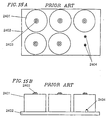
- Figures 15A and 15B are external views of a conventional dielectric notch filter.
- Figure 15A is a top view and Figure 15B is a side view.
- the dielectric notch filter includes cylindrical metal cavities 2401 , a base member 2402 , tuning members 2403 , and input/output terminals 2404 .
- the notch filter shown in Figure 15 has five resonators.
- a transmission line is formed in the base member 2402 and electromagnetically coupled with the respective dielectric resonators, so as to constitute the notch filter.
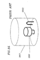
- Figure 16 shows the inside of a dielectric resonator used in the conventional dielectric notch filter shown in Figure 15 in a simplified manner.
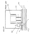
- FIG. 26 is a cross-sectional view showing an adjusting mechanism for adjusting the degree of electromagnetic coupling in the conventional dielectric resonator.
- the adjusting mechanism includes a supporting member 2 for supporting the dielectric block 2501 , a loop 4a of the coupling loop 2502 , a ground part 4b of the coupling loop 2502 , a handle 4c for rotating the whole coupling loop 2502 , and a pole 5 of the coupling loop 2502 .
- the pole 5 is composed of a center conductor 5a and an insulator 5b .
- the base member 2402 includes a transmission line 7 serving as an inner conductor and outer conductors 8 .
- the transmission line 7 is supported by a supporting member 9 which is an insulator.
- the dielectric block 2501 is formed integrally with and supported by the supporting member 2 using glass with a low melting point. The operation principle of the conventional dielectric resonator having the above-described construction will be described below.
- the conventional dielectric resonator has a resonance frequency corresponding to a resonant mode.
- the degree of electromagnetic coupling of the dielectric resonator is a critical parameter for determining the electric characteristic of the dielectric resonator.
- the degree of electromagnetic coupling is determined depending on the number of lines of magnetic force across the cross section of the coupling loop 2502 . That is, according to the conventional technique, the coupling loop 2502 is mechanically rotated by the handle 4c and hence the effective cross-sectional area is varied, so that the number of lines of magnetic force across the coupling loop 2502 is adjusted.
- the electric length of the coupling loop is precisely adjusted to be an odd-integer multiple of a quarter wavelength.
- the present invention thus concerns a dielectric resonator as defined in the appended claims.
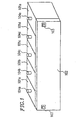
- Figure 1 is an external view of a dielectric notch filter in one example of the invention.
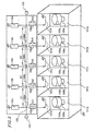
- Figure 2 is a view showing the internal construction of the dielectric notch filter in the example of the invention.
- Figure 3 is an equivalent circuit diagram of the dielectric notch filter in the example of the invention.
- Figure 4 is an equivalent circuit diagram in which a reactance element is connected to a series resonant circuit in parallel.
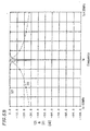
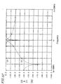
- Figures 5A through 5C are graphs of reflection and transmission characteristics with various reactance values of the reactance element in the circuit shown in Figure 4 .
- Figures 6A, 6B and 6C are equivalent circuit diagrams when a series resonant circuit is connected to the transmission line.
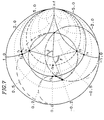
- Figure 7 is a diagram showing the frequency characteristics of the impedance of the dielectric resonator on the Smith Chart and showing frequencies for obtaining a resonance frequency and an External Q Qext.
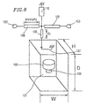
- Figure 8 is an explanatory diagram of an impedance converter.
- Figure 9 is an explanatory diagram of an impedance converter.
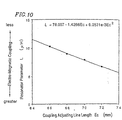
- Figure 10 shows the relationship between equivalent circuit parameter of the dielectric resonator and the coupling adjusting line length.
- Figure 11 is a view showing an exemplary construction of a coupling adjusting line 106 in the example of the invention.
- Figure 12 is a view showing another exemplary construction of a coupling adjusting line 106 in the example of the invention.
- Figure 13 is a view showing another exemplary construction of a coupling adjusting line 106 in the example of the invention.
- Figure 14 is a cross-sectional view for illustrating a method for holding the dielectric block in the example of the invention.
- Figure 15A is a top view of a conventional dielectric notch filter
- Figure 15B is a side view of the conventional dielectric notch filter shown in Figure 15A.
- Figure 16 is a view showing the inside construction of the conventional dielectric resonator.
- Figure 17 is a view of an electromagnetic coupling mechanism of a conventional dielectric resonator in detail.
- FIG. 1 is an external view of a dielectric notch filter in one example according to the invention.
- the dielectric notch filter of this example includes five dielectric resonators.
- Each dielectric resonator includes a box-type metal cavities 101a - 101e, tuning screws 104a - 104e, dielectric blocks 105a - 105e, coupling loops 107a - 107e , and supporting members 109a ⁇ 109e.
- the reference numeral 102 is a housing member of a transmission line for holding an inner conductor of a transmission line therein, and input/output connectors 103 are provided on the housing member 102 .
- the dielectric blocks 105a - 105e and the coupling loops 107a - 107e are provided in the metal cavities 101 - 101e, respectively.
- Figure 2 shows the inside construction of the notch filter of this example shown in Figure 1 by removing the cover portions of the metal cavities 101a - 101e.
- Figure 2 also shows the electric connection in the transmission-line housing member 102.
- the dielectric blocks 105a - 105e supported by the supporting members 109a - 109e and the coupling loops 107a - 107e are provided, respectively.
- Respective ends of coupling adjusting lines 106a - 106e having respective lengths of Ec1 - Ec5 are connected to a transmission line 108.
- transmission lines 108a - 108d having respective lengths of E1 - E4 are provided.
- the other ends of the coupling adjusting lines 106a - 106e are connected to the coupling loops 107a - 107e within the metal cavities 101a - 101e, respectively.
- reactance elements 110a - 110e are connected to the coupling adjusting lines 106a - 106e and the dielectric resonators, respectively, in parallel.
- the reactance elements 110a - 110e are connected for the purpose of matching the impedances of the respective dielectric resonators.
- the transmission line 108 and the dielectric blocks 105a - 105e are connected to each other via the electromagnetic coupling by the coupling loops 107a - 107e , respectively.
- FIG. 3 shows the equivalent circuit of the notch filter.
- Each of the above-described dielectric resonators is represented as a series resonant circuit shown in Figure 3 .
- the dielectric notch filter of the invention functions as a band rejection filter for removing signals having a specific frequency.
- desired notch filter characteristics can be obtained.
- One of the main features of the invention is the use of a method in which the lengths Ec1 - Ec5 of the coupling adjusting lines 106a - 106e and the values of the reactance elements 110a - 110e are changed by adopting the coupling adjusting lines 106a - 106e as a means for adjusting the degree of electromagnetic coupling of the dielectric resonator. How the equivalent circuit parameters can be adjusted by the length Ec1 - Ec5 of the coupling adjusting lines 106a - 106e and the reactance elements 110a - 110e will be described below with reference to the relevant figures and the experimental data.
- the reactance elements 110a - 110e are provided for matching the impedances of the respective dielectric resonators.
- An ideal resonator has no reactance component at a frequency which is sufficiently separated from the resonance point.
- Figure 4 shows a circuit in which a reactance element 401 is connected to a series resonant circuit in parallel.
- Figures 5A - 5C show the reflection characteristic (hereinafter referred to as S11) and the transmission characteristic (hereinafter referred to as . S21) when the reactance value of the reactance element 401 is changed in Figure 4 and the impedance of the whole circuit is changed from an inductive state to a capacitive state.
- Figure 5A shows the case where the dielectric resonator is inductive.
- Figure 5B shows the case where the dielectric resonator is neither inductive nor capacitive, i.e., the case where the impedance is matched.
- Figure 5C shows the dielectric resonator is capacitive.
- both S11 and S21 are asymmetric with respect to the resonance frequency, and the dielectric resonator does not operate as an ideal resonator. Accordingly, if the impedance of the dielectric resonator is inductive or capacitive ( Figure 5A or 5C ), a reactance element 110 is connected in parallel to the dielectric capacitor, thereby canceling the inductive state or the capacitive state of the dielectric resonator. As a result, the state in which the impedance is matched ( Figure 5B ) can be realized.
- the reactance element 110 is set to be capacitive for the inductive dielectric resonator, and the reactance element 110 is set to be inductive for the capacitive dielectric resonator.
- f 0 denotes the resonance frequency of the dielectric resonator
- f 1 and f 2 denote frequencies at which the absolute value of the reactance component of the dielectric resonator is equal to an external load value.
- the External Q Qext of the dielectric resonator can be obtained by Expression (1) below.
- Qext f 0 / (f 1 - f 2 )
- the value of (f 1 - f 2 ) is increased (i.e., the band is widened), and the value of Qext is decreased.
- Figure 8 shows a circuit of a dielectric resonator which is used in the experiment.
- the circuit corresponds to one of the five stages of the dielectric resonators in the above-described band rejection filter.
- the circuit is a 1-stage band rejection filter to which a transmission line 108 having a desired length and input/output connectors 103 are connected.
- a reactance element 110 is connected in parallel to the dielectric resonant at the point at which a coupling adjusting line 106 is connected to a transmission line 108 .
- Figure 9 shows an equivalent circuit of the dielectric resonator shown in Figure 8 .
- the length Ec of the employed coupling adjusting line 106 is selected to be 66, 68, 70, and 72 millimeters (mm).
- the employed cavity 101 has an inner size of 108 (wide) x 140 (depth) x 110 (height) mm.
- the side portion thereof is made of copper-plated iron, and the ceiling portion and the bottom portion are made of aluminum.
- the dielectric block 105 has an outer diameter of 62 mm, a height of 40 mm, and relative dielectric constant of 34.
- the dielectric block is supported by a 96% alumina supporting member 109 having an outer diameter of 35 mm, and a height of 30 mm.
- the coupling loop 107 has a cross section having an area of 650 mm 2 and is horizontally attached to the center of the side portion of the cavity 101 in the width (W) direction thereof.
- Figure 10 shows the experimental result of the relationship between the inductance value L of the equivalent circuit parameter of the dielectric resonator and the length Ec of the coupling adjusting line.
- the vertical axis indicates the value of L, and the horizontal axis indicates Ec.
- the vertical axis corresponds to the degree of electromagnetic . coupling of the dielectric resonator.
- the degree of electromagnetic coupling is increased, as the value of L is decreased.
- Figure 10 it has been found that, when the length of the transmission line is changed from 66 mm to 72 mm, the value of L is changed from 10.3 x 10 -6 (H) to 6.7 x 10 -6 (H).
- L 78.097 - 1.4266Ec + 6.0531 x 10 -3 Ec 2 (x 10 -6 (H))
- the coupling adjusting line 106 is always required, and the coupling adjusting line 106 is positively utilized for the impedance conversion (the adjustment of the degree of electromagnetic coupling) of the dielectric resonator, which is the main feature of the invention.
- the relationship between L and Ec shown in Expression (4) is only an example in the case where the cavity, the coupling loop, and the dielectric block employed have the above-defined sizes. It is appreciated that if a cavity, a coupling loop and a dielectric loop having other sizes and shapes are used, it is possible to change the circuit parameters of the dielectric resonator by means of the length of the coupling adjusting line.
- the lengths Ec1 - Ec5 of the coupling adjusting lines 106a - 106e can be adjusted by the following methods.
- a substrate on which a pattern such as shown in Figures 11 and 12 is printed can be used as the coupling adjusting line.
- the path through which the current flows is changed, and hence the electrical length is varied.
- Figure 12 a long pattern and a short pattern is connected in parallel. Therefore, in the state where the pattern is not shaved off, the current mainly flows through the short pattern. If the short pattern is cut off, the current starts to flow through the long pattern, so that the electrical length is varied.
- an alumina substrate, a polytetrafluoroethylene substrate, a glass epoxy substrate, or the like is used, and the substrate has, for example, a length of 30 - 50 mm and a breadth of 20 - 30 mm.
- a material of the pattern copper or the like is used, and the width of the pattern is, for example, 5 mm.
- the impedance matching elements 110a - 110e can be formed on the substrate. In such a case, the number of components can be decreased.
- the electrical length Ece of the transmission line can be changed. According to this method, the electrical length can be precisely adjusted without causing unwanted shavings.
- the connecting position of the reactance element is preferably connected at a position where the transmission line 108 and the coupling adjusting line 106 are connected.
- the reason is that, when viewed from the side on which the transmission line 108 is provided, the portion on the side on which the dielectric block is provided from the coupling adjusting line 106 , i.e., the portion on the side on which the dielectric block is provided from the connecting point of the transmission line 108 and the coupling adjusting line 106 is regarded as a dielectric resonator.
- the reactance element 110 is provided for matching the impedance of the dielectric resonator.
- the dielectric resonator does not operate as ideal resonator, because the dielectric resonator is not matched in view of the connecting point of the transmission line 108 and the coupling adjusting line 106. It is important to connect the transmission line 108 , the coupling adjusting line 106 and the reactance element 110 at "one point".
- the lengths of transmission lines between points at which the respective dielectric resonators are connected function as impedance inverters, and the lengths are critical parameters for designing the notch filter. Accordingly, by connecting the reactance element 110 at a point at which the transmission line 108 and the coupling adjusting line 106 are connected, a desired impedance inverter can be realized as an electrical length between the respective points at which the transmission line 108 , the coupling adjusting line 106 , and the reactance element 110 are connected. As a result, the notch filter characteristics which are determined during the designing can be obtained.
- the reactance element 110 for example, an air-core coil, a capacitor having parallel plate electrodes, a transmission line stub, or the like is used.
- the air-core coil is used as the reactance element 110 , the impedance characteristic of the dielectric resonator can be easily adjusted by deforming the air-core coil.
- the total length of the coupling adjusting line and the coupling loop can be set to be larger than a quarter wavelength or an odd-integer multiple of a quarter wavelength by one-eighth of the wavelength or less.
- an inductor is connected in parallel to the open end of the coupling loop, and hence the impedance of the dielectric resonator can be matched.
- the method is very easily performed.
- Figure 14 shows a method for attaching the dielectric block 105 to the metal cavity 101 , and shows the cross section of the cylindrical dielectric block 105 along the center axis thereof.
- the dielectric block 105 is supported by a cylindrical supporting member 109 which is engaged with a recessed portion 1405 of the dielectric block 105 .
- the dielectric block 105 and the supporting member 109 are fixed to each other by a bolt 1401 , a nut 1402 , and a washer 1403 which are made of a resin.
- a bolt pressing plate 1404 has a center hole through which the bolt 1401 is attached, and the bolt pressing plate 1404 is fixed to the metal cavity 101 by means of screws 1406 .
- the bolt 1401 passes through the bolt pressing plate 1404 , the supporting member 109 , the dielectric block 105 , the washer 1403 , and the nut 1402 , in this order, so as to make them as an integral unit.
- the washer 1403 has a protrusion which is fitted in the through hole of the dielectric block 105 for positioning the dielectric block 105.
- the nut 1402 may have a protrusion which ensures that the dielectric block 105 can be located in position.
- the metal cavity 101 has a hole for accommodating the head of the bolt 1401 and holes through which the screws 1406 for fixing the bolt pressing plate 1404.
- the bolt 1401 passes through the central portion of the dielectric block 105 with a lower magnetic flux density in the electromagnetic field generated in the metal cavity 101 for fixing the dielectric block 105.
- a material of the bolt 1401 , the nut 1402 , and the washer 1403 a material with a lower dielectric constant is preferable for increasing the value of Q.
- the supporting member 109 is formed of a material having a relatively small dielectric constant, the magnetic flux density in the vicinity of the bottom face of the metal cavity 101 can be lowered, so that it is possible to realize a dielectric resonator having a higher value of Q.
- a material having a dielectric constant which is one-third of the dielectric constant (30 to 45) of the dielectric block 105 such as alumina, magnesia, forsterite (the dielectric constant thereof is about 10), or the like can be used.
- the metal cavity 101 has a hole for accommodating the head of the bolt 1401 , and the thickness of the metal cavity 101 around the hole is set to be larger than the thickness of the head of the bolt 1401 .
- the thickness of the metal cavity 101 around the hole is set to be larger than the thickness of the head of the bolt 1401 .
- the recessed portion 1405 is formed on the lower face of the dielectric block 105 , and the protrusion is provided on the center portion of the washer 1403 , so that the positioning of the dielectric block 105 with respect to the metal cavity 101 can be easily and precisely performed. Moreover, it is possible to prevent the resonance frequency and the degree of coupling to be varied.
- the bolt When an electromagnetic resonant mode of the TE mode is used, the bolt is allowed to pass through the through hole which is parallel with the propagation axis direction and is fixed by the washer and the nut, whereby it is possible to fix the dielectric block to the cavity. As a result, it is possible to minimize the deterioration of the value of Q caused by the bolt, the washer, and the nut.
Landscapes
- Physics & Mathematics (AREA)
- Electromagnetism (AREA)
- Control Of Motors That Do Not Use Commutators (AREA)
Claims (8)
- Résonateur diélectrique comprenant :une cavité (101) comportant une paroi de délimitation,un bloc diélectrique (105) fixé dans la cavité (101) et,un dispositif de couplage (106) couplé par un champ électromagnétique produit dans la cavité,dans lequel un trou traversant est formé dans le bloc diélectrique (105), un axe de fixation (1401) formé d'un matériau diélectrique peut passer au travers du trou traversant, et une première extrémité de l'axe de fixation (1401) est fixée à la paroi de la cavité par un élément de pression (1404, 1406), le résonateur comprenant en outreun élément de support (109) comportant un trou traversant au travers duquel l'axe de fixation (1401) peut passer, le bloc diélectrique étant supporté par l'élément de support (109),
caractérisé en ce quele bloc diélectrique (105) comporte une partie en retrait (1405) dans son plan inférieur et ledit élément de support (109) est en prise avec ladite partie en retrait (1405), et en ce quel'élément de support (109) est formé d'un matériau présentant une constante diélectrique relativement faible par comparaison à celle du bloc diélectrique (105) de manière à abaisser la densité du flux magnétique à proximité de la face inférieure de la cavité (101), en obtenant ainsi un résonateur diélectrique présentant une valeur plus élevée de facteur de qualité Q. - Résonateur diélectrique selon la revendication 1, dans lequel le bloc diélectrique (105) résonne dans un mode TE, et le trou traversant est prévu parallèlement à la direction de l'axe d'un trajet de propagation de mode.
- Résonateur diélectrique selon la revendication 1, dans lequel l'axe de fixation (1401) est fileté et l'élément de pression est un écrou de résine (1402).
- Résonateur diélectrique selon la revendication 3, dans lequel l'écrou de résine (1402) est muni d'une protubérance qui s'adapte dans le trou traversant.
- Résonateur diélectrique selon la revendication 3, dans lequel une rondelle de résine (1403) présentant une protubérance qui s'adapte dans le trou traversant est prise en sandwich entre l'écrou de résine (1402) et le bloc diélectrique (105).
- Résonateur diélectrique selon la revendication 1, dans lequel le diamètre du trou traversant est plus grand que le diamètre de l'axe de fixation (1401) et un intervalle est prévu entre le bloc diélectrique (105) et l'axe de fixation (1401).
- Résonateur diélectrique comprenant :un boulon (1401) formé d'un matériau diélectrique,une plaque d'appui de boulon (1404) comportant un trou traversant,un élément de support (109) comportant un trou traversant,un bloc diélectrique (105) comportant un trou traversant, et une cavité (101) comportant une paroi de délimitation,dans lequel le boulon (1401) peut passer au travers des trous traversants de la plaque d'appui de boulon (1404), de l'élément de support (109), et du bloc diélectrique (105) dans cet ordre, et est fixé avec un écrou, en constituant ainsi une unité de résonateur, l'unité de résonateur étant fixée à la paroi de la cavité,
caractérisé en ce quele bloc diélectrique (105) comporte une partie en retrait (1405) dans son plan inférieur et ledit élément de support (109) est en prise avec ladite partie en retrait (1405), et en ce quel'élément de support (109) est formé d'un matériau présentant une constante diélectrique relativement faible par comparaison à celle du bloc diélectrique (105) de manière à abaisser la densité du flux magnétique à proximité de la face inférieure de la cavité (101), en obtenant ainsi un résonateur diélectrique présentant une valeur plus élevée de facteur de qualité Q. - Résonateur diélectrique selon la revendication 7, dans lequel une partie de la paroi de la cavité à laquelle l'unité de résonateur est fixée présente une épaisseur plus grande qu'une épaisseur d'une partie de tête du boulon (1401), et une ouverture est ménagée afin de permettre à la partie de tête du boulon de passer, l'ouverture étant refermée par la plaque d'appui de boulon (1404).
Applications Claiming Priority (7)
| Application Number | Priority Date | Filing Date | Title |
|---|---|---|---|
| JP25417093 | 1993-10-12 | ||
| JP254170/93 | 1993-10-12 | ||
| JP25417093 | 1993-10-12 | ||
| JP27411293 | 1993-11-02 | ||
| JP274112/93 | 1993-11-02 | ||
| JP27411293 | 1993-11-02 | ||
| EP94115968A EP0647975B1 (fr) | 1993-10-12 | 1994-10-10 | Résonateur diélectrique, filtre coupe-bande diélectrique et filtre diélectrique |
Related Parent Applications (1)
| Application Number | Title | Priority Date | Filing Date |
|---|---|---|---|
| EP94115968A Division EP0647975B1 (fr) | 1993-10-12 | 1994-10-10 | Résonateur diélectrique, filtre coupe-bande diélectrique et filtre diélectrique |
Publications (2)
| Publication Number | Publication Date |
|---|---|
| EP0877434A1 EP0877434A1 (fr) | 1998-11-11 |
| EP0877434B1 true EP0877434B1 (fr) | 2001-06-13 |
Family
ID=26541563
Family Applications (4)
| Application Number | Title | Priority Date | Filing Date |
|---|---|---|---|
| EP98113083A Expired - Lifetime EP0877434B1 (fr) | 1993-10-12 | 1994-10-10 | Résonateur diélectrique |
| EP98113085A Expired - Lifetime EP0877435B1 (fr) | 1993-10-12 | 1994-10-10 | Résonator diélectrique, filtre coupe-bande diélectrique et filtre diélectrique |
| EP94115968A Expired - Lifetime EP0647975B1 (fr) | 1993-10-12 | 1994-10-10 | Résonateur diélectrique, filtre coupe-bande diélectrique et filtre diélectrique |
| EP98113084A Expired - Lifetime EP0880192B1 (fr) | 1993-10-12 | 1994-10-10 | Résonateur diélectrique et filtre diélectrique |
Family Applications After (3)
| Application Number | Title | Priority Date | Filing Date |
|---|---|---|---|
| EP98113085A Expired - Lifetime EP0877435B1 (fr) | 1993-10-12 | 1994-10-10 | Résonator diélectrique, filtre coupe-bande diélectrique et filtre diélectrique |
| EP94115968A Expired - Lifetime EP0647975B1 (fr) | 1993-10-12 | 1994-10-10 | Résonateur diélectrique, filtre coupe-bande diélectrique et filtre diélectrique |
| EP98113084A Expired - Lifetime EP0880192B1 (fr) | 1993-10-12 | 1994-10-10 | Résonateur diélectrique et filtre diélectrique |
Country Status (3)
| Country | Link |
|---|---|
| US (4) | US5714919A (fr) |
| EP (4) | EP0877434B1 (fr) |
| DE (4) | DE69427493T2 (fr) |
Families Citing this family (64)
| Publication number | Priority date | Publication date | Assignee | Title |
|---|---|---|---|---|
| US6026311A (en) * | 1993-05-28 | 2000-02-15 | Superconductor Technologies, Inc. | High temperature superconducting structures and methods for high Q, reduced intermodulation resonators and filters |
| US7231238B2 (en) * | 1989-01-13 | 2007-06-12 | Superconductor Technologies, Inc. | High temperature spiral snake superconducting resonator having wider runs with higher current density |
| US5843871A (en) * | 1995-11-13 | 1998-12-01 | Illinois Superconductor Corporation | Electromagnetic filter having a transmission line disposed in a cover of the filter housing |
| US5949309A (en) * | 1997-03-17 | 1999-09-07 | Communication Microwave Corporation | Dielectric resonator filter configured to filter radio frequency signals in a transmit system |
| US7301748B2 (en) | 1997-04-08 | 2007-11-27 | Anthony Anthony A | Universal energy conditioning interposer with circuit architecture |
| US7336468B2 (en) | 1997-04-08 | 2008-02-26 | X2Y Attenuators, Llc | Arrangement for energy conditioning |
| US6894884B2 (en) | 1997-04-08 | 2005-05-17 | Xzy Attenuators, Llc | Offset pathway arrangements for energy conditioning |
| US6018448A (en) | 1997-04-08 | 2000-01-25 | X2Y Attenuators, L.L.C. | Paired multi-layered dielectric independent passive component architecture resulting in differential and common mode filtering with surge protection in one integrated package |
| US20030161086A1 (en) | 2000-07-18 | 2003-08-28 | X2Y Attenuators, Llc | Paired multi-layered dielectric independent passive component architecture resulting in differential and common mode filtering with surge protection in one integrated package |
| US7042703B2 (en) | 2000-03-22 | 2006-05-09 | X2Y Attenuators, Llc | Energy conditioning structure |
| US7110235B2 (en) * | 1997-04-08 | 2006-09-19 | Xzy Altenuators, Llc | Arrangement for energy conditioning |
| US9054094B2 (en) | 1997-04-08 | 2015-06-09 | X2Y Attenuators, Llc | Energy conditioning circuit arrangement for integrated circuit |
| US6606011B2 (en) | 1998-04-07 | 2003-08-12 | X2Y Attenuators, Llc | Energy conditioning circuit assembly |
| US7321485B2 (en) | 1997-04-08 | 2008-01-22 | X2Y Attenuators, Llc | Arrangement for energy conditioning |
| US7274549B2 (en) | 2000-12-15 | 2007-09-25 | X2Y Attenuators, Llc | Energy pathway arrangements for energy conditioning |
| WO1999052210A1 (fr) | 1998-04-07 | 1999-10-14 | X2Y Attenuators, L.L.C. | Support de composants |
| US7106570B2 (en) | 1997-04-08 | 2006-09-12 | Xzy Altenuators, Llc | Pathway arrangement |
| US7110227B2 (en) | 1997-04-08 | 2006-09-19 | X2Y Attenuators, Llc | Universial energy conditioning interposer with circuit architecture |
| US6954346B2 (en) | 1997-04-08 | 2005-10-11 | Xzy Attenuators, Llc | Filter assembly |
| US6603646B2 (en) | 1997-04-08 | 2003-08-05 | X2Y Attenuators, Llc | Multi-functional energy conditioner |
| US6650525B2 (en) | 1997-04-08 | 2003-11-18 | X2Y Attenuators, Llc | Component carrier |
| US7336467B2 (en) | 2000-10-17 | 2008-02-26 | X2Y Attenuators, Llc | Energy pathway arrangement |
| JP3506013B2 (ja) | 1997-09-04 | 2004-03-15 | 株式会社村田製作所 | 多重モード誘電体共振器装置、誘電体フィルタ、複合誘電体フィルタ、合成器、分配器および通信装置 |
| JP3503482B2 (ja) | 1997-09-04 | 2004-03-08 | 株式会社村田製作所 | 多重モード誘電体共振器装置、誘電体フィルタ、複合誘電体フィルタ、合成器、分配器、および通信装置 |
| US7427816B2 (en) | 1998-04-07 | 2008-09-23 | X2Y Attenuators, Llc | Component carrier |
| JPH11312910A (ja) * | 1998-04-28 | 1999-11-09 | Murata Mfg Co Ltd | 誘電体共振器、誘電体フィルタ、誘電体デュプレクサおよび通信機装置ならびに誘電体共振器の製造方法 |
| US6222428B1 (en) * | 1999-06-15 | 2001-04-24 | Allgon Ab | Tuning assembly for a dielectrical resonator in a cavity |
| US6707353B1 (en) * | 1999-11-02 | 2004-03-16 | Matsushita Electric Industrial Co., Ltd. | Dielectric filter |
| EP1230710A1 (fr) * | 1999-11-12 | 2002-08-14 | Trilithic, Inc. | Ameliorations de filtres a cavite |
| US7113383B2 (en) | 2000-04-28 | 2006-09-26 | X2Y Attenuators, Llc | Predetermined symmetrically balanced amalgam with complementary paired portions comprising shielding electrodes and shielded electrodes and other predetermined element portions for symmetrically balanced and complementary energy portion conditioning |
| CN1571214A (zh) * | 2000-05-23 | 2005-01-26 | 松下电器产业株式会社 | 电介质谐振滤波器及其非需要模式抑制方法 |
| SE516862C2 (sv) * | 2000-07-14 | 2002-03-12 | Allgon Ab | Avstämningsskruvanordning samt metod och resonator |
| EP1312148A4 (fr) | 2000-08-15 | 2009-06-03 | X2Y Attenuators Llc | Systeme d'electrodes pour conditionnement d'energie en circuit |
| US20040036557A1 (en) * | 2000-08-29 | 2004-02-26 | Takehiko Yamakawa | Dielectric filter |
| US7193831B2 (en) | 2000-10-17 | 2007-03-20 | X2Y Attenuators, Llc | Energy pathway arrangement |
| KR100536511B1 (ko) | 2000-10-17 | 2005-12-14 | 엑스2와이 어테뉴에이터스, 엘.엘.씨 | 공통 기준 노드를 갖는 단일 또는 다수의 회로들을 위한 차폐 아말감 및 차폐된 에너지 경로들 및 다른 엘리먼트들 |
| SE517746C2 (sv) * | 2000-10-20 | 2002-07-09 | Ericsson Telefon Ab L M | Lageranordning, Kavitetsfilter samt förfarande för montering därav |
| TW494241B (en) * | 2000-12-14 | 2002-07-11 | Ind Tech Res Inst | Circular type coupled microwave cavity |
| US6919782B2 (en) * | 2001-04-04 | 2005-07-19 | Adc Telecommunications, Inc. | Filter structure including circuit board |
| US6975181B2 (en) * | 2001-05-31 | 2005-12-13 | Sei-Joo Jang | Dielectric resonator loaded metal cavity filter |
| US6633208B2 (en) * | 2001-06-19 | 2003-10-14 | Superconductor Technologies, Inc. | Filter with improved intermodulation distortion characteristics and methods of making the improved filter |
| US6642814B2 (en) | 2001-12-17 | 2003-11-04 | Alcatel, Radio Frequency Systems, Inc. | System for cross coupling resonators |
| US6987916B2 (en) | 2001-12-18 | 2006-01-17 | Alcatel | Fiber optic central tube cable with bundled support member |
| US7071797B2 (en) * | 2002-02-19 | 2006-07-04 | Conductus, Inc. | Method and apparatus for minimizing intermodulation with an asymmetric resonator |
| EP1372211A3 (fr) * | 2002-06-12 | 2004-01-07 | Matsushita Electric Industrial Co., Ltd. | Filtre diélectrique, appareil de communication et procédé de contrôle de la fréquence de résonance |
| US7180718B2 (en) | 2003-01-31 | 2007-02-20 | X2Y Attenuators, Llc | Shielded energy conditioner |
| WO2005002018A2 (fr) | 2003-05-29 | 2005-01-06 | X2Y Attenuators, Llc | Connecteur se rapportant a des structures comprenant un conditionneur d'energie |
| KR100565218B1 (ko) * | 2003-09-08 | 2006-03-30 | 엘지전자 주식회사 | 무전극 조명기기의 공진기구조 |
| KR20060120683A (ko) | 2003-12-22 | 2006-11-27 | 엑스2와이 어테뉴에이터스, 엘.엘.씨 | 내부적으로 차폐된 에너지 컨디셔너 |
| WO2006093831A2 (fr) | 2005-03-01 | 2006-09-08 | X2Y Attenuators, Llc | Conditionneur d'energie avec electrodes traversantes reliees |
| JP2008537843A (ja) | 2005-03-01 | 2008-09-25 | エックストゥーワイ アテニュエイターズ,エルエルシー | 内部で重なり合った調整器 |
| WO2006099297A2 (fr) | 2005-03-14 | 2006-09-21 | X2Y Attenuators, Llc | Conditionneur a conducteurs coplanaires |
| EP1991996A1 (fr) | 2006-03-07 | 2008-11-19 | X2Y Attenuators, L.L.C. | Structures de conditionneur d'énergie |
| CN101485040B (zh) * | 2006-07-13 | 2014-05-07 | 艾利森电话股份有限公司 | 波导滤波器的微调 |
| ES2781828T3 (es) | 2008-11-19 | 2020-09-08 | Boehringer Ingelheim Animal Health Usa Inc | Composiciones que comprenden un aril pirazol y/o una formamidina, procedimientos y usos de las mismas |
| EP2355235A1 (fr) * | 2010-01-29 | 2011-08-10 | Astrium Limited | Appareil de filtrage d'un signal d'entrée |
| WO2012025946A1 (fr) * | 2010-08-25 | 2012-03-01 | Commscope Italy S.R.L. | Filtre passe-bande accordable |
| DE102012106174A1 (de) * | 2012-07-10 | 2014-01-16 | Endress + Hauser Gmbh + Co. Kg | Mit einer Störwellen aussendenden Hochfrequenzbaugruppe ausgestattete Leiterplatte |
| KR101345807B1 (ko) | 2013-05-29 | 2013-12-27 | 주식회사 케오솔 | 유전체 필터 모듈을 이용한 맞춤형 전류 흐름 개선장치 |
| CN107112615B (zh) * | 2014-12-31 | 2019-11-26 | 深圳市大富科技股份有限公司 | 腔体滤波器、双工器、信号收发装置、射频拉远设备和塔顶放大器 |
| CN105322258B (zh) * | 2015-11-17 | 2019-01-22 | 强胜精密机械(苏州)有限公司 | 一种腔体滤波器盖板 |
| CN111326842A (zh) * | 2018-12-14 | 2020-06-23 | 中兴通讯股份有限公司 | 一种谐振器及滤波器 |
| CN111446524B (zh) * | 2019-01-17 | 2022-04-08 | 罗森伯格技术有限公司 | 一种单层交叉耦合滤波器 |
| CN110416671B (zh) * | 2019-06-12 | 2021-11-02 | 广东通宇通讯股份有限公司 | 谐振器、腔体滤波器及其调试方法 |
Family Cites Families (28)
| Publication number | Priority date | Publication date | Assignee | Title |
|---|---|---|---|---|
| DE1275169B (de) * | 1962-08-30 | 1968-08-14 | Siemens Ag | Anordnung zur Ankopplung wenigstens eines Resonanzkreises fuer sehr kurze elektromagnetische Wellen an wenigstens einen Anschlusshohlleiter |
| GB1281564A (en) * | 1969-03-03 | 1972-07-12 | Marconi Co Ltd | Improvements in or relating to waveguide filters |
| US3618994A (en) * | 1969-05-14 | 1971-11-09 | Loopco Industries | Arbor nut |
| DE2538614C3 (de) * | 1974-09-06 | 1979-08-02 | Murata Manufacturing Co., Ltd., Nagaokakyo, Kyoto (Japan) | Dielektrischer Resonator |
| DE2544498C3 (de) * | 1975-10-04 | 1981-05-21 | Spieth-Maschinenelemente Gmbh & Co Kg, 7300 Esslingen | Gewindering |
| US4121181A (en) * | 1976-06-14 | 1978-10-17 | Murata Manufacturing Co., Ltd. | Electrical branching filter |
| SU624325A1 (ru) * | 1976-12-03 | 1978-09-15 | Предприятие П/Я Х-5734 | Ячейка заграждающего фильтра |
| US4124830A (en) * | 1977-09-27 | 1978-11-07 | Bell Telephone Laboratories, Incorporated | Waveguide filter employing dielectric resonators |
| US4477788A (en) * | 1983-02-03 | 1984-10-16 | M/A Com, Inc. | Dielectric resonator tuner and mechanical mounting system |
| US4728913A (en) * | 1985-01-18 | 1988-03-01 | Murata Manufacturing Co., Ltd. | Dielectric resonator |
| EP0235123B1 (fr) * | 1985-07-08 | 1991-11-21 | Space Systems / Loral, Inc. | Filtre a bande etroite comportant un resonateur dielectrique |
| JPS6230404A (ja) * | 1985-08-01 | 1987-02-09 | Murata Mfg Co Ltd | ストリツプラインフイルタ |
| JPS6239902A (ja) * | 1985-08-14 | 1987-02-20 | Murata Mfg Co Ltd | 帯域阻止形フイルタ回路 |
| US4896125A (en) * | 1988-12-14 | 1990-01-23 | Alcatel N.A., Inc. | Dielectric notch resonator |
| US4862122A (en) * | 1988-12-14 | 1989-08-29 | Alcatel Na, Inc | Dielectric notch filter |
| FR2649538B1 (fr) * | 1989-07-10 | 1991-12-13 | Alcatel Transmission | Boitier hyperfrequence a vis de reglage |
| US5191304A (en) * | 1990-03-02 | 1993-03-02 | Orion Industries, Inc. | Bandstop filter having symmetrically altered or compensated quarter wavelength transmission line sections |
| US5065119A (en) * | 1990-03-02 | 1991-11-12 | Orion Industries, Inc. | Narrow-band, bandstop filter |
| US5051714A (en) * | 1990-03-08 | 1991-09-24 | Alcatel Na, Inc. | Modular resonant cavity, modular dielectric notch resonator and modular dielectric notch filter |
| JPH0425303U (fr) * | 1990-06-22 | 1992-02-28 | ||
| CA2048404C (fr) * | 1991-08-02 | 1993-04-13 | Raafat R. Mansour | Filtres bimodes avec resonateurs dielectriques a ouvertures |
| JP2699704B2 (ja) * | 1991-08-19 | 1998-01-19 | 株式会社村田製作所 | 帯域阻止型フィルタ |
| JPH0598305A (ja) * | 1991-10-08 | 1993-04-20 | Sumitomo Metal Mining Co Ltd | 酸化パラジウム被覆パラジウム粉末の製造方法 |
| JPH0661713A (ja) * | 1992-08-11 | 1994-03-04 | Murata Mfg Co Ltd | 誘電体共振器 |
| US5347246A (en) * | 1992-10-29 | 1994-09-13 | Gte Control Devices Incorporated | Mounting assembly for dielectric resonator device |
| US5373270A (en) * | 1993-12-06 | 1994-12-13 | Radio Frequency Systems, Inc. | Multi-cavity dielectric filter |
| US5612655A (en) * | 1995-07-06 | 1997-03-18 | Allen Telecom Group, Inc. | Filter assembly comprising a plastic resonator support and resonator tuning assembly |
| US6011446A (en) * | 1998-05-21 | 2000-01-04 | Delphi Components, Inc. | RF/microwave oscillator having frequency-adjustable DC bias circuit |
-
1994
- 1994-10-07 US US08/320,046 patent/US5714919A/en not_active Expired - Lifetime
- 1994-10-10 EP EP98113083A patent/EP0877434B1/fr not_active Expired - Lifetime
- 1994-10-10 EP EP98113085A patent/EP0877435B1/fr not_active Expired - Lifetime
- 1994-10-10 EP EP94115968A patent/EP0647975B1/fr not_active Expired - Lifetime
- 1994-10-10 DE DE69427493T patent/DE69427493T2/de not_active Expired - Lifetime
- 1994-10-10 EP EP98113084A patent/EP0880192B1/fr not_active Expired - Lifetime
- 1994-10-10 DE DE69424618T patent/DE69424618T2/de not_active Expired - Lifetime
- 1994-10-10 DE DE69431412T patent/DE69431412T2/de not_active Expired - Lifetime
- 1994-10-10 DE DE69427780T patent/DE69427780T2/de not_active Expired - Lifetime
-
1997
- 1997-07-10 US US08/891,272 patent/US6107900A/en not_active Expired - Lifetime
-
2000
- 2000-03-15 US US09/526,495 patent/US6222429B1/en not_active Expired - Lifetime
-
2001
- 2001-03-01 US US09/798,804 patent/US6414572B2/en not_active Expired - Lifetime
Also Published As
| Publication number | Publication date |
|---|---|
| EP0877434A1 (fr) | 1998-11-11 |
| DE69427493D1 (de) | 2001-07-19 |
| US20010011937A1 (en) | 2001-08-09 |
| EP0877435B1 (fr) | 2002-09-18 |
| EP0647975B1 (fr) | 2000-05-24 |
| DE69427780D1 (de) | 2001-08-23 |
| EP0647975A3 (fr) | 1995-06-28 |
| DE69431412D1 (de) | 2002-10-24 |
| DE69424618T2 (de) | 2001-02-08 |
| DE69427493T2 (de) | 2002-04-18 |
| DE69427780T2 (de) | 2002-05-23 |
| DE69431412T2 (de) | 2003-05-28 |
| EP0880192B1 (fr) | 2001-07-18 |
| EP0647975A2 (fr) | 1995-04-12 |
| US6222429B1 (en) | 2001-04-24 |
| US6107900A (en) | 2000-08-22 |
| EP0880192A1 (fr) | 1998-11-25 |
| US6414572B2 (en) | 2002-07-02 |
| EP0877435A1 (fr) | 1998-11-11 |
| US5714919A (en) | 1998-02-03 |
| DE69424618D1 (de) | 2000-06-29 |
Similar Documents
| Publication | Publication Date | Title |
|---|---|---|
| EP0877434B1 (fr) | Résonateur diélectrique | |
| KR102503237B1 (ko) | 무선 주파수 필터 | |
| EP0068504B1 (fr) | Filtre en forme de peigne | |
| WO2001013460A1 (fr) | Filtre a ondes ultracourtes | |
| JPH07263924A (ja) | 誘電体共振器 | |
| CA2262357C (fr) | Appareil dielectrique ayant une ligne de raccord si-jointe | |
| EP1034576A1 (fr) | Resonateur coaxial multisurface couple | |
| US6175286B1 (en) | Dielectric resonator and dielectric filter using the same | |
| EP1079457B1 (fr) | Dispositif à résonance diélectrique, filtre diélectrique, dispositif filtre diélectrique composé, duplexeur diélectrique et appareil de communication | |
| US4673894A (en) | Oscillator coupled through cylindrical cavity for generating low noise microwaves | |
| EP0743696B1 (fr) | Filtre diélectrique et procédé de fabrication | |
| JPH05206730A (ja) | 電圧制御発振器およびその発振周波数の調整方法 | |
| JPH07202528A (ja) | 誘電体同軸共振器および誘電体共振器フィルタ | |
| JP3606274B2 (ja) | 誘電体共振器、誘電体フィルタ | |
| EP1043798B1 (fr) | Filtre à résonateur diélectrique | |
| JP3570417B2 (ja) | 誘電体ノッチフィルタ | |
| JP3376716B2 (ja) | 誘電体共振器、誘電体ノッチフィルタおよび誘電体フィルタ | |
| KR0164092B1 (ko) | 소형화한 유전체 공진기 필터 | |
| KR200330762Y1 (ko) | 불효파 특성 개선을 위한 유전체 캐비티 여파기 | |
| JPH10107502A (ja) | 同軸形誘電体フィルタ | |
| JP2003124717A (ja) | 誘電体共振器 | |
| JP2003273605A (ja) | 導波管型フィルタ | |
| JPH11330817A (ja) | 誘電体共振器装置、誘電体フィルタ、発振器および電子機器 | |
| JP2003124704A (ja) | 誘電体フィルタ | |
| JPS60145702A (ja) | 誘電体ろ波器 |
Legal Events
| Date | Code | Title | Description |
|---|---|---|---|
| PUAI | Public reference made under article 153(3) epc to a published international application that has entered the european phase |
Free format text: ORIGINAL CODE: 0009012 |
|
| 17P | Request for examination filed |
Effective date: 19980731 |
|
| AC | Divisional application: reference to earlier application |
Ref document number: 647975 Country of ref document: EP |
|
| AK | Designated contracting states |
Kind code of ref document: A1 Designated state(s): DE FR GB SE |
|
| 17Q | First examination report despatched |
Effective date: 19990806 |
|
| GRAG | Despatch of communication of intention to grant |
Free format text: ORIGINAL CODE: EPIDOS AGRA |
|
| RTI1 | Title (correction) |
Free format text: DIELECTRIC RESONATOR |
|
| RTI1 | Title (correction) |
Free format text: DIELECTRIC RESONATOR |
|
| GRAG | Despatch of communication of intention to grant |
Free format text: ORIGINAL CODE: EPIDOS AGRA |
|
| GRAH | Despatch of communication of intention to grant a patent |
Free format text: ORIGINAL CODE: EPIDOS IGRA |
|
| GRAH | Despatch of communication of intention to grant a patent |
Free format text: ORIGINAL CODE: EPIDOS IGRA |
|
| GRAA | (expected) grant |
Free format text: ORIGINAL CODE: 0009210 |
|
| AC | Divisional application: reference to earlier application |
Ref document number: 647975 Country of ref document: EP |
|
| AK | Designated contracting states |
Kind code of ref document: B1 Designated state(s): DE FR GB SE |
|
| REF | Corresponds to: |
Ref document number: 69427493 Country of ref document: DE Date of ref document: 20010719 |
|
| ET | Fr: translation filed | ||
| REG | Reference to a national code |
Ref country code: GB Ref legal event code: IF02 |
|
| PLBE | No opposition filed within time limit |
Free format text: ORIGINAL CODE: 0009261 |
|
| STAA | Information on the status of an ep patent application or granted ep patent |
Free format text: STATUS: NO OPPOSITION FILED WITHIN TIME LIMIT |
|
| 26N | No opposition filed | ||
| PGFP | Annual fee paid to national office [announced via postgrant information from national office to epo] |
Ref country code: FR Payment date: 20131009 Year of fee payment: 20 Ref country code: DE Payment date: 20131002 Year of fee payment: 20 Ref country code: SE Payment date: 20131011 Year of fee payment: 20 Ref country code: GB Payment date: 20131009 Year of fee payment: 20 |
|
| REG | Reference to a national code |
Ref country code: DE Ref legal event code: R071 Ref document number: 69427493 Country of ref document: DE |
|
| REG | Reference to a national code |
Ref country code: GB Ref legal event code: PE20 Expiry date: 20141009 |
|
| REG | Reference to a national code |
Ref country code: SE Ref legal event code: EUG |
|
| PG25 | Lapsed in a contracting state [announced via postgrant information from national office to epo] |
Ref country code: GB Free format text: LAPSE BECAUSE OF EXPIRATION OF PROTECTION Effective date: 20141009 |