EP0878729A2 - Polarisationsunabhängiger optischer Phasenmodulator - Google Patents
Polarisationsunabhängiger optischer Phasenmodulator Download PDFInfo
- Publication number
- EP0878729A2 EP0878729A2 EP98303574A EP98303574A EP0878729A2 EP 0878729 A2 EP0878729 A2 EP 0878729A2 EP 98303574 A EP98303574 A EP 98303574A EP 98303574 A EP98303574 A EP 98303574A EP 0878729 A2 EP0878729 A2 EP 0878729A2
- Authority
- EP
- European Patent Office
- Prior art keywords
- modulator
- liquid crystal
- layer
- disposed
- alignment
- Prior art date
- Legal status (The legal status is an assumption and is not a legal conclusion. Google has not performed a legal analysis and makes no representation as to the accuracy of the status listed.)
- Granted
Links
Images


Classifications
-
- G—PHYSICS
- G02—OPTICS
- G02F—OPTICAL DEVICES OR ARRANGEMENTS FOR THE CONTROL OF LIGHT BY MODIFICATION OF THE OPTICAL PROPERTIES OF THE MEDIA OF THE ELEMENTS INVOLVED THEREIN; NON-LINEAR OPTICS; FREQUENCY-CHANGING OF LIGHT; OPTICAL LOGIC ELEMENTS; OPTICAL ANALOGUE/DIGITAL CONVERTERS
- G02F1/00—Devices or arrangements for the control of the intensity, colour, phase, polarisation or direction of light arriving from an independent light source, e.g. switching, gating or modulating; Non-linear optics
- G02F1/29—Devices or arrangements for the control of the intensity, colour, phase, polarisation or direction of light arriving from an independent light source, e.g. switching, gating or modulating; Non-linear optics for the control of the position or the direction of light beams, i.e. deflection
- G02F1/292—Devices or arrangements for the control of the intensity, colour, phase, polarisation or direction of light arriving from an independent light source, e.g. switching, gating or modulating; Non-linear optics for the control of the position or the direction of light beams, i.e. deflection by controlled diffraction or phased-array beam steering
-
- G—PHYSICS
- G02—OPTICS
- G02F—OPTICAL DEVICES OR ARRANGEMENTS FOR THE CONTROL OF LIGHT BY MODIFICATION OF THE OPTICAL PROPERTIES OF THE MEDIA OF THE ELEMENTS INVOLVED THEREIN; NON-LINEAR OPTICS; FREQUENCY-CHANGING OF LIGHT; OPTICAL LOGIC ELEMENTS; OPTICAL ANALOGUE/DIGITAL CONVERTERS
- G02F1/00—Devices or arrangements for the control of the intensity, colour, phase, polarisation or direction of light arriving from an independent light source, e.g. switching, gating or modulating; Non-linear optics
- G02F1/01—Devices or arrangements for the control of the intensity, colour, phase, polarisation or direction of light arriving from an independent light source, e.g. switching, gating or modulating; Non-linear optics for the control of the intensity, phase, polarisation or colour
- G02F1/13—Devices or arrangements for the control of the intensity, colour, phase, polarisation or direction of light arriving from an independent light source, e.g. switching, gating or modulating; Non-linear optics for the control of the intensity, phase, polarisation or colour based on liquid crystals, e.g. single liquid crystal display cells
- G02F1/133—Constructional arrangements; Operation of liquid crystal cells; Circuit arrangements
- G02F1/1333—Constructional arrangements; Manufacturing methods
- G02F1/1335—Structural association of cells with optical devices, e.g. polarisers or reflectors
- G02F1/133553—Reflecting elements
-
- G—PHYSICS
- G02—OPTICS
- G02F—OPTICAL DEVICES OR ARRANGEMENTS FOR THE CONTROL OF LIGHT BY MODIFICATION OF THE OPTICAL PROPERTIES OF THE MEDIA OF THE ELEMENTS INVOLVED THEREIN; NON-LINEAR OPTICS; FREQUENCY-CHANGING OF LIGHT; OPTICAL LOGIC ELEMENTS; OPTICAL ANALOGUE/DIGITAL CONVERTERS
- G02F1/00—Devices or arrangements for the control of the intensity, colour, phase, polarisation or direction of light arriving from an independent light source, e.g. switching, gating or modulating; Non-linear optics
- G02F1/01—Devices or arrangements for the control of the intensity, colour, phase, polarisation or direction of light arriving from an independent light source, e.g. switching, gating or modulating; Non-linear optics for the control of the intensity, phase, polarisation or colour
- G02F1/13—Devices or arrangements for the control of the intensity, colour, phase, polarisation or direction of light arriving from an independent light source, e.g. switching, gating or modulating; Non-linear optics for the control of the intensity, phase, polarisation or colour based on liquid crystals, e.g. single liquid crystal display cells
- G02F1/133—Constructional arrangements; Operation of liquid crystal cells; Circuit arrangements
- G02F1/1333—Constructional arrangements; Manufacturing methods
- G02F1/1335—Structural association of cells with optical devices, e.g. polarisers or reflectors
- G02F1/13363—Birefringent elements, e.g. for optical compensation
- G02F1/133638—Waveplates, i.e. plates with a retardation value of lambda/n
-
- G—PHYSICS
- G02—OPTICS
- G02F—OPTICAL DEVICES OR ARRANGEMENTS FOR THE CONTROL OF LIGHT BY MODIFICATION OF THE OPTICAL PROPERTIES OF THE MEDIA OF THE ELEMENTS INVOLVED THEREIN; NON-LINEAR OPTICS; FREQUENCY-CHANGING OF LIGHT; OPTICAL LOGIC ELEMENTS; OPTICAL ANALOGUE/DIGITAL CONVERTERS
- G02F1/00—Devices or arrangements for the control of the intensity, colour, phase, polarisation or direction of light arriving from an independent light source, e.g. switching, gating or modulating; Non-linear optics
- G02F1/01—Devices or arrangements for the control of the intensity, colour, phase, polarisation or direction of light arriving from an independent light source, e.g. switching, gating or modulating; Non-linear optics for the control of the intensity, phase, polarisation or colour
- G02F1/13—Devices or arrangements for the control of the intensity, colour, phase, polarisation or direction of light arriving from an independent light source, e.g. switching, gating or modulating; Non-linear optics for the control of the intensity, phase, polarisation or colour based on liquid crystals, e.g. single liquid crystal display cells
- G02F1/137—Devices or arrangements for the control of the intensity, colour, phase, polarisation or direction of light arriving from an independent light source, e.g. switching, gating or modulating; Non-linear optics for the control of the intensity, phase, polarisation or colour based on liquid crystals, e.g. single liquid crystal display cells characterised by the electro-optical or magneto-optical effect, e.g. field-induced phase transition, orientation effect, guest-host interaction or dynamic scattering
- G02F1/139—Devices or arrangements for the control of the intensity, colour, phase, polarisation or direction of light arriving from an independent light source, e.g. switching, gating or modulating; Non-linear optics for the control of the intensity, phase, polarisation or colour based on liquid crystals, e.g. single liquid crystal display cells characterised by the electro-optical or magneto-optical effect, e.g. field-induced phase transition, orientation effect, guest-host interaction or dynamic scattering based on orientation effects in which the liquid crystal remains transparent
- G02F1/1393—Devices or arrangements for the control of the intensity, colour, phase, polarisation or direction of light arriving from an independent light source, e.g. switching, gating or modulating; Non-linear optics for the control of the intensity, phase, polarisation or colour based on liquid crystals, e.g. single liquid crystal display cells characterised by the electro-optical or magneto-optical effect, e.g. field-induced phase transition, orientation effect, guest-host interaction or dynamic scattering based on orientation effects in which the liquid crystal remains transparent the birefringence of the liquid crystal being electrically controlled, e.g. ECB-, DAP-, HAN-, PI-LC cells
-
- G—PHYSICS
- G03—PHOTOGRAPHY; CINEMATOGRAPHY; ANALOGOUS TECHNIQUES USING WAVES OTHER THAN OPTICAL WAVES; ELECTROGRAPHY; HOLOGRAPHY
- G03H—HOLOGRAPHIC PROCESSES OR APPARATUS
- G03H2222/00—Light sources or light beam properties
- G03H2222/32—Unpolarised light
-
- G—PHYSICS
- G03—PHOTOGRAPHY; CINEMATOGRAPHY; ANALOGOUS TECHNIQUES USING WAVES OTHER THAN OPTICAL WAVES; ELECTROGRAPHY; HOLOGRAPHY
- G03H—HOLOGRAPHIC PROCESSES OR APPARATUS
- G03H2225/00—Active addressable light modulator
- G03H2225/30—Modulation
- G03H2225/32—Phase only
Definitions
- the present invention relates to a polarisation independent optical phase modulator.
- a modulator may be used to provide adaptive phase modulation to allow active manipulation of light, for instance for applications such as interferometry, deflection such as beam steering, imaging such as forming a Fresnel lens, and analogue modulation of diffracted light, for instance to provide a diffraction-based projection display.
- Eschler et al "Liquid Crystal Light Valves for Schlieren Optical Projection", Displays, Volume 16, page 35, 1995 discloses a polarisation independent optical phase modulator comprising an electrooptic modulator, a retarder or static waveplate, and a mirror. The use of such a modulator in a diffraction-based projection system is also disclosed.
- the electrooptic modulator comprises a nematic liquid crystal device acting as a phase modulator.
- the nematic liquid crystal is untwisted and has antiparallel alignment so that, when an electric field is applied across the liquid crystal layer, the molecules tilt in a plane perpendicular to the layer so as to vary the retardation of light passing through the layer.
- FIG. 1 Operation of the phase modulator is illustrated in Figures 1 and 2 of the accompanying drawings.
- the reflective light path has been shown "unfolded" about fold plane FP so as to illustrate the operation more clearly.
- An arrow 1 illustrates the direction of light propagation through the device.
- a single arbitrary polarisation state of an unpolarised light beam is represented by orthogonally polarised components 2 and 3 having a phase difference ⁇ between them.
- the light passes through the electrooptic modulator shown at 4 and the vertically polarised component 2 is delayed by 2 ⁇ nd/ ⁇ relative to the horizontally polarised component, where ⁇ n is the birefringence of the electrooptic material of the modulator 4, d is the thickness of the modulator 4, and ⁇ is the wavelength of the light.
- the mirror and quarterwave plate act as a static halfwave plate 5 whose optic axis is aligned at 45 degrees to the alignment direction of the modulator 4.
- the polarisations of the components 2 and 3 are therefore "reflected" about the optic axis as a result of passage through the halfwave plate formed by the quarterwave plate and the reflector.
- the light then passes again through the electrooptic modulator shown at 6, where the vertically polarised component 3 has its phase delayed by 2 ⁇ nd/ ⁇ .
- the components 2 and 3 both experience the same phase delay and remain orthogonal, but are reflected about the axis of the waveplate.
- the electrooptic modulator provides polarisation dependent phase modulation
- the change in polarisation produced by the halfwave plate 5 causes both polarisation components to experience the same phase modulation.
- the device therefore acts as a polarisation independent optical phase modulator.
- unpolarised incident light can always be resolved into a linear sum of polarisation states, each described by two orthogonally polarised beams.
- the device phase modulates any arbitrary polarisation state independently of what that state is so that the device modulates all states by the same amount. Therefore it will operate on unpolarised light.
- the electrooptic modulator, the quarterwave plate, and the reflector are embodied as separate optical elements.
- the device is arranged as a plurality of individually controllable picture elements (pixels) so as to provide spatial phase modulation, for instance resulting in a diffractive optical device whose diffraction properties are controllable.
- pixels individually controllable picture elements
- US-A-3 912 369 discloses a reflective liquid crystal display having a liquid crystal cell, a quarterwave plate, and a reflector.
- the liquid crystal cell, the wave plate and the reflector are provided as separate elements, with the wave plate and reflector being disposed outside the liquid crystal cell.
- a spatial light modulator using ferroelectric liquid crystal technology is disclosed in a paper entitled "Diffractive Ferroelectric Liquid Crystal Shutters for Unpolarised Light” by M.J. O'Callaghan and M.A. Handschy, Optics Letters, Volume 16 No.10, May 1995, pages 770 to 772.
- the spatial light modulator disclosed in this paper is switchable between a first state in which it transmits incident light and a second state in which it acts as a phase diffraction grating.
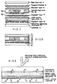
- FIGS 3 and 4 of the accompanying drawings show a reflection-mode diffractive spatial light modulator (SLM) of the type disclosed in GB 9611993.8 (publication No. 2 313 920).
- the SLM comprises a rectangular array of rectangular or substantially rectangular picture elements, only one of which is shown in Figures 3 and 4.
- the SLM comprises upper and lower glass substrates 11 and 12.
- the upper substrate 11 is coated with a transparent conducting layer of indium tin oxide (ITO) which is etched to form elongate interdigitated electrodes 13.
- the electrodes 13 are covered with an alignment layer 14 for a ferroelectric liquid crystal material.
- ITO indium tin oxide
- a combined mirror and electrode 15 is formed on the glass substrate 12 and a static quarterwave plate 16 is formed on the silver mirror and electrode 15.
- the thickness of the plate 16 is controlled so that it acts as a quarterwave plate for a predetermined bandwidth in the visible spectrum, for instance centred about 633 nanometres.
- a further alignment layer 17 is formed on the quarterwave plate 16.
- the substrates 11 and 12 are then spaced apart and stuck together so as to form a cell which is filled with the ferroelectric liquid crystal material to form a layer 18.
- the spacing provides a layer of ferroelectric liquid crystal material which provides a halfwave of retardation so that the liquid crystal layer acts as a halfwave retarder whose optic axis is switchable as described hereinafter.
- the electrode 15 acts as a common electrode which is connectable to a reference voltage line, for instance supplying zero volts, for strobing data to be displayed at the pixel.
- Alternate ones of the elongate electrodes 13 are connected together to form first and second sets of parallel interdigitated electrodes which are connected to receive suitable data signals.
- Each pixel is switchable between a reflective state and a diffractive state as described hereinafter.
- Figure 5 of the accompanying drawings illustrates diagrammatically the operation of adjacent strips of the pixel shown in Figures 3 and 4 when the pixel is in the diffractive mode.
- the optical path through each pixel is folded by reflection at the mirror 15 but, for the sake of clarity, the path is shown unfolded in Figure 5.
- the SLM acts on unpolarised light, which may be split into components of orthogonal polarisations for the sake of describing operation of the SLM.
- One of the component polarisations is shown at 20 in Figure 5 and is at an angle - ⁇ with respect to a predetermined direction 21.
- ferroelectric liquid crystal material strips 18a and 18b disposed between the electrodes 13a and 13b and the electrode 15 have optic axes aligned at angles of - ⁇ and + ⁇ , respectively, with respect to the direction 21, where ⁇ is preferably approximately equal to 22.5 degrees.
- Each strip 18a of ferroelectric liquid crystal material acts as a halfwave retarder so that the polarisation of the light component leaving the strip 18a is at an angle of ⁇ -2 ⁇ with respect to the direction 21.
- the light component then passes through the static quarterwave plate 16, is reflected by the mirror 15, and again passes through the static quarterwave plate 16, so that the combination of the quarterwave plate 16 and the mirror 15 acts as a halfwave retarder whose optic axis is parallel to the direction 21.
- the polarisation direction of light leaving the quarterwave plate 16 and travelling towards the ferroelectric liquid crystal material is "reflected" about the optic axis of the quarterwave plate and thus forms an angle 2 ⁇ - ⁇ with respect to the direction 21.
- the light component then again passes through the strip 18a of ferroelectric liquid crystal material so that the output polarisation as shown at 24 is at an angle of ⁇ -4 ⁇ with respect to the direction 21.
- the optical path through the SLM via each of the strips 18a of ferroelectric liquid crystal material is such that the polarisation direction is rotated by -4 ⁇ .
- This optical path therefore rotates the polarisation of unpolarised light by -4 ⁇ , which is substantially equal to -90 degrees.
- Each strip 18b of ferroelectric liquid crystal material acts as a halfwave retarder and rotates the polarisation direction to ⁇ +2 ⁇ .
- the fixed halfwave retarder formed by the combination of the quarterwave plate 16 and the mirror 15 rotates the direction of polarisation of the light component so that it makes an angle of -2 ⁇ - ⁇ with respect to the direction 21.
- the final passage through the strip 18b rotates the polarisation direction to ⁇ +4 ⁇ as shown at 25.
- Light of the orthogonal polarisation has its polarisation rotated in the same way.
- unpolarised light passing through the strips 18b has its polarisation rotated by +4 ⁇ , which is substantially equal to +90 degrees.
- each of the strips 18b is out of phase by 180 degrees with respect to light passing through each of the strips 18a when the electrodes 13b and 13a are connected to receive data signals of opposite polarity.
- the pixel acts as a phase-only diffraction grating and the pixel operates in the diffractive mode. Because of the bistable characteristics of ferroelectric liquid crystals, it is necessary only to supply the data signals in order to switch the strips 18a and 18b to the different modes illustrated in Figure 5.
- each pixel is therefore switchable between a transmissive mode, in which light is specularly reflected or "diffracted" into the zeroth diffraction order, and a diffractive mode, in which light incident on the pixel is diffracted into the non-zero diffraction orders.
- Such a diffractive SLM can be used with unpolarised light and provides increased optical modulation efficiency compared with SLMs which require polarised light.
- FIG. 6 of the accompanying drawings illustrates a projection display using an SLM 30 of the type shown in Figures 3 and 4.
- the SLM 30 is illuminated by an unpolarised light source 31 via a mirror 32.
- a projection optical system 33 projects an image displayed by the SLM 30 onto a screen 34.
- Each pixel which is in the reflective mode reflects the incident light normally back to the mirror 32 so that the reflected light is not projected by the system 33.
- a "dark" pixel is imaged on the screen 34 by the system 33.
- Each pixel in the diffractive mode deflects the incident light into the non-zero diffraction orders, mainly into the positive and negative first orders as illustrated by light rays 35 and 36. The light from each such pixel is thus imaged to a "bright" pixel on the screen 34.
- a polarisation independent optical phase modulator comprising: two substrates; a reflector disposed between the two substrates; a waveplate disposed between a first of the substrates and the reflector for producing a retardation of (n+1) ⁇ /4, where n is an integer greater than or equal to zero and ⁇ is a predetermined wavelength of visible light, and having an optic axis; and a polarisation dependent electrooptic layer disposed between the waveplate and the first substrate for modulating the phase of light having a polarisation substantially at 45 degrees to the optic axis of the waveplate.
- a polarisation dependent electrooptic layer is a layer of electrooptic material which modulates the phase of light of a first linear polarisation as a function of an electric field applied to the layer but which does not affect the phase of light of a second linear polarisation orthogonal to the first polarisation.
- the same orthogonal polarisation states remain unaltered in amplitude on exiting the layer for all values of applied electric field.
- linear polarisation states aligned parallel and perpendicular to the alignment direction of the nematic liquid crystal are preserved. Only the linear polarisation state whose electric field is parallel to the long axis of the liquid crystal molecules is phase modulated as a function of the applied electric field.
- phase modulator When light is reflected by a phase modulator, according to the invention, one of two orthogonal polarisations is modulated by the electrooptic layer on its way to the reflector whereas the other is modulated after being reflected by the reflector.
- the waveplate and the reflector cooperate to form a waveplate which has a retardation of (n+1) ⁇ /2 which reflects the polarisations about the optic axis of the waveplate.
- modulation of the two polarisation states occurs with an optical separation substantially equal to twice the thickness of the waveplate.
- the optical path difference can be made of the order of the wavelength of light.
- optical phase modulator is used with unpolarised incoherent light sources, such as light emitting diodes and white light sources.
- Eschler uses the same mode of operation as the present invention, but has a different structure.
- Eschler discloses the use of individual separate elements.
- the structure of the present invention allows the effects of parallax to be reduced as described hereinbefore. Sharp imaging is possible so that high resolution devices can be provided.
- the structure of the present invention allows the second substrate to be embodied as an active substrate and a reflecting substrate. This gives the possibility of achieving high fill factors which improve the optical performance of the device.
- the structure disclosed by Eschler cannot be formed as a reflective addressed device using, for example, a silicon large scale integration (LSI) backplane.
- LSI silicon large scale integration
- phase modulation it is possible to provide continuous or analogue phase modulation as opposed to binary modes of operation in which, for instance, a diffraction grating can only be switched on or off.
- blazed gratings can be achieved for use where high fidelity single beam diffraction is required.
- grey scale can be achieved within each pixel, for instance in display applications.
- the same device may be used for different wavelengths.
- the wavelength for which the device is to be used merely determines the range of electric fields which must be applied to the electrooptic layer to achieve the desired range of phase modulation.
- the waveplate may comprise a layer of aligned and cured reactive mesogen.
- the electrooptic layer may comprise a layer of liquid crystal arranged to perform out-of-plane switching.
- the liquid crystal may be a nematic liquid crystal.
- the liquid crystal has positive dielectric anisotropy and is disposed between alignment layers defining antiparallel alignment.
- the liquid crystal has positive dielectric anisotropy and is disposed between alignment layers defining parallel alignment.
- the liquid crystal has positive dielectric anisotropy and is disposed between alignment layers defining hybrid alignment, in which one of the substrates has parallel alignment and the other substrate has homeotropic alignment.
- the liquid crystal has negative dielectric anisotropy and is disposed between alignment layers defining homeotropic alignment.
- the liquid crystal has negative dielectric anisotropy and is disposed between mutually parallel alignment layers.
- the electrooptic layer may comprise a layer of lithium niobate.
- the modulator may comprise a plurality of picture elements, each of which has at least one transparent first electrode disposed between the first substrate and the electrooptic layer and at least one second electrode disposed between the second substrate and the electrooptic layer.
- the second electrodes may comprise the reflector.
- the first electrodes of all the picture elements may comprise a continuous layer of conductor.
- Each of the picture elements may have a plurality of first or second electrodes which are elongate and parallel.
- the substrate 12 carries reflecting addressing electrodes 15 in the form of parallel elongate strips, for instance formed by depositing aluminium to a thickness of approximately 100 nanometres and etching to form the desired electrode pattern.
- a static quarterwave plate 16 is formed on the alignment layer 19, for instance by spinning on a mixture of a reactive mesogen diacrylate, such as that known as RM258 available from Merck in Poole, UK, in a suitable solvent such a chlorobenzine with a photoinitiator.
- the alignment layer 19 aligns the reactive mesogen, which is then cured for approximately ten minutes under ultraviolet light in an atmosphere of nitrogen.
- the thickness of the plate 16 is controlled, for instance by varying the mixed ratios of the materials and the spin speed, so that it acts as a quarterwave plate for a predetermined bandwidth in the visible spectrum, for instance centred about 633 nanometres.
- the quarterwave plate 16 therefore typically has a thickness of the order of 800 nanometres.
- a further alignment layer 17 is formed on the quarterwave plate 16, for instance as described hereinbefore for the alignment layer 14.
- the alignment layers 14 and 17 are spun onto the underlying surface and comprise a polyimide material which is then rubbed at 45 degrees relative to the alignment direction of the plate 16. The rubbing directions of the alignment layers 14 and 17 are opposite so as to provide antiparallel alignment.
- the substrates 11 and 12 are then spaced apart, for instance by spacer balls, and stuck together so as to form a cell which is filled with nematic liquid crystal material to form a layer 18.
- the nematic liquid crystal material may be that known as E7 available from Merck in Poole, UK.
- the thickness of the layer 18 is required to be such that the retardation provided by the layer can be controlled over a desired range for an acceptable range of voltages applied between the electrodes 13 and 15 and is typically between 1.5 and 2.5 micrometres.
- the reflectivity of each interface should preferably be reduced, for instance by applying antireflection coatings to the substrate 11.
- the use of antiparallel alignment with a nematic liquid crystal for the layer 18 of positive dielectric anisotropy results in the formation of a Freedericksz cell arrangement.
- the nematic liquid crystal forms, in the absence of an applied electric field, a nearly uniform parallel aligned layer whose optic axis, which is parallel to the long molecular axis, is at a small angle from the plane of the cell surface. The small angle is determined by the pretilt induced by the alignment layers 14 and 17.
- Figure 9 is a simplified cross-sectional view of the modulator illustrated in Figures 7 and 8 illustrating the effects of applying different magnitudes of electric field across the layer 18.
- the application of an electric field by supplying a suitable potential difference between the electrodes 13 and 15 forces the liquid crystal molecules to rotate out of the cell plane. This results in changes to the refractive index seen by light polarised along the alignment direction of the liquid crystal.
- Optical propagation through regions of the layer 18 with different applied fields and therefore different out-of-plane liquid crystal molecular orientations results in spatially varying analogue phase modulation and hence in diffraction.
- the quarterwave plate 16 and the reflector formed by the electrodes 15 act as a halfwave plate which exchanges the polarisation directions of orthogonally polarised components of the incident light.
- subsequent propagation through the layer 18 results in the same modulation being applied to the orthogonal component, as described hereinbefore with reference to Figure 1.
- the modulator therefore acts as a polarisation independent optical phase modulator for all incident light.
- Figure 9 shows the effects of applying different voltages V1, V2 and V3 to the electrodes 15 relative to the electrode 13 on the long molecular axes of the nematic liquid crystal.
- V3 is a relatively low voltage and has little effect on the axes as illustrated in the region 40 of the layer 18.
- the voltage V2 is larger than V3 and results in tilting of the axes further away from the plane of the cell as illustrated in the region 41 of the layer 18.
- Application of a voltage V1 which is larger than V2 causes the molecular axes to be tilted such that they are substantially perpendicular to the cell surfaces as illustrated in the region 42 of the layer 18.
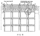
- Figure 10 illustrates an active matrix addressing arrangement for an optical phase modulator comprising a rectangular array of pixels of the type shown in Figures 7 to 9.
- This arrangement may be formed as an active backplane constituting the substrate 12 but with the positions of the "plane" electrodes 13 and the interdigitated electrodes 15 exchanged compared with Figures 7 to 9.
- the top substrate 11 carries two sets of interdigitated transparent electrodes 13, for instance made of indium tin oxide (ITO).
- the electrodes 13 are elongate or strip-shaped and are parallel with each other.
- the electrodes of each set are connected together and are interdigitated with the electrodes of the other set so that only two connections are required to the top substrate 11.
- the bottom substrate 12 carries a rectangular array of reflecting pixel electrodes such as that shown at 15.
- Each pixel electrode 15 faces a plurality of the interdigitated transparent electrodes 13.
- An active matrix addressing scheme is provided for individually controlling the pixel electrodes 15 and a pixel element of the addressing arrangement is shown diagrammatically to an enlarged scale at 61.
- each pixel electrode 15 is connected to the source of a thin film transistor (TFT) in the form of a pixel field effect transistor (FET).
- TFT thin film transistor
- FET pixel field effect transistor
- the pixels are arranged as rows and columns with the drains of the transistors of each column being connected to a respective column or data electrode 62 connected to a data signal generator (not shown) and the gates of the transistors of each row being connected to a respective row or scan electrode 63 connected to a strobe signal generator (not shown).
- the pixels are thus enabled one row at a time so that image data for a complete row are written simultaneously.
- the addressing arrangement illustrated schematically in Figure 10 is thus of the conventional dynamic random access memory (DRAM) type and may be fabricated on a silicon bottom substrate.
- the addressing arrangement may thus be substantially conventional and may be fabricated using substantially conventional techniques.
- the interdigitated electrodes are disposed on the bottom substrate 12 and may be reflective.
- the actively addressed optical phase modulator shown in Figure 10 is particularly suitable for use in projection display systems, for instance as illustrated in Figure 6 or in a Schlieren optical projection system, for instance as disclosed in "Schlicren Optical System Using Liquid Crystal Phase Gratings for Large Screen Projection, M.W. Fritsch, Displays, Vol. 13, No. 1, pp 45-60, 1992.
- the voltages applied to the electrodes 13 and 15 are such as to cause each pixel to act as a phase-only diffraction grating.
- the diffraction produced by the pixel is a maximum whereas, when there is zero phase shift between adjacent regions 18a and 18b, the pixel effectively ceases to operate as a diffraction grating.
- the two sets of interdigitated electrodes 13 are arranged to receive different voltages Va and Vb, for example 0 and 10 volts.
- the voltage Vc applied to each pixel electrode 15 is varied so as to control the diffraction, and hence the grey level, produced by the pixel.
- the pixel acts as a diffractive grating producing maximum diffraction.
- the voltage Vc is substantially midway between the voltages Va and Vb, for example 5 volts, the grating is "erased" and the pixel produces minimum diffraction.
- Intermediate voltages give varying diffraction to produce the intermediate grey levels.
- phase modulator in such an application is that it is capable of achieving grey levels.
- the pixel acts as a diffraction grating of variable diffraction efficiency.
- the amount of light diffracted away from the zeroth order can be varied by varying the signals supplied to the electrodes 15 with respect to the signals supplied to the electrode 13.
- phase modulators include beam steering, for instance as required for optical printing, and adaptive optics, for instance for focusing a source of light onto a plane whose distance varies as a function of time and/or position, for example in optical scanners.
- dislocations in the liquid crystal occur such as those shown ringed at 67. Such dislocations act as scattering defects and give rise to polarisation mixing and non-preservation of the polarisation states.
- the alignment 65 of the molecules is at an angle between zero and 90 degrees with respect to the longitudinal axes of the electrodes 15.
- a spacer layer may be disposed between the electrodes 15 and the nematic liquid crystal. This results in the field at the surface of the liquid crystal layer adjacent the electrodes 15 becoming lower in magnitude and more perpendicular to the surfaces of the liquid crystal layer so as to reduce the likelihood of dislocation formation.
- Figure 15 illustrates homeotropic alignment for a nematic liquid crystal material having negative dielectric anisotropy.
- the nematic liquid crystal molecules are aligned substantially normal to the surfaces of the cell with a slight tilt in a predetermined direction.
- the molecules attempt to rotate such that their long axes are normal to the field as illustrated in the left hand part of Figure 15. This results in a similar phase modulation as described hereinbefore but with opposite dependency on the applied field.
- Figure 16 illustrates a ⁇ -cell alignment in which a positive dielectric anisotropy nematic liquid crystal is used with parallel (as opposed to antiparallel) alignment, for instance by using alignment layers 14 and 17 which are rubbed in the same direction.
- This alignment causes the nematic liquid crystal to form two possible relaxed states.
- the V-state is favoured and can be made to switch in a similar way to the Freedericksz cell but with a faster response time.
- Figure 17 illustrates another example of out-of-plane nematic liquid crystal switching known as the hybrid aligned nematic or HAN structure, in which one surface is planar aligned and the other is homeotropically aligned as shown in the right hand part of Figure 17.
- the resulting liquid crystal layer 18 has to be approximately twice as thick as for the arrangements shown in Figures 14 to 16 because of the out-of-plane switching present in part of the layer in the relaxed state.
- an advantage of this alignment is that no brushing or equivalent for planar alignment is required on one of the cell surfaces.
- Figure 18 illustrates another example of out-of-plane nematic liquid crystal switching known as the splayed birefringent device (SBD) mode, which is described in WO97/12275.
- a nematic liquid crystal layer 18 is disposed between first and second mutually parallel alignment layers (not shown).
- the alignment layers inpart a high surface pre-tilt (preferably around 80 - 90°) to liquid crystal molecules in surface regions of the liquid crystal layer 18.
- the nematic liquid crystal layer 18 has a negative dielectric anisotropy, so the liquid crystal molecules prefer to align themselves with their short axes parallel to an applied electric field.
- the liquid crystal molecules in the layer 18 adopt a bend configuration across the thickness of the layer 18.
- the liquid crystal molecules realign themselves to lie with their short axes along the direction of the applied field so as to produce a splay state.
- the birefringence of the liquid crystal layer 18 increases.
- the electrooptic material may comprise lithium niobate.
- Achromatic waveplate techniques may be used in the present devices. For instance, such techniques are disclosed in Pancharatnum et al, Proc. Ind. Acad. Sci, 1955, 41A, 130 and 137 "Achromatic Combinations of Birefringent Plates".
- the devices can be made to operate at different wavelengths by using a "static" achromatic waveplate 16 and by tuning the driving voltage and hence the field applied to the electrooptic material.
- three identical such modulators may be used for modulating red, green and blue light with the applied voltages to each devices being selected to optimise performance for the colour which it is required to modulate.
- phase modulators for a colour projection display using phase modulators of the present type, three identical such modulators may be used for modulating red, green and blue light with the applied voltages to each devices being selected to optimise performance for the colour which it is required to modulate.
- only a single device needs to be manufactured so that costs may be reduced.
Landscapes
- Physics & Mathematics (AREA)
- Nonlinear Science (AREA)
- General Physics & Mathematics (AREA)
- Optics & Photonics (AREA)
- Chemical & Material Sciences (AREA)
- Crystallography & Structural Chemistry (AREA)
- Mathematical Physics (AREA)
- Liquid Crystal (AREA)
- Polarising Elements (AREA)
- Optical Integrated Circuits (AREA)
Applications Claiming Priority (2)
| Application Number | Priority Date | Filing Date | Title |
|---|---|---|---|
| GB9709467 | 1997-05-09 | ||
| GB9709467A GB2325056A (en) | 1997-05-09 | 1997-05-09 | Polarisation independent optical phase modulator |
Publications (3)
| Publication Number | Publication Date |
|---|---|
| EP0878729A2 true EP0878729A2 (de) | 1998-11-18 |
| EP0878729A3 EP0878729A3 (de) | 1999-03-24 |
| EP0878729B1 EP0878729B1 (de) | 2006-09-27 |
Family
ID=10812082
Family Applications (1)
| Application Number | Title | Priority Date | Filing Date |
|---|---|---|---|
| EP98303574A Expired - Lifetime EP0878729B1 (de) | 1997-05-09 | 1998-05-07 | Polarisationsunabhängiger optischer Phasenmodulator |
Country Status (6)
| Country | Link |
|---|---|
| US (1) | US5973817A (de) |
| EP (1) | EP0878729B1 (de) |
| JP (1) | JP3512150B2 (de) |
| KR (1) | KR100263210B1 (de) |
| DE (1) | DE69835976T2 (de) |
| GB (1) | GB2325056A (de) |
Cited By (6)
| Publication number | Priority date | Publication date | Assignee | Title |
|---|---|---|---|---|
| WO2001025840A1 (en) * | 1999-10-04 | 2001-04-12 | Thomas Swan & Co. Ltd. | Optical switch |
| FR2825805A1 (fr) * | 2001-06-07 | 2002-12-13 | France Telecom | Dispositif de raccordement hybride entre fibres optiques et lignes transportant des signaux electriques, et reseaux incorportant ce dispositif |
| FR2851055A1 (fr) * | 2003-02-12 | 2004-08-13 | Optogone Sa | Dispositif de modulation spatiale d'un faisceau lumineux, et applications correspondantes |
| WO2008003004A3 (en) * | 2006-06-27 | 2008-02-21 | Solbeam Inc | Electro-optic reflective beam-steering or focussing assembly, and solar energy conversion system |
| US8937759B2 (en) | 2001-09-03 | 2015-01-20 | Thomas Swan & Co. Ltd. | Optical processing |
| US10257594B2 (en) | 2012-08-15 | 2019-04-09 | Thomas Swan And Co., Ltd. | Optical device and methods |
Families Citing this family (41)
| Publication number | Priority date | Publication date | Assignee | Title |
|---|---|---|---|---|
| GB2315902A (en) * | 1996-08-01 | 1998-02-11 | Sharp Kk | LIquid crystal device |
| GB9704623D0 (en) * | 1997-03-06 | 1997-04-23 | Sharp Kk | Liquid crytal optical element and liquid crystal device incorporating same |
| JP3063843B2 (ja) * | 1997-12-02 | 2000-07-12 | 日本電気株式会社 | 液晶初期配向角測定法及び液晶初期配向角測定装置 |
| US6151154A (en) * | 1998-03-12 | 2000-11-21 | Pioneer Electronic Corporation | Optical pickup, aberration correction unit and astigmatism measurement method |
| GB2345978A (en) * | 1999-01-23 | 2000-07-26 | Sharp Kk | Diffractive spatial light modulator |
| US20040111219A1 (en) * | 1999-02-22 | 2004-06-10 | Sandeep Gulati | Active interferometric signal analysis in software |
| JP2002542513A (ja) * | 1999-04-20 | 2002-12-10 | コーニンクレッカ フィリップス エレクトロニクス エヌ ヴィ | 透過/反射切換え型表示装置 |
| EP2506090B1 (de) * | 2000-05-30 | 2016-12-07 | Dai Nippon Printing Co., Ltd. | Computererzeugtes Hologramm, Reflektor mit einem computererzeugten Hologramm und reflektierende Flüssigkristallanzeige |
| JP2002074727A (ja) * | 2000-09-01 | 2002-03-15 | Samsung Electro Mech Co Ltd | ダイナミック制御回折格子並びに情報記録再生装置と情報再生装置 |
| US6456419B1 (en) * | 2000-09-29 | 2002-09-24 | Innovative Technology Licensing, Llc | Frequency modulated liquid crystal beamsteering device |
| US6490076B2 (en) * | 2001-01-11 | 2002-12-03 | Hrl Laboratories, Llc | Optical phased array for depolarized optical beam control |
| US20040208436A1 (en) * | 2002-01-16 | 2004-10-21 | Teraphase Technologies, Inc. | Forming optical signals having soliton pulses with certain spectral band characteristics |
| US20040208651A1 (en) * | 2002-05-23 | 2004-10-21 | Farhad Hakimi | Optical signal receiver |
| US20030228095A1 (en) * | 2002-06-10 | 2003-12-11 | Farhad Hakimi | System for and method of replicating optical pulses |
| US20040208627A1 (en) * | 2002-08-02 | 2004-10-21 | Farhad Hakimi | Optical signal transmission method |
| SE0303041D0 (sv) * | 2003-06-23 | 2003-11-18 | Ecsibeo Ab | A liquid crystal device and a method for manufacturing thereof |
| JP2005181965A (ja) * | 2003-11-25 | 2005-07-07 | Ricoh Co Ltd | 空間光変調器及び表示装置及び投射表示装置 |
| CN100437207C (zh) * | 2004-03-31 | 2008-11-26 | 松下电器产业株式会社 | 颜色分离装置及摄像装置 |
| US20050232530A1 (en) * | 2004-04-01 | 2005-10-20 | Jason Kekas | Electronically controlled volume phase grating devices, systems and fabrication methods |
| US7317568B2 (en) * | 2004-09-27 | 2008-01-08 | Idc, Llc | System and method of implementation of interferometric modulators for display mirrors |
| US7583429B2 (en) | 2004-09-27 | 2009-09-01 | Idc, Llc | Ornamental display device |
| KR101170911B1 (ko) * | 2005-06-30 | 2012-08-03 | 엘지디스플레이 주식회사 | 광시야각과 협시야각의 모드전환이 가능한 액정표시장치 및그 제조방법 |
| KR101122199B1 (ko) * | 2005-07-07 | 2012-03-19 | 삼성전자주식회사 | 2차원/3차원 영상 호환용 입체영상 디스플레이 장치 |
| US8570460B2 (en) * | 2005-12-19 | 2013-10-29 | Kent State University | Electronically-controllable polarization independent liquid crystal optical medium and devices using same |
| DE102006060604A1 (de) * | 2006-12-21 | 2008-06-26 | Leopold Kostal Gmbh & Co. Kg | Photoelektrische Sensoreinrichtung |
| JP4201054B2 (ja) * | 2007-02-16 | 2008-12-24 | 凸版印刷株式会社 | カラーフィルタ及びその製造方法及び液晶表示装置 |
| JP4211872B2 (ja) * | 2007-02-16 | 2009-01-21 | 凸版印刷株式会社 | カラーフィルタ及びその製造方法及び液晶表示装置 |
| JP5100309B2 (ja) * | 2007-10-25 | 2012-12-19 | 株式会社ジャパンディスプレイウェスト | 液晶装置の製造方法 |
| JP5270142B2 (ja) | 2007-12-05 | 2013-08-21 | 浜松ホトニクス株式会社 | 反射型空間光変調素子 |
| US8077326B1 (en) | 2008-03-31 | 2011-12-13 | Qualcomm Mems Technologies, Inc. | Human-readable, bi-state environmental sensors based on micro-mechanical membranes |
| US7852491B2 (en) | 2008-03-31 | 2010-12-14 | Qualcomm Mems Technologies, Inc. | Human-readable, bi-state environmental sensors based on micro-mechanical membranes |
| US8711361B2 (en) * | 2009-11-05 | 2014-04-29 | Qualcomm, Incorporated | Methods and devices for detecting and measuring environmental conditions in high performance device packages |
| CN102725683B (zh) * | 2009-12-01 | 2016-02-24 | 视瑞尔技术公司 | 用于调制与相位调制器相互作用的光的相位调制器 |
| DE102010064383B4 (de) * | 2010-12-22 | 2015-10-29 | Seereal Technologies S.A. | Lichtmodulationseinrichtung |
| KR20160068113A (ko) * | 2014-12-04 | 2016-06-15 | 삼성디스플레이 주식회사 | 광 변조 장치를 포함하는 광학 장치 및 그 구동 방법 |
| US10466551B2 (en) * | 2016-07-13 | 2019-11-05 | Research & Business Foundation Sungkyunkwan University | Wavelength-tunable type etalon comprising LCD-layer and preparation method thereof |
| TWI647513B (zh) | 2017-10-20 | 2019-01-11 | 國立交通大學 | 偏振無關液晶相位調制器 |
| KR102070349B1 (ko) * | 2019-04-17 | 2020-01-28 | 광운대학교 산학협력단 | 리튬나이오베이트-실리콘나이트라이드 기반의 광 위상변조기 및 이를 이용한 광위상 배열안테나 |
| CN110068945B (zh) * | 2019-05-10 | 2021-03-30 | 中国科学院长春光学精密机械与物理研究所 | 一种反射式复合液晶偏振光栅及其制备方法 |
| GB2587400B (en) * | 2019-09-27 | 2022-02-16 | Dualitas Ltd | Hologram display using a liquid crystal display device |
| JP7474126B2 (ja) * | 2020-06-17 | 2024-04-24 | 浜松ホトニクス株式会社 | 画像出力装置 |
Family Cites Families (18)
| Publication number | Priority date | Publication date | Assignee | Title |
|---|---|---|---|---|
| US3912369A (en) * | 1974-07-02 | 1975-10-14 | Gen Electric | Single polarizer reflective liquid crystal display |
| US4266859A (en) * | 1977-10-14 | 1981-05-12 | Citizen Watch Co., Ltd. | Liquid crystal display device |
| JPS54139569A (en) * | 1978-04-20 | 1979-10-30 | Matsushita Electric Ind Co Ltd | Light bulb type projector |
| JP2569645B2 (ja) * | 1987-12-07 | 1997-01-08 | キヤノン株式会社 | 反射型光変調装置 |
| US5182665A (en) * | 1990-09-07 | 1993-01-26 | Displaytech, Inc. | Diffractive light modulator |
| JP2656666B2 (ja) * | 1990-12-27 | 1997-09-24 | キヤノン株式会社 | 投射型表示装置 |
| DE69229843T2 (de) * | 1991-04-23 | 2000-01-13 | Seiko Instr Inc | Optisches Mustererkennungssystem und Ansteuerverfahren für räumlichen Lichtmodulator mit ferroelektrischen, flüssigen Kristallen |
| JPH0511281A (ja) * | 1991-07-05 | 1993-01-19 | Matsushita Electric Ind Co Ltd | 液晶パネルおよびそれを用いた液晶投写型テレビ |
| JP3058378B2 (ja) * | 1992-10-27 | 2000-07-04 | 松下電器産業株式会社 | 液晶パネル及びそれを用いた液晶投写型テレビ |
| JP3276745B2 (ja) * | 1993-11-15 | 2002-04-22 | 株式会社日立製作所 | 可変波長発光素子とその制御方法 |
| GB2287327A (en) * | 1994-03-02 | 1995-09-13 | Sharp Kk | Electro-optic apparatus |
| GB2292814A (en) * | 1994-09-01 | 1996-03-06 | Sharp Kk | Liquid crystal display |
| JPH08106087A (ja) * | 1994-10-05 | 1996-04-23 | Fuji Xerox Co Ltd | 反射型液晶表示装置 |
| JP3393458B2 (ja) * | 1995-07-19 | 2003-04-07 | ソニー株式会社 | 反射型ゲストホスト液晶表示装置 |
| JPH0990431A (ja) * | 1995-09-19 | 1997-04-04 | Sony Corp | 反射型ゲストホスト液晶表示装置 |
| AU7095996A (en) * | 1995-09-26 | 1997-04-17 | Chisso Corporation | Homeotropic sprayed-nematic liquid crystal display device |
| JPH09197388A (ja) * | 1996-01-11 | 1997-07-31 | Alps Electric Co Ltd | 反射型液晶表示装置 |
| GB2313920A (en) * | 1996-06-07 | 1997-12-10 | Sharp Kk | Diffractive spatial light modulator and display |
-
1997
- 1997-05-09 GB GB9709467A patent/GB2325056A/en not_active Withdrawn
-
1998
- 1998-05-07 EP EP98303574A patent/EP0878729B1/de not_active Expired - Lifetime
- 1998-05-07 DE DE69835976T patent/DE69835976T2/de not_active Expired - Lifetime
- 1998-05-08 JP JP12653998A patent/JP3512150B2/ja not_active Expired - Fee Related
- 1998-05-08 US US09/074,858 patent/US5973817A/en not_active Expired - Lifetime
- 1998-05-09 KR KR1019980016651A patent/KR100263210B1/ko not_active Expired - Fee Related
Cited By (13)
| Publication number | Priority date | Publication date | Assignee | Title |
|---|---|---|---|---|
| WO2001025840A1 (en) * | 1999-10-04 | 2001-04-12 | Thomas Swan & Co. Ltd. | Optical switch |
| US6954252B1 (en) | 1999-10-04 | 2005-10-11 | Thomas Swan & Co. Ltd | Optical switch including two integrated multiphase SLM's and a wave-plate the wave-plate providing an optical retardance of (2n+1)λ/4 |
| FR2825805A1 (fr) * | 2001-06-07 | 2002-12-13 | France Telecom | Dispositif de raccordement hybride entre fibres optiques et lignes transportant des signaux electriques, et reseaux incorportant ce dispositif |
| WO2002100007A3 (fr) * | 2001-06-07 | 2003-01-30 | France Telecom | Dispositif de raccordement hybride entre fibres optiques et lignes transportant des signaux electriques, et reseaux incorporant ce dispositif |
| US10180616B2 (en) | 2001-09-03 | 2019-01-15 | Thomas Swan & Co. Ltd. | Optical processing |
| US11073739B2 (en) | 2001-09-03 | 2021-07-27 | Thomas Swan & Co. Ltd. | Optical processing |
| US10642126B2 (en) | 2001-09-03 | 2020-05-05 | Thomas Swan & Co. Ltd. | Optical processing |
| US8937759B2 (en) | 2001-09-03 | 2015-01-20 | Thomas Swan & Co. Ltd. | Optical processing |
| US9529325B2 (en) | 2001-09-03 | 2016-12-27 | Thomas Swan & Co. Ltd | Optical processing |
| FR2851055A1 (fr) * | 2003-02-12 | 2004-08-13 | Optogone Sa | Dispositif de modulation spatiale d'un faisceau lumineux, et applications correspondantes |
| EP1447707A1 (de) * | 2003-02-12 | 2004-08-18 | Optogone | Vorrichtung zur räumlichen Modulation eines Lichtstrahls und entsprechende Anwendungen |
| WO2008003004A3 (en) * | 2006-06-27 | 2008-02-21 | Solbeam Inc | Electro-optic reflective beam-steering or focussing assembly, and solar energy conversion system |
| US10257594B2 (en) | 2012-08-15 | 2019-04-09 | Thomas Swan And Co., Ltd. | Optical device and methods |
Also Published As
| Publication number | Publication date |
|---|---|
| GB2325056A (en) | 1998-11-11 |
| KR100263210B1 (ko) | 2000-08-01 |
| DE69835976T2 (de) | 2007-05-24 |
| JPH10311975A (ja) | 1998-11-24 |
| EP0878729A3 (de) | 1999-03-24 |
| JP3512150B2 (ja) | 2004-03-29 |
| KR19980086903A (ko) | 1998-12-05 |
| GB9709467D0 (en) | 1997-07-02 |
| US5973817A (en) | 1999-10-26 |
| DE69835976D1 (de) | 2006-11-09 |
| EP0878729B1 (de) | 2006-09-27 |
Similar Documents
| Publication | Publication Date | Title |
|---|---|---|
| EP0878729B1 (de) | Polarisationsunabhängiger optischer Phasenmodulator | |
| US6243063B1 (en) | Diffractive spatial light modulator and display | |
| US6373549B1 (en) | Diffractive spatial light modulator and display | |
| US5986740A (en) | Liquid crystal diffractive spatial light modulator and display having two switchable retarders and one passive retarder | |
| US6310664B1 (en) | Continuously viewable, DC field-balanced, reflective, ferroelectric liquid crystal image generator | |
| US6281866B1 (en) | Display device and a method of addressing a display device | |
| US5825448A (en) | Reflective optically active diffractive device | |
| EP0448124B1 (de) | Optische Modulationsvorrichtung und Anzeigegerät | |
| US5973759A (en) | Liquid crystal projector | |
| US6593987B1 (en) | Multi-domain surface mode device | |
| EP1050775A1 (de) | Optischer Phasenmodulator | |
| US6201589B1 (en) | Spatial light modulator and display with picture elements having electrically floating electrodes | |
| US6924870B1 (en) | Liquid crystal on silicon diffractive light valve | |
| JP3557313B2 (ja) | 液晶表示スクリーン | |
| JPH05119341A (ja) | 光学装置 | |
| KR100434970B1 (ko) | 액정표시장치 | |
| Hu et al. | Modulating both amplitude and phase in a single-spatial light modulator (SLM) | |
| JP2871083B2 (ja) | 液晶空間光変調素子および光学的画像処理装置 | |
| Holton et al. | Patterned alignment liquid-crystal diffractive spatial light modulators and devices | |
| Medialdea | Nearly-analogue blazed phase grating using high birefringence liquid crystal | |
| JPH1152360A (ja) | 液晶表示素子 | |
| Lagerwall et al. | Liquid Crystals: Electro-Optical Modes and Applications | |
| JPH03264918A (ja) | 反射型位相変調素子および光情報処理装置 | |
| HK1016274A (en) | Liquid crystal projector | |
| JPH1152358A (ja) | 液晶表示素子 |
Legal Events
| Date | Code | Title | Description |
|---|---|---|---|
| PUAI | Public reference made under article 153(3) epc to a published international application that has entered the european phase |
Free format text: ORIGINAL CODE: 0009012 |
|
| AK | Designated contracting states |
Kind code of ref document: A2 Designated state(s): DE FR GB |
|
| AX | Request for extension of the european patent |
Free format text: AL;LT;LV;MK;RO;SI |
|
| PUAL | Search report despatched |
Free format text: ORIGINAL CODE: 0009013 |
|
| AK | Designated contracting states |
Kind code of ref document: A3 Designated state(s): AT BE CH CY DE DK ES FI FR GB GR IE IT LI LU MC NL PT SE |
|
| AX | Request for extension of the european patent |
Free format text: AL;LT;LV;MK;RO;SI |
|
| 17P | Request for examination filed |
Effective date: 19990806 |
|
| AKX | Designation fees paid |
Free format text: DE FR GB |
|
| 17Q | First examination report despatched |
Effective date: 20050503 |
|
| GRAP | Despatch of communication of intention to grant a patent |
Free format text: ORIGINAL CODE: EPIDOSNIGR1 |
|
| GRAC | Information related to communication of intention to grant a patent modified |
Free format text: ORIGINAL CODE: EPIDOSCIGR1 |
|
| RIC1 | Information provided on ipc code assigned before grant |
Ipc: G02F 1/139 20060101ALI20060202BHEP Ipc: G02F 1/29 20060101ALI20060202BHEP Ipc: G02F 1/1335 20060101AFI20060202BHEP |
|
| GRAS | Grant fee paid |
Free format text: ORIGINAL CODE: EPIDOSNIGR3 |
|
| GRAA | (expected) grant |
Free format text: ORIGINAL CODE: 0009210 |
|
| AK | Designated contracting states |
Kind code of ref document: B1 Designated state(s): DE FR GB |
|
| REG | Reference to a national code |
Ref country code: GB Ref legal event code: FG4D |
|
| REF | Corresponds to: |
Ref document number: 69835976 Country of ref document: DE Date of ref document: 20061109 Kind code of ref document: P |
|
| ET | Fr: translation filed | ||
| PLBE | No opposition filed within time limit |
Free format text: ORIGINAL CODE: 0009261 |
|
| STAA | Information on the status of an ep patent application or granted ep patent |
Free format text: STATUS: NO OPPOSITION FILED WITHIN TIME LIMIT |
|
| 26N | No opposition filed |
Effective date: 20070628 |
|
| PGFP | Annual fee paid to national office [announced via postgrant information from national office to epo] |
Ref country code: GB Payment date: 20130501 Year of fee payment: 16 Ref country code: DE Payment date: 20130515 Year of fee payment: 16 |
|
| PGFP | Annual fee paid to national office [announced via postgrant information from national office to epo] |
Ref country code: FR Payment date: 20130531 Year of fee payment: 16 |
|
| REG | Reference to a national code |
Ref country code: DE Ref legal event code: R119 Ref document number: 69835976 Country of ref document: DE |
|
| GBPC | Gb: european patent ceased through non-payment of renewal fee |
Effective date: 20140507 |
|
| REG | Reference to a national code |
Ref country code: DE Ref legal event code: R119 Ref document number: 69835976 Country of ref document: DE Effective date: 20141202 |
|
| REG | Reference to a national code |
Ref country code: FR Ref legal event code: ST Effective date: 20150130 |
|
| PG25 | Lapsed in a contracting state [announced via postgrant information from national office to epo] |
Ref country code: DE Free format text: LAPSE BECAUSE OF NON-PAYMENT OF DUE FEES Effective date: 20141202 |
|
| PG25 | Lapsed in a contracting state [announced via postgrant information from national office to epo] |
Ref country code: GB Free format text: LAPSE BECAUSE OF NON-PAYMENT OF DUE FEES Effective date: 20140507 Ref country code: FR Free format text: LAPSE BECAUSE OF NON-PAYMENT OF DUE FEES Effective date: 20140602 |