EP0878789A2 - Dispositif d'affichage - Google Patents
Dispositif d'affichage Download PDFInfo
- Publication number
- EP0878789A2 EP0878789A2 EP98410051A EP98410051A EP0878789A2 EP 0878789 A2 EP0878789 A2 EP 0878789A2 EP 98410051 A EP98410051 A EP 98410051A EP 98410051 A EP98410051 A EP 98410051A EP 0878789 A2 EP0878789 A2 EP 0878789A2
- Authority
- EP
- European Patent Office
- Prior art keywords
- fet
- oxide layer
- gate electrode
- gate oxide
- bias
- Prior art date
- Legal status (The legal status is an assumption and is not a legal conclusion. Google has not performed a legal analysis and makes no representation as to the accuracy of the status listed.)
- Ceased
Links
- 239000003990 capacitor Substances 0.000 claims abstract description 18
- VYPSYNLAJGMNEJ-UHFFFAOYSA-N Silicium dioxide Chemical compound O=[Si]=O VYPSYNLAJGMNEJ-UHFFFAOYSA-N 0.000 description 16
- 229910021420 polycrystalline silicon Inorganic materials 0.000 description 14
- 238000000034 method Methods 0.000 description 13
- 230000008569 process Effects 0.000 description 13
- 239000006185 dispersion Substances 0.000 description 11
- QGZKDVFQNNGYKY-UHFFFAOYSA-N Ammonia Chemical compound N QGZKDVFQNNGYKY-UHFFFAOYSA-N 0.000 description 10
- 229910021417 amorphous silicon Inorganic materials 0.000 description 10
- BLRPTPMANUNPDV-UHFFFAOYSA-N Silane Chemical compound [SiH4] BLRPTPMANUNPDV-UHFFFAOYSA-N 0.000 description 8
- 229910052681 coesite Inorganic materials 0.000 description 8
- 229910052906 cristobalite Inorganic materials 0.000 description 8
- 239000000377 silicon dioxide Substances 0.000 description 8
- 229910052682 stishovite Inorganic materials 0.000 description 8
- 229910052905 tridymite Inorganic materials 0.000 description 8
- 238000010586 diagram Methods 0.000 description 7
- 238000005268 plasma chemical vapour deposition Methods 0.000 description 7
- 239000000758 substrate Substances 0.000 description 6
- BOTDANWDWHJENH-UHFFFAOYSA-N Tetraethyl orthosilicate Chemical compound CCO[Si](OCC)(OCC)OCC BOTDANWDWHJENH-UHFFFAOYSA-N 0.000 description 5
- 239000010409 thin film Substances 0.000 description 5
- 230000008859 change Effects 0.000 description 4
- 239000011159 matrix material Substances 0.000 description 4
- 239000007790 solid phase Substances 0.000 description 4
- GQPLMRYTRLFLPF-UHFFFAOYSA-N Nitrous Oxide Chemical compound [O-][N+]#N GQPLMRYTRLFLPF-UHFFFAOYSA-N 0.000 description 3
- 230000015556 catabolic process Effects 0.000 description 2
- 238000011109 contamination Methods 0.000 description 2
- 230000007547 defect Effects 0.000 description 2
- 238000006731 degradation reaction Methods 0.000 description 2
- 230000005669 field effect Effects 0.000 description 2
- 230000004304 visual acuity Effects 0.000 description 2
- 230000000694 effects Effects 0.000 description 1
- 238000004020 luminiscence type Methods 0.000 description 1
- 230000004048 modification Effects 0.000 description 1
- 238000012986 modification Methods 0.000 description 1
- 230000035945 sensitivity Effects 0.000 description 1
- 239000007787 solid Substances 0.000 description 1
- 230000003068 static effect Effects 0.000 description 1
Images


Classifications
-
- G—PHYSICS
- G09—EDUCATION; CRYPTOGRAPHY; DISPLAY; ADVERTISING; SEALS
- G09G—ARRANGEMENTS OR CIRCUITS FOR CONTROL OF INDICATING DEVICES USING STATIC MEANS TO PRESENT VARIABLE INFORMATION
- G09G3/00—Control arrangements or circuits, of interest only in connection with visual indicators other than cathode-ray tubes
- G09G3/20—Control arrangements or circuits, of interest only in connection with visual indicators other than cathode-ray tubes for presentation of an assembly of a number of characters, e.g. a page, by composing the assembly by combination of individual elements arranged in a matrix no fixed position being assigned to or needed to be assigned to the individual characters or partial characters
- G09G3/22—Control arrangements or circuits, of interest only in connection with visual indicators other than cathode-ray tubes for presentation of an assembly of a number of characters, e.g. a page, by composing the assembly by combination of individual elements arranged in a matrix no fixed position being assigned to or needed to be assigned to the individual characters or partial characters using controlled light sources
- G09G3/30—Control arrangements or circuits, of interest only in connection with visual indicators other than cathode-ray tubes for presentation of an assembly of a number of characters, e.g. a page, by composing the assembly by combination of individual elements arranged in a matrix no fixed position being assigned to or needed to be assigned to the individual characters or partial characters using controlled light sources using electroluminescent panels
- G09G3/32—Control arrangements or circuits, of interest only in connection with visual indicators other than cathode-ray tubes for presentation of an assembly of a number of characters, e.g. a page, by composing the assembly by combination of individual elements arranged in a matrix no fixed position being assigned to or needed to be assigned to the individual characters or partial characters using controlled light sources using electroluminescent panels semiconductive, e.g. using light-emitting diodes [LED]
- G09G3/3208—Control arrangements or circuits, of interest only in connection with visual indicators other than cathode-ray tubes for presentation of an assembly of a number of characters, e.g. a page, by composing the assembly by combination of individual elements arranged in a matrix no fixed position being assigned to or needed to be assigned to the individual characters or partial characters using controlled light sources using electroluminescent panels semiconductive, e.g. using light-emitting diodes [LED] organic, e.g. using organic light-emitting diodes [OLED]
- G09G3/3225—Control arrangements or circuits, of interest only in connection with visual indicators other than cathode-ray tubes for presentation of an assembly of a number of characters, e.g. a page, by composing the assembly by combination of individual elements arranged in a matrix no fixed position being assigned to or needed to be assigned to the individual characters or partial characters using controlled light sources using electroluminescent panels semiconductive, e.g. using light-emitting diodes [LED] organic, e.g. using organic light-emitting diodes [OLED] using an active matrix
- G09G3/3233—Control arrangements or circuits, of interest only in connection with visual indicators other than cathode-ray tubes for presentation of an assembly of a number of characters, e.g. a page, by composing the assembly by combination of individual elements arranged in a matrix no fixed position being assigned to or needed to be assigned to the individual characters or partial characters using controlled light sources using electroluminescent panels semiconductive, e.g. using light-emitting diodes [LED] organic, e.g. using organic light-emitting diodes [OLED] using an active matrix with pixel circuitry controlling the current through the light-emitting element
-
- H—ELECTRICITY
- H10—SEMICONDUCTOR DEVICES; ELECTRIC SOLID-STATE DEVICES NOT OTHERWISE PROVIDED FOR
- H10K—ORGANIC ELECTRIC SOLID-STATE DEVICES
- H10K59/00—Integrated devices, or assemblies of multiple devices, comprising at least one organic light-emitting element covered by group H10K50/00
- H10K59/10—OLED displays
- H10K59/12—Active-matrix OLED [AMOLED] displays
- H10K59/121—Active-matrix OLED [AMOLED] displays characterised by the geometry or disposition of pixel elements
- H10K59/1213—Active-matrix OLED [AMOLED] displays characterised by the geometry or disposition of pixel elements the pixel elements being TFTs
-
- G—PHYSICS
- G09—EDUCATION; CRYPTOGRAPHY; DISPLAY; ADVERTISING; SEALS
- G09G—ARRANGEMENTS OR CIRCUITS FOR CONTROL OF INDICATING DEVICES USING STATIC MEANS TO PRESENT VARIABLE INFORMATION
- G09G2300/00—Aspects of the constitution of display devices
- G09G2300/08—Active matrix structure, i.e. with use of active elements, inclusive of non-linear two terminal elements, in the pixels together with light emitting or modulating elements
- G09G2300/0809—Several active elements per pixel in active matrix panels
- G09G2300/0842—Several active elements per pixel in active matrix panels forming a memory circuit, e.g. a dynamic memory with one capacitor
-
- G—PHYSICS
- G09—EDUCATION; CRYPTOGRAPHY; DISPLAY; ADVERTISING; SEALS
- G09G—ARRANGEMENTS OR CIRCUITS FOR CONTROL OF INDICATING DEVICES USING STATIC MEANS TO PRESENT VARIABLE INFORMATION
- G09G2320/00—Control of display operating conditions
- G09G2320/02—Improving the quality of display appearance
- G09G2320/0233—Improving the luminance or brightness uniformity across the screen
Definitions
- the present invention relates to an image display device, in particular, relates to a high quality image display device suitable to an organic electronics luminescence (EL) display device.
- EL organic electronics luminescence
- An image display device using an organic EL element has lately been developed.
- each pixcel, or image cell, of an EL is coupled with a field effect transistor (FET) implemented by a thin film transistor (TFT) for controlling current supplied to said pixcel.
- FET field effect transistor
- TFT thin film transistor
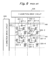
- Fig.9 shows a circuit diagram of a prior active matrix type organic EL display system.
- the system has a plurality of X-direction signal lines 301-1, 301-2, et al, a plurality of Y-direction signal lines 302-1, 302-2, et al, a plurality of power supply lines (Vdd) 303-1, 303-2, et al, a plurality of switching FET's (select FET) 304-1, 304-2, et al, a plurality of current control FET's (bias FET) 305-1, 305-2, et al, a plurality of organic EL elements 306-1, 306-2 et al, a plurality of capacitors 307-1, 307-2, et al, an X-direction drive circuit 308, and a Y-direction drive circuit 309.
- a pixcel to be bright is selected by one of the X-direction signal lines 301, and one of the Y-direction signal lines 302, and a switch FET's (select FET) 304 associated with the selected pixcel is turned ON and the capacitor 307 associated with the selected pixcel is charged. Then, the current control FET (bias FET) 305 associated with the selected pixcel is turned ON, and then, the organic EL element 306 associated with the selected pixcel is supplied current through the power supply line 303 according to the image data to be displayed. Thus, the selected EL element emits light.
- the switch FET (select FET) 304 which is selected by the lines 301-1 and 302-1 is turned ON.
- the current control FET (bias FET) 305-1 is turned ON according to the image data to be displayed, and the current relating to the image to be displayed flows in the organic EL element 306-1, which then emits light.
- the light intensity emitted by an EL element in an active matrix type EL image displace system depends upon the current flowing in a current control FET (bias FET), and said current depends upon charge stored in a capacitor which stores signal.
- bias FET current control FET
- This operation is described in A66-in 201pi Electroluminescent Display Panel T.P.Brody, F.C.Luo, et al, IEEE Trans. Electron Devices, Vol.ED-22, No.9, Sept.1975, pages 739-749.
- each pixcel depends upon the current supply capability of a current control FET 305 (bias FET), and voltage stored in a capacitor 307.
- the value V 0 is defined to be the gate voltage at which the source-drain current begins to flow.
- the gate voltage which provides ten times of current is defined as the parameter S (V/decade).
- the parameter S is defined by the gradient of the curve of the source-drain current and the gate voltage.
- the parameter S is the minimum around the threshold V th which provides a channel.
- the minimum value of the parameter S is called the value S of an FET as shown in Fig.10B. The smaller the value S is, the larger the increase of source-drain current I DS is.
- the threshold of an FET is not uniform but dispersed for each elements due to contamination and/or lattice defect. Because of the dispersion, the current depends upon each element even for the uniform gate voltage, and the effect of the dispersion is large when the gate voltage is close to the threshold where the value S is small and the gradient of the current is large.
- Fig.10C shows the experimental result of the dispersion.
- the lower gate electrode 100-5 is fixed to the source voltage.
- the control voltage 0 - 10 V is applied to the upper gate electrode 100-1, and the source-drain current is measured.
- the average A ve of I DS for each control voltage V g and the standard deviation ( ⁇ ) is obtained.
- the solid curve in Fig.10C shows the ratio ( ⁇ )/A ve for each control voltage V g .
- a prior active matrix type organic EL display element has the disadvantages that the dispersion of the characteristics when gate voltage is close to threshold is large, and the dispersion of display intensity is large in particular when image is dark.
- an image display device comprising; an organic EL element; a bias FET for light current control of said organic EL element; a capacitor for holding signal coupled with a gate electrode of said bias FET for light control; a select FET for writing signal to said capacitor; wherein the value S of said bias FET is larger than that of said select FET.
- Fig.11 shows an experimental curve between the value S and the deviation of drain-source current of an FET.
- the thickness of a gate oxide layer of a current control FET (bias FET) for light emission is larger than the thickness of a gate oxide layer of a switching FET (select FET) for writing data in a capacitor, so that the value S of a bias FET is larger than the value S of a select FET.
- Fig.2A shows a circuit diagram of an image display system for one pixcel, having a switching FET (field effect transistor) 1 for writing data to a capacitor, a current control FET 2 for controlling current in an organic EL element 3, an organic EL element 3 for one pixcel of an image display system, and a capacitor 4 for holding a signal.
- An FET 1 for switching or writing data to a capacitor is called a select FET, and an FET 2 for light current control is called a bias FET.
- the switching FET 1 or select FET 1 corresponds to a switching FET 304 in Fig.9.
- the select FET 1 receives scanning voltage from Y-direction drive circuit (not shown) to a drain-source circuit, and an image data signal from X-direction drive circuit (not shown) to a gate electrode.
- an output signal which depends upon an image data signal is held in the capacitor 4.
- the bias FET 2 controls the current in an organic EL element 3 according to the image data signal held in the capacitor 4, so that the light emission of the organic EL element 3 is controlled by the image data signal.
- Fig.2B shows the structure of each FET.
- the select FET 1 comprises a gate electrode 1-1, a gate oxide layer 1-2, and an active layer 1-3.
- the bias FET 2 comprises a gate electrode 2-1, a gate oxide layer 2-2, and an active layer 2-3 in which a source region S and a drain region D are provided.
- the feature in Fig.2 is that the thickness of the gate oxide layer 2-2 of the light control or bias FET 2 is larger than the thickness of the gate oxide layer 1-2 of the data writing or select FET 1.
- the change of source-drain current I DS in the bias FET 2 is smaller when the gate voltage V GS changes than that when the gate oxide layer 2-2 is thin.
- the sensitivity of an FET is low, and high gate voltage V GS is requested for the change of source-drain current.
- the characteristics of an FET is dispersed for each element because of contamination and/or lattice defect. Because of the dispersion, the current for specific gate voltage depends upon each element. The dispersion of the current is the largest when the gate voltage is close to the threshold. The dispersion of the characteristics provides an undesirable static and random nonuniformity of intensity, and/or degradation of picture quality.
- an FET with the large value S has the disadvantage that the source-drain current is small for a given gate voltage which depends upon source voltage. Therefore, if we use such an FET as a select FET, it would be impossible to hold enough charge in a capacitor in a short time. That disadvantage is serious in a high resolution image display system which is scanned quickly, and in that case a picture would be vague.
- the present invention solved that problem by using a select FET with the small value S, and a bias FET with the large value S. Thus, high quality image display system is obtained.
- the gate oxide layer 2-2 of a bias FET 2 is thick so that the value S is large, and simultaneously, the thickness of the gate oxide layer 1-2 of a select FET 1 smaller than that of a bias FET 2 so that the value S is small and large current flows for charging a capacitor 4 with image data in a short time.
- a high quality image display system is obtained by keeping the value S of a select FET small, and the value S of a bias FET large.
- Each FET in the above description may be of course implemented by a thin film transistor TFT.
- Fig.11 shows an experimental curve between the value S and the dispersion of drain-source current I DS in the form of ( ⁇ )/A ve (%) of an FET, where ( ⁇ ) is standard deviation of I DS and A ve is average value of I DS . It should be noted in Fig.ll that if the value S is smaller than 0.35 V/decade, the dispersion increases rapidly. Therefore, it is preferable that the value S of a bias FET is larger than 0.35, and the value S of a select FET is smaller than that value.
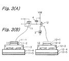
- the second embodiment of the present invention is described in accordance with Fig.3.
- the second embodiment is directed to a thin film transistor (TFT) having an upper gate electrode 11-1(12-1), and a lower gate electrode 11-5(12-5).
- TFT thin film transistor
- Fig.3A is a circuit diagram of one pixcel of an image display system, and Fig.3B shows structure of each TFT.
- the TFT 11 functions as a select FET
- the TFT 12 functions as a bias FET
- the select TFT 11 comprises an upper gate electrode 11-1, an upper gate oxide layer 11-2, an active layer 11-3, a lower gate oxide layer 11-4, and a lower gate electrode 11-5.
- the upper gate oxide layer 11-2 is thinner than the lower gate oxide layer 11-4.
- the select TFT 11 is produced as follows.
- a substrate is patterned with poly-silicon to form a lower gate electrode 11-5, on which a lower gate oxide layer 11-4 is deposited by forming SiO 2 layer by 1000 ⁇ thickness through plasma CVD process with TEOS gas (Tetra-Ethoxy-Silane).
- TEOS gas Tetra-Ethoxy-Silane
- an amorphous silicon layer is deposited through CVD process with SiH 4 gas, and the amorphous silicon layer is solid-developed to provide a poly-silicon layer which functions as an active layer 11-3, on which an upper gate oxide layer 11-2 of SiO 2 layer of 500 ⁇ thickness is formed.
- an upper gate electrode 11-1 of poly-silicon layer is deposited on the upper gate oxide layer 11-2.
- the select TFT 12 comprises, as shown in Fig.3B, an upper gate electrode 12-2, an active layer 12-3, a lower gate oxide layer 12-4, and a lower gate electrode 12-5.
- the upper gate oxide layer 12-2 is thinner than the lower gate oxide layer 12-4, as is the case of the TFT 11.
- the structure of the TFT 12 is the same as that of the TFT 11, except that the TFT 12 has no upper gate electrode 12-1.
- the TFT,s 11 and 12 are produced at the same time.
- the upper gate electrode 12-1 may be removed after both the gate electrodes 11-1 and 12-1 are produced, alternatively, only the upper gate electrode 11-1 is produced but not the upper gate electrode 12-1.
- the bias TFT 12 uses the thick lower gate oxide layer 12-4, and the select TFT 11 uses the thin upper gate oxide layer 11-2, so that the value S of the bias TFT 12 is large, and the value S of the select TFT 11 is smaller than that of the TFT 12. Thus, high quality image display system is obtained.
- the upper gate electrode 11-1 may be connected to the lower gate electrode 11-5. Since the lower gate oxide layer 11-4 is thicker than the upper gate oxide layer 11-2, the control function of the TFT 11 is essentially defined by the upper gate electrode 11-1.
- the third embodiment is described in accordance with Fig.4.
- the TFT of the third embodiment has, as shown in Fig.4, an upper gate electrode 11-1 (13-1), a lower gate electrode 11-5 (13-5), and a lower gate oxide layer (11-4 (13-4) which is made of a thick layer.
- Fig.4A shows a circuit diagram of one pixcel of an image display system
- Fig.4B shows the structure of each TFT.
- the feature of the third embodiment is that both the select TFT and the bias TFT have a thick lower gate oxide layer.
- the select TFT 11 has, as shown in Fig.4B, an upper gate electrode 11-1, an upper gate oxide layer 11-2, an active layer 11-3, a lower gate oxide layer 11-4, and a lower gate electrode 11-5.
- the upper gate oxide layer 11-2 is thinner than the lower gate oxide layer 11-4.
- the bias TFT 13 has, as shown in Fig.4B, an upper gate electrode 13-1, an upper gate oxide layer 13-2, an active layer 13-3, a lower gate oxide layer 13-4, and a lower gate electrode 13-5.
- the upper gate oxide layer 13-2 is thinner than the lower gate oxide layer 13-4.
- the structure of the TFT 11 and the TFT 13 is the same as each other, and those TFT's are produced simultaneously as follows.
- a substrate is patterned with poly-silicon to form lower gate electodes 11-5 and 13-5, on which lower gate oxide layers 11-4 and 13-4 are deposited by forming SiO 2 layer by 1000 A thickness through plasma CVD process with TEOS gas.
- an amorphous silicon layer is deposited through CVD process with SiH 4 gas, and the amorphous silicon layer is solid-phase developed to provide a poly-silicon layer which functions as active layers 11-3 and 13-3, on which upper gate oxide layers 11-2 and 13-2 of SiO 2 of 500 A thickness are formed.
- upper gate electrodes 11-1 and 13-1 of poly-silicon layer are deposited on the upper gate oxide layers.
- the upper gate electrode 11-1 of the TFT 11 is connected to the lower gate electrode 11-5, and those gate electrodes receive the common control voltage.
- the control characteristics of the TFT 11 is essentially defined by the upper gate oxide layer 11-1, but not the lower gate oxide layer 11-4.
- the upper gate electrode 13-1 is coupled with the source electrode and high voltage of the power source Vdd. Since the power source voltage is fixed, the upper gate electrode has no control function. Thus, the control function of the TFT 13 is obtained by the lower gate electrode 13-5.
- the value S of the bias TFT 13 is large since the thick lower gate oxide layer 13-4 is used for the control.
- the value S of the select TFT 11 is small since the thin upper gate oxide layer 11-2 is used for the control. Thus, high quality image display system is obtained.
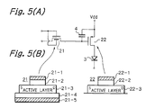
- a select TFT 21 in the fourth embodiment comprises, as shown in Fig.5B, an upper gate electrode 21-1, an upper gate oxide layer 21-2, an active layer 21-3, a lower gate oxide layer 21-4, and a lower gate electrode 21-5.
- the thickness of the upper gate oxide layer 21-2 is larger than the thickness of the lower gate oxide layer 21-4.
- a bias TFT 22 in the fourth embodiment comprises an upper gate electrode 22-1, an upper gate oxide layer 22-2, and an active layer 22-3. No lower gate oxide layer nor lower gate oxide layer is provided in the bias TFT 22 in the fourth embodiment.
- the select TFT 21 is produced as follows. A substrate is patterned with poly-silicon to form a lower gate electrode 21-5, on which a lower gate oxide layer 21-4 is deposited by forming SiO 2 layer by 500 ⁇ thickness through plasma CVD process with TEOS gas. On the lower gate oxide layer 21-4, an amorphous silicon layer is deposited through CVD process with SiH 4 gas, and the amorphous silicon layer is solid-phase developed to provide a poly-silicon layer which functions as an active layer 21-3, on which an upper gate oxide layer 21-2 of SiO 2 layer 1000 ⁇ is formed. Then, an upper gate electrode 21-1 of poly-silicon layer is deposited on the upper gate oxide layer 21-2.
- the active layer 22-3, the gate oxide layer 22-2, and the upper gate electrode 22-1 are produced simultaneously when the active layer 21-3, the upper gate oxide layer 21-2 and the upper gate electrode 21-1 of the TFT 21 are produced, respectively.
- the upper gate electrode 21-1 of the select TFT 21 is coupled with the lower gate electrode 21-5. Since the upper gate oxide layer 21-2 is thicker than the lower gate oxide layer 21-4, the control function of the TFT 21 is defined by the lower gate electrode 21-5.
- the value S of the select TFT 21 is small since the thin lower gate oxide layer 21-4 is used.
- the value S of the bias TFT 22 is large since the thick gate oxide layer 22-2 is used. Thus, high quality image display system is obtained.
- the fifth embodiment is described in accordance with Fig.6.
- Fig.6A is a circuit diagram of one pixcel of an image display system, and Fig.6B shows structure of each TFT.
- the select TFT 21 in Fig.6 comprises an upper electrode 21-1, a thick upper gate oxide layer 21-2, an active layer 21-3, a thin lower gate oxide layer 21-4, and a lower gate electrode 21-5.
- the bias TFT 23 comprises an upper gate electrode 23-1, a thick upper gate oxide layer 23-2, an active layer 23-3, a thin lower gate oxide layer 23-4 and a lower gate electrode 23-5.
- the structure of the TFT 21 is the same as the structure of the TFT 23, and those TFT's are produced simultaneously as follows.
- a substrate is patterned with poly-silicon to form a lower gate electrodes 21-5, on which a lower gate oxide layers 21-4 is deposited by forming SiO 2 layer by 500 ⁇ thickness through plasma CVD process with TEOS gas.
- a lower gate oxide layer 21-4 an amorphous silicon layer is deposited through CVD process with SiH 4 gas, and the amorphous silicon layer is solid-phase developed to provide a poly-silicon layer which functions as an active layer 21-3, on which an upper gate oxide layer 21-2 of SiO 2 layer of 1000 A thickness is formed.
- an upper gate electrode 21-1 of poly-silicon layer is deposited on the upper gate oxide layer 21-2.
- the TFT 23 is produced at the same time as the TFT 21.
- the upper gate electrode 21-1 of the TFT 21 is connected to the lower gate electrode 21-5 of the TFT 21, as shown in Fig.6A. Since the upper gate oxide layer 21-2 is thicker than the lower gate oxide layer 21-4, the control function of the TFT 21 is defined by the lower gate oxide layer 21-4.
- the lower gate electrode 23-5 of the bias TFT 23 is connected to the source of the TFT 23, and the fixed power source voltage Vdd. As the power source voltage Vdd is fixed, the lower gate electrode 23-5 has no control function. Thus, the control function of the light control TFT 23 is determined by the upper gate electrode 23-1.
- the value S of the select TFT 21 is small since it is defined by the thin lower gate oxide layer 21-4, and the value S of the bias TFT 23 is large since it is defined by the thick upper gate oxide layer 23-2. Thus, high quality image display system is obtained.
- the sixth embodiment of the present invention is described in accordance with Fig.7.
- the value S of a TFT is determined by designing dielectric constant of a gate oxide layer.
- a select TFT 51 comprises a gate electrode 51-1, a gate oxide layer 51-2, and an active layer 51-3
- a bias TFT 52 comprises a gate electrode 52-1, a gate oxide layer 52-2 and an active layer 52-3.
- the dielectric constant ⁇ 51 of the gate oxide layer 51-2 is larger than the dielectric constant ⁇ 52 of the gate oxide layer 52-2, so that ⁇ 51 > ⁇ 52 . Therefore, the value S of the TFT 51 is smaller than the value S of the TFT 52.
- the producing steps for providing the relations ⁇ 51 > ⁇ 52 is as follows. After the active layers 51-3 and 52-3 are produced on a substrate, a gate oxide layer 51-2 is first produced through plasma CVD process with SiH 4 , N 2 O and ammonia gas. Then, a gate oxide layer 52-2 is produced through plasma CVD process with less ammonia gas. The amount of ammonia gas when the gate oxide layer 51-2 is produced is larger than that when the gate oxide layer 52-2 is produced. Then, the gate electrodes 51-1 and 52-1 are produced on the gate oxide layers 51-2 and 52-2, respectively.
- the dielectric constant ⁇ 51 of the gate oxide layer 51-2 is larger than the dielectric constant ⁇ 52 of the gate oxide layer 52-2.
- the value S of a bias TFT 52 is larger than the value S of a select TFT 51, and high quality image display system is obtained.
- the seventh embodiment of the present invention is described in accordance with Fig.8.
- the seventh embodiment has TFT's 61 and 62, each comprising an upper gate electrode 61-1 (62-1), an upper gate oxide layer 61-2 (62-2) with small dielectric constant, an active layer 61-3 (62-3), a lower gate oxide layer 61-4 (62-4) with larger dielectric constant than that of an upper gate oxide layer, and a lower gate electrode 61-5 (62-5).
- the producing steps for a TFT are as follows.
- a substrate is patterned with poly-silicon to form lower gate electrodes 61-5, and 62-5, on which lower gate oxide layers 61-4 and 62-4 are deposited through plasma CVD process with SiH 4 , N 2 O and ammonia gas.
- an amorphous silicon layer is deposited through CVD process with SiH 4 gas, and the amorphous silicon layer is solid-phase developed to provide a poly-silicon layer which functions as active layers 61-3 and 62-3, on which upper gate oxide layers 61-2 and 62-2 are formed through CVD process with SiH 4 , N 2 O and ammonia gas, and upper gate electrodes 61-1 and 62-2 are formed on the upper gate oxide layers.
- the amount of ammonia gas when the lower gate oxide layers are produced is larger than the amount of ammonia gas when the lower gate oxide layers are produced.
- the dielectric constant ⁇ 4 of the lower gate oxide layers is larger than the dielectric constant ⁇ 2 of the upper gate oxide layers ( ⁇ 4 > ⁇ 2 ).
- the upper gate electrode 61-1 of the select TFT 61 is connected to a fixed voltage so that the upper gate electrode 61-1 does not function as a control gate, and the lower gate electrode 61-4 operates as a control gate.
- the lower gate electrode 62-4 of the bias TFT 62 is fixed to the source voltage Vdd so that the lower gate electrode does not function as a control gate, and the upper gate electrode 62-2 operates as a control gate.
- the control is carried out by the lower gate oxide layer 61-4 which has high dielectric constant
- the bias TFT 62 the control is carried out by the upper gate electrode 62-2 which has low dielectric constant.
- the value S of a bias TFT 62 is high, and the value S of a select TFT 61 is lower than that of a bias TFT 62, and high quality image display system is obtained.
- Each TFT in the eighth embodiment comprises, as shown in Fig.8, an upper gate electrode, an upper gate oxide layer, an active layer, a lower gate oxide layer and a lower gate electrode.
- the dielectric constant of an upper gate oxide layer is larger than the dielectric constant of a lower gate oxide layer.
- An upper gate electrode of a select TFT is used as a control gate, and an upper gate electrode of a select TFT is connected to a fixed voltage so that it does not function as a control gate.
- a bias TFT a lower gate electrode is used as a control gate, and an upper gate electrode is fixed to a source voltage.
- the value S of a select TFT is kept small, and the value S of only a bias TFT is large.
- high quality image display system is provided.
- modifying the value S are to modify the thickness of a gate oxide layer, and to modify the dielectric constant of a gate oxide layer. Those modification means may be used not only by using only one of them, but also with combination.
- the present invention provides high quality image display system by using a bias FET with the larger value S than that of a select FET.
Landscapes
- Engineering & Computer Science (AREA)
- Physics & Mathematics (AREA)
- Computer Hardware Design (AREA)
- General Physics & Mathematics (AREA)
- Theoretical Computer Science (AREA)
- Geometry (AREA)
- Microelectronics & Electronic Packaging (AREA)
- Control Of Indicators Other Than Cathode Ray Tubes (AREA)
- Electroluminescent Light Sources (AREA)
- Thin Film Transistor (AREA)
- Control Of El Displays (AREA)
- Devices For Indicating Variable Information By Combining Individual Elements (AREA)
Applications Claiming Priority (2)
| Application Number | Priority Date | Filing Date | Title |
|---|---|---|---|
| JP12659197A JP3530341B2 (ja) | 1997-05-16 | 1997-05-16 | 画像表示装置 |
| JP126591/97 | 1997-05-16 |
Publications (2)
| Publication Number | Publication Date |
|---|---|
| EP0878789A2 true EP0878789A2 (fr) | 1998-11-18 |
| EP0878789A3 EP0878789A3 (fr) | 1999-03-17 |
Family
ID=14938983
Family Applications (1)
| Application Number | Title | Priority Date | Filing Date |
|---|---|---|---|
| EP98410051A Ceased EP0878789A3 (fr) | 1997-05-16 | 1998-05-13 | Dispositif d'affichage |
Country Status (3)
| Country | Link |
|---|---|
| US (1) | US6100860A (fr) |
| EP (1) | EP0878789A3 (fr) |
| JP (1) | JP3530341B2 (fr) |
Cited By (13)
| Publication number | Priority date | Publication date | Assignee | Title |
|---|---|---|---|---|
| EP1191512A3 (fr) * | 2000-09-20 | 2002-08-21 | Seiko Epson Corporation | Circuit de commande pour un dispositif d'affichage à matrice active, méthode de commande d'un équipement et d'un appareil électronique et appareil électronique |
| WO2002025366A3 (fr) * | 2000-09-19 | 2002-08-29 | Display Res Labroatories Inc | Transistors a couches minces pouvant etre utilises pour la confection d'ecrans plats |
| US6864508B2 (en) | 2001-07-17 | 2005-03-08 | Semiconductor Energy Laboratory Co., Ltd. | Light emitting device |
| US7109073B2 (en) | 2001-08-17 | 2006-09-19 | Semiconductor Energy Laboratory Co., Ltd. | Method for fabricating semiconductor device |
| US7112517B2 (en) | 2001-09-10 | 2006-09-26 | Semiconductor Energy Laboratory Co., Ltd. | Laser treatment device, laser treatment method, and semiconductor device fabrication method |
| US7317205B2 (en) | 2001-09-10 | 2008-01-08 | Semiconductor Energy Laboratory Co., Ltd. | Light emitting device and method of manufacturing a semiconductor device |
| US7422987B2 (en) | 2001-08-30 | 2008-09-09 | Semiconductor Energy Laboratory Co., Ltd. | Method for manufacturing semiconductor device |
| EP1096571A3 (fr) * | 1999-10-29 | 2009-11-18 | Sel Semiconductor Energy Laboratory Co., Ltd. | Dispositif électronique |
| US7982222B2 (en) | 1999-06-23 | 2011-07-19 | Semiconductor Energy Laboratory Co., Ltd. | EL display device and electronic device |
| CN101572057B (zh) * | 2008-04-30 | 2012-01-25 | 索尼株式会社 | 显示装置 |
| US8933624B2 (en) | 1999-10-26 | 2015-01-13 | Semiconductor Energy Laboratory Co., Ltd. | Light emitting device |
| US9837451B2 (en) | 1999-04-27 | 2017-12-05 | Semiconductor Energy Laboratory Co., Ltd. | Electronic device and electronic apparatus |
| US9910334B2 (en) | 1999-02-23 | 2018-03-06 | Semiconductor Energy Laboratory Co., Ltd. | Semiconductor device and fabrication method thereof |
Families Citing this family (20)
| Publication number | Priority date | Publication date | Assignee | Title |
|---|---|---|---|---|
| FR2772501B1 (fr) * | 1997-12-15 | 2000-01-21 | Thomson Lcd | Dispositif de commande matriciel |
| JP2000068065A (ja) | 1998-08-13 | 2000-03-03 | Tdk Corp | 有機el素子 |
| JP3879281B2 (ja) * | 1998-11-06 | 2007-02-07 | カシオ計算機株式会社 | 表示装置及び表示装置の駆動方法 |
| JP4423701B2 (ja) | 1999-06-07 | 2010-03-03 | Tdk株式会社 | 有機el表示装置 |
| TW522453B (en) * | 1999-09-17 | 2003-03-01 | Semiconductor Energy Lab | Display device |
| TW587239B (en) * | 1999-11-30 | 2004-05-11 | Semiconductor Energy Lab | Electric device |
| TW493152B (en) * | 1999-12-24 | 2002-07-01 | Semiconductor Energy Lab | Electronic device |
| WO2001054107A1 (fr) * | 2000-01-21 | 2001-07-26 | Emagin Corporation | Circuit d'excitation de pixels a echelle de gris pour affichage electronique et son procede d'exploitation |
| JP4014831B2 (ja) * | 2000-09-04 | 2007-11-28 | 株式会社半導体エネルギー研究所 | El表示装置及びその駆動方法 |
| JP3638926B2 (ja) * | 2001-09-10 | 2005-04-13 | 株式会社半導体エネルギー研究所 | 発光装置及び半導体装置の作製方法 |
| KR100826009B1 (ko) * | 2001-11-03 | 2008-04-29 | 엘지디스플레이 주식회사 | 일렉트로 루미네센스 패널 |
| US7109952B2 (en) * | 2002-06-11 | 2006-09-19 | Samsung Sdi Co., Ltd. | Light emitting display, light emitting display panel, and driving method thereof |
| JP2005099715A (ja) * | 2003-08-29 | 2005-04-14 | Seiko Epson Corp | 電子回路の駆動方法、電子回路、電子装置、電気光学装置、電子機器および電子装置の駆動方法 |
| JP2005174960A (ja) * | 2003-12-05 | 2005-06-30 | National Institute Of Advanced Industrial & Technology | 二重ゲート電界効果トランジスタ |
| US7317434B2 (en) * | 2004-12-03 | 2008-01-08 | Dupont Displays, Inc. | Circuits including switches for electronic devices and methods of using the electronic devices |
| JP4748456B2 (ja) * | 2006-09-26 | 2011-08-17 | カシオ計算機株式会社 | 画素駆動回路及び画像表示装置 |
| JP2009157156A (ja) * | 2007-12-27 | 2009-07-16 | Sony Corp | 画素回路および表示装置 |
| JP2010039118A (ja) | 2008-08-04 | 2010-02-18 | Sony Corp | 表示装置及び電子機器 |
| JP4905442B2 (ja) * | 2008-12-05 | 2012-03-28 | ソニー株式会社 | 半導体装置およびその製造方法 |
| CN105206224B (zh) * | 2015-09-24 | 2018-03-20 | 北京大学深圳研究生院 | 一种具有反馈通道的显示系统 |
Citations (1)
| Publication number | Priority date | Publication date | Assignee | Title |
|---|---|---|---|---|
| US5482878A (en) * | 1994-04-04 | 1996-01-09 | Motorola, Inc. | Method for fabricating insulated gate field effect transistor having subthreshold swing |
Family Cites Families (8)
| Publication number | Priority date | Publication date | Assignee | Title |
|---|---|---|---|---|
| US4237456A (en) * | 1976-07-30 | 1980-12-02 | Sharp Kabushiki Kaisha | Drive system for a thin-film EL display panel |
| US4406997A (en) * | 1981-09-30 | 1983-09-27 | International Business Machines Corporation | Method and means for minimizing the effect of short circuits in flat panel displays |
| JPS59119390A (ja) * | 1982-12-25 | 1984-07-10 | 株式会社東芝 | 薄膜トランジスタ回路 |
| JP2821347B2 (ja) * | 1993-10-12 | 1998-11-05 | 日本電気株式会社 | 電流制御型発光素子アレイ |
| US5550066A (en) * | 1994-12-14 | 1996-08-27 | Eastman Kodak Company | Method of fabricating a TFT-EL pixel |
| JPH08241057A (ja) * | 1995-03-03 | 1996-09-17 | Tdk Corp | 画像表示装置 |
| JPH09101506A (ja) * | 1995-07-31 | 1997-04-15 | Victor Co Of Japan Ltd | 液晶表示装置 |
| US5748160A (en) * | 1995-08-21 | 1998-05-05 | Mororola, Inc. | Active driven LED matrices |
-
1997
- 1997-05-16 JP JP12659197A patent/JP3530341B2/ja not_active Expired - Fee Related
-
1998
- 1998-05-04 US US09/071,161 patent/US6100860A/en not_active Expired - Lifetime
- 1998-05-13 EP EP98410051A patent/EP0878789A3/fr not_active Ceased
Patent Citations (1)
| Publication number | Priority date | Publication date | Assignee | Title |
|---|---|---|---|---|
| US5482878A (en) * | 1994-04-04 | 1996-01-09 | Motorola, Inc. | Method for fabricating insulated gate field effect transistor having subthreshold swing |
Non-Patent Citations (1)
| Title |
|---|
| ISABELLE FERAIN ET AL: "Multigate transistors as the future of classical metal-oxide-semiconductor field-effect transistors", NATURE, vol. 479, no. 7373, 16 November 2011 (2011-11-16), pages 310 - 316, XP055169493, ISSN: 0028-0836, DOI: 10.1038/nature10676 * |
Cited By (23)
| Publication number | Priority date | Publication date | Assignee | Title |
|---|---|---|---|---|
| US9910334B2 (en) | 1999-02-23 | 2018-03-06 | Semiconductor Energy Laboratory Co., Ltd. | Semiconductor device and fabrication method thereof |
| US9837451B2 (en) | 1999-04-27 | 2017-12-05 | Semiconductor Energy Laboratory Co., Ltd. | Electronic device and electronic apparatus |
| US7982222B2 (en) | 1999-06-23 | 2011-07-19 | Semiconductor Energy Laboratory Co., Ltd. | EL display device and electronic device |
| US9391132B2 (en) | 1999-10-26 | 2016-07-12 | Semiconductor Energy Laboratory Co., Ltd. | Light emitting device |
| US8933624B2 (en) | 1999-10-26 | 2015-01-13 | Semiconductor Energy Laboratory Co., Ltd. | Light emitting device |
| EP1096571A3 (fr) * | 1999-10-29 | 2009-11-18 | Sel Semiconductor Energy Laboratory Co., Ltd. | Dispositif électronique |
| US8648345B2 (en) | 1999-10-29 | 2014-02-11 | Semiconductor Energy Laboratory Co., Ltd. | Electronic device |
| US8017945B2 (en) | 1999-10-29 | 2011-09-13 | Semiconductor Energy Laboratory Co., Ltd. | Display device using light-emitting element |
| WO2002025366A3 (fr) * | 2000-09-19 | 2002-08-29 | Display Res Labroatories Inc | Transistors a couches minces pouvant etre utilises pour la confection d'ecrans plats |
| US7091939B2 (en) | 2000-09-20 | 2006-08-15 | Seiko Epson Corporation | System and methods for providing a driving circuit for active matrix type displays |
| EP1191512A3 (fr) * | 2000-09-20 | 2002-08-21 | Seiko Epson Corporation | Circuit de commande pour un dispositif d'affichage à matrice active, méthode de commande d'un équipement et d'un appareil électronique et appareil électronique |
| US6750833B2 (en) | 2000-09-20 | 2004-06-15 | Seiko Epson Corporation | System and methods for providing a driving circuit for active matrix type displays |
| US7485896B2 (en) | 2001-07-17 | 2009-02-03 | Semiconductor Energy Laboratory Co., Ltd. | Light emitting device |
| US7265390B2 (en) | 2001-07-17 | 2007-09-04 | Semiconductor Energy Laboratory Co., Ltd. | Light emitting device |
| US6864508B2 (en) | 2001-07-17 | 2005-03-08 | Semiconductor Energy Laboratory Co., Ltd. | Light emitting device |
| US6952023B2 (en) | 2001-07-17 | 2005-10-04 | Semiconductor Energy Laboratory Co., Ltd. | Light emitting device |
| US7393729B2 (en) | 2001-08-17 | 2008-07-01 | Semiconductor Energy Laboratory Co., Ltd. | Method for fabricating semiconductor device |
| US7109073B2 (en) | 2001-08-17 | 2006-09-19 | Semiconductor Energy Laboratory Co., Ltd. | Method for fabricating semiconductor device |
| US7422987B2 (en) | 2001-08-30 | 2008-09-09 | Semiconductor Energy Laboratory Co., Ltd. | Method for manufacturing semiconductor device |
| US7317205B2 (en) | 2001-09-10 | 2008-01-08 | Semiconductor Energy Laboratory Co., Ltd. | Light emitting device and method of manufacturing a semiconductor device |
| US7112517B2 (en) | 2001-09-10 | 2006-09-26 | Semiconductor Energy Laboratory Co., Ltd. | Laser treatment device, laser treatment method, and semiconductor device fabrication method |
| US7682949B2 (en) | 2001-09-10 | 2010-03-23 | Semiconductor Energy Laboratory Co., Ltd. | Laser treatment device, laser treatment method, and semiconductor device fabrication method |
| CN101572057B (zh) * | 2008-04-30 | 2012-01-25 | 索尼株式会社 | 显示装置 |
Also Published As
| Publication number | Publication date |
|---|---|
| JPH10319907A (ja) | 1998-12-04 |
| EP0878789A3 (fr) | 1999-03-17 |
| JP3530341B2 (ja) | 2004-05-24 |
| US6100860A (en) | 2000-08-08 |
Similar Documents
| Publication | Publication Date | Title |
|---|---|---|
| US6100860A (en) | Image display device | |
| JP4170384B2 (ja) | 自発光型表示装置 | |
| US7804469B2 (en) | Display apparatus and driving method for display apparatus | |
| JP5028723B2 (ja) | 薄膜トランジスタ、該薄膜トランジスタの製造方法、該薄膜トランジスタを含むアレイ基板、表示装置および該表示装置の駆動方式 | |
| EP1033765B1 (fr) | Elément de commutation et dispositif d'affichage electroluminescent | |
| CN100371974C (zh) | 显示驱动器 | |
| US6084579A (en) | Display apparatus using electroluminescence elements | |
| US7928932B2 (en) | Display element drive circuit and display apparatus | |
| US11527595B2 (en) | Light emitting apparatus, imaging apparatus, electronic apparatus, illumination apparatus, and mobile apparatus | |
| CA2496642A1 (fr) | Methode d'attaque a courte duree de stabilisation pour afficheurs a diodes organiques electroluminescentes (oled) programmes par courant | |
| JP2006502433A (ja) | エレクトロルミネッセンス表示装置 | |
| JP2002517806A (ja) | アクティブマトリックス電界発光表示装置 | |
| EP1741084A2 (fr) | Ecran emissif ameliore a matrice active stabilisee | |
| KR20200008049A (ko) | 발광 장치 | |
| CN101196663A (zh) | 液晶显示设备及其驱动方法 | |
| JP2003518772A (ja) | トランジスタ閾値電圧の変化への敏感度を低減した薄膜トランジスタ回路 | |
| JP2006525539A (ja) | 閾値電圧のドリフト補償を有するアクティブマトリクスoled表示装置 | |
| CN101385064B (zh) | 大面积薄膜电路 | |
| TW200303503A (en) | Light-emitting device | |
| CN1910642A (zh) | 具有有源矩阵的电致发光显示设备 | |
| JPH0916123A (ja) | 画像表示装置 | |
| WO2002071379A2 (fr) | Circuit de commande de type a courant pour afficheur a diodes lumineuses organiques | |
| CN100421142C (zh) | 电致发光显示器件及其驱动方法 | |
| JP2007524118A (ja) | アクティブマトリクス表示装置 | |
| US20100201717A1 (en) | Display device and driving method thereof |
Legal Events
| Date | Code | Title | Description |
|---|---|---|---|
| PUAI | Public reference made under article 153(3) epc to a published international application that has entered the european phase |
Free format text: ORIGINAL CODE: 0009012 |
|
| AK | Designated contracting states |
Kind code of ref document: A2 Designated state(s): DE FR GB NL |
|
| AX | Request for extension of the european patent |
Free format text: AL;LT;LV;MK;RO;SI |
|
| PUAL | Search report despatched |
Free format text: ORIGINAL CODE: 0009013 |
|
| AK | Designated contracting states |
Kind code of ref document: A3 Designated state(s): AT BE CH CY DE DK ES FI FR GB GR IE IT LI LU MC NL PT SE |
|
| AX | Request for extension of the european patent |
Free format text: AL;LT;LV;MK;RO;SI |
|
| 17P | Request for examination filed |
Effective date: 19990814 |
|
| AKX | Designation fees paid |
Free format text: DE FR GB NL |
|
| 17Q | First examination report despatched |
Effective date: 20071002 |
|
| RAP1 | Party data changed (applicant data changed or rights of an application transferred) |
Owner name: SEMICONDUCTOR ENERGY LABORATORY CO., LTD. Owner name: TDK CORPORATION |
|
| STAA | Information on the status of an ep patent application or granted ep patent |
Free format text: STATUS: THE APPLICATION HAS BEEN REFUSED |
|
| 18R | Application refused |
Effective date: 20151201 |