EP0878844A2 - Dispositif à hautes-fréquences comportant un substrat à faibles pertes - Google Patents
Dispositif à hautes-fréquences comportant un substrat à faibles pertes Download PDFInfo
- Publication number
- EP0878844A2 EP0878844A2 EP98302203A EP98302203A EP0878844A2 EP 0878844 A2 EP0878844 A2 EP 0878844A2 EP 98302203 A EP98302203 A EP 98302203A EP 98302203 A EP98302203 A EP 98302203A EP 0878844 A2 EP0878844 A2 EP 0878844A2
- Authority
- EP
- European Patent Office
- Prior art keywords
- substrate
- single crystal
- ohm
- polycrystalline
- inductor
- Prior art date
- Legal status (The legal status is an assumption and is not a legal conclusion. Google has not performed a legal analysis and makes no representation as to the accuracy of the status listed.)
- Ceased
Links
Images


Classifications
-
- H—ELECTRICITY
- H10—SEMICONDUCTOR DEVICES; ELECTRIC SOLID-STATE DEVICES NOT OTHERWISE PROVIDED FOR
- H10W—GENERIC PACKAGES, INTERCONNECTIONS, CONNECTORS OR OTHER CONSTRUCTIONAL DETAILS OF DEVICES COVERED BY CLASS H10
- H10W70/00—Package substrates; Interposers; Redistribution layers [RDL]
- H10W70/60—Insulating or insulated package substrates; Interposers; Redistribution layers
- H10W70/67—Insulating or insulated package substrates; Interposers; Redistribution layers characterised by their insulating layers or insulating parts
- H10W70/69—Insulating materials thereof
- H10W70/698—Semiconductor materials that are electrically insulating, e.g. undoped silicon
Definitions
- This invention pertains to high frequency electronic apparatus, exemplarily a RF, UHF or micro-wave transceiver, that comprises a low loss substrate.
- the apparatus also comprises a transmission line and/or a planar inductor on the substrate.
- High frequency apparatus of the type of concern herein generally requires, in addition to active elements such as transistors, passive elements such as resistors, capacitors and inductors, as well as transmission lines. Whereas resistors and capacitors are readily compatible with conventional IC technology, prior art inductors generally are not. Furthermore, prior art inductors generally require substantial "real estate" on a chip, and typically have relatively low quality factor (Q).
- Q quality factor
- inductors for use in or with integrated circuits are formed on a resistive substrate, exemplarily a single crystal silicon (Si) substrate, a glass substrate or a co-fired ceramic substrate. All of these have shortcomings, however.
- Single crystal Si substrates have high thermal conductivity, which facilitates heat removal. Si single crystal substrates also facilitate flip-chip, fine line thin film interconnections, are readily compatible with integrated resistors and capacitors, and to date can provide maximum miniaturization to provide the best electrical environment. Inductors on single crystal Si substrates can be accurately modeled and simulated, thereby facilitating circuit design and development.
- the resistivity of commercially available single crystal Si substrates typically is only about 2000 ohms ⁇ cm or less, with the cost of higher resistivity single crystal Si wafers, if at all available, likely increasing steeply with increasing resistivity.
- typical obtainable values of Q are 10-20, depending on the value of inductance and the geometry of the inductor.
- Glass substrates are good insulators and therefore can yield high Q inductors.
- glass substrates are poor heat conductors, and also have other disadvantages. Due to the relatively fragile nature of glass and the thermal expansion mismatch between the glass substrate and other materials (e.g., Si), cracks and breaks in the substrate are quite frequent, resulting in low yield and potentially, low reliability.
- materials e.g., Si
- Co-fired ceramic substrates have high resistivity and thus also can yield high Q inductors.
- co-fired ceramic substrates typically are also relatively poor heat conductors, and require the use of screen printing to define the conductor structure, and thus inherently have relatively large feature size.
- typically several layers of ceramic are required in order to achieve the same level of integration as in the case of thin film technology.
- Such substrates typically are relatively expensive, and it is typically difficult to model circuits that involve such substrates.
- a low cost substrate that substantially retains the many advantages of single crystal Si and has resistivity higher than that of conventional single crystal Si would clearly be highly desirable.
- This application discloses such a substrate, and circuitry formed on the substrate.
- the invention is defined by the claims.
- the invention is embodied in an article (e.g., a high frequency transceiver, a wireless telephone handset, a "personal communicator", or a communication system that comprises such transceivers, handsets or personal communicators) that comprises a low cost, relatively low loss (high resistivity) substrate, exemplarily with a transmission line and/or an inductive circuit element disposed on the substrate.
- a high frequency transceiver e.g., a high frequency transceiver, a wireless telephone handset, a "personal communicator”, or a communication system that comprises such transceivers, handsets or personal communicators
- a low cost, relatively low loss (high resistivity) substrate exemplarily with a transmission line and/or an inductive circuit element disposed on the substrate.
- the article comprises a silicon substrate.
- an inductive circuit element e.g., a spiral coil
- a quality factor Q of the inductive circuit element is a function of the resistivity of the silicon body.
- the inductive circuit element (to be referred to as the "inductor") is disposed on the silicon substrate, with a dielectric layer (typically SiO 2 ) between the silicon substrate and the inductor.
- the Q of the inductor is a function of the resistivity of the silicon body if the electromagnetic field of the inductor penetrates into the silicon body.
- the silicon body is a polycrystalline silicon body havingresistivity greater than about 2000 ohm ⁇ cm, desirably as much as 10 4 ohm ⁇ cm or even more.
- the high frequency apparatus can have improved performance (e.g., increased Q of an inductor and/or lower loss transmission lines), typically at reduced cost, as compared to analogous prior art apparatus that comprises a conventional single crystal Si substrate.
- polycrystalline silicon we mean herein silicon of grain size small enough to provide sufficient grain boundary scattering to give resistivity greater than 2000 ohm ⁇ cm. Exemplarily the average grain size is less than 10 ⁇ m.
- polycrystalline Si is available at relatively low cost, since such material is an intermediate product in the manufacture of single crystal Si for electronic device manufacture.
- polycrystalline Si suitable for practice of the invention can be obtained from Advanced Silicon Materials, Inc., of Moses Lake, Washington.
- the polycrystalline material typically is in the form of aboule, similar to conventional single crystal material, with the cost of a boule of polycrystalline material exemplarily being less than 50% of the cost of a similar boule for conventional single crystal silicon.
- the cost of sectioning into wafers and polishing of the wafers can be expected to be substantially the same for both types of silicon, at least after the demand for polycrystalline wafers has increased due to widespread practice of the instant invention.
- boules of polycrystalline silicon frequently are in a state of stress, and that it is typically advantageous to relieve the stresses by an appropriate heat treatment (e.g., 12 hours at 1000°C) before sectioning of the boules.
- Such a treatment will typically add little to the cost of polycrystalline Si wafers, and is not expected to substantially affect the cost advantage of polycrystalline Si wafers over conventional single crystal Si wafers.
- Use of a polycrystalline Si substrate not only offers an economic advantage over conventional single crystal Si substrates but typically also has technological advantages, e.g., attainment of inductors having higher Q, and lower loss transmission lines.
- Polycrystalline Si substrates will typically find use in high frequency, (e.g., RF, UHF and microwave frequency, typically ⁇ 800 MHz) applications. It is thus important that the material exhibits high resistivity at high frequencies. This was verified as follows.
- Co-planar waveguide (CPW) transmission lines were fabricated by conventional means on a polycrystalline Si substrate, substantially as shown in FIG. 1 in top view.
- the substrate was commercially available polycrystalline silicon (675 ⁇ m thick).
- the transmission lines 10 were 2 mm, 6 mm and 16 mm long, with central conductor 11 being 50 ⁇ m wide, with spacing between central conductor and ground electrodes 12 being 39 ⁇ m.
- Ground electrodes and central conductor were 3 ⁇ m thick Al.
- the transmission lines were characterized by measuring the scattering parameters (S-matrix) over the frequency range 2 GHz - 18 GHz. Such measurements are conventional and can be carried out with commercially available apparatus, e.g., a Hewlett-Packard 8510 Network Analyzer.
- the S 21 matrix element includes the transmission line loss and the mismatch loss.
- the latter can be eliminated from the measured S 21 by comparing transmission lines of different lengths, yielding the value of the transmission line loss of a given line.
- the transmission line loss indicates how well the transmission line performs at high frequency. The smaller the loss, the better the performance.
- the measured insertion losses at 18 GHz were 0.6 dB, 0.7 dB and 1.0 dB, respectively for the 2 mm, 6 mm and 16 mm long lines, yielding values of 0.25 dB/cm, 0.3 dB/cm and 0.29 dB/cm. From these and other results we concluded that the polycrystalline Si substrate had excellent electrical performance, comparable to that of a semi-insulating GaAs substrate, but with much better heat dissipation performance and mechanical strength than GaAs.
- FIG. 2 shows exemplary results of S 21 vs. frequency for the above-described CPW transmission lines on polycrystalline Si. .
- the insertion loss is relatively low and substantially frequency-independent over the range 2-18 GHz.
- FIGs. 3 and 4 were made by a conventional technique, using a Hewlett-Packard 4291A Impedance Analyzer.
- FIG. 3 shows the dielectric constant as a function of frequency for 2 k ⁇ . cm single crystal Si (curve 31), and polycrystalline Si (curve 32). As can be seen, the two materials have substantially identical dielectric constant.
- FIG. 4 shows loss tangent as a function of frequency, for 2k ⁇ . cm single crystal Si (curve 41) and polycrystalline Si (curve 42).
- the polysilicon ⁇ 10k ⁇ . cm
- the loss tangent of the former was substantially the same as that of glass.
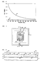
- FIG. 5 shows an exemplary (500 ⁇ m x 500 ⁇ m) spiral inductor on a polycrystalline substrate in top view
- FIG. 6 schematically depicts an inductor, similar to that of FIG. 4, in cross section, substantially along section line A-A'-A" of FIG. 5.
- FIG. 6 shows only two inductor turns.
- numeral 71 refers to the polycrystalline Si substrate (675 ⁇ m thick, about 10 4 ohm ⁇ cm resistivity), 72 to a 1 ⁇ m SiO 2 layer, and 73 to the Al conductor that connects via 762 and 761.
- Numerals 74 and 75 refer each to a 5 ⁇ m polyimide layer, and numerals 781-784 refer to inductor lines (exemplarily Al of 15 ⁇ m x 3 ⁇ m cross section, with 15 ⁇ m spacing between adjacent lines).
- Numeral 77 refers to the ground line contact, and 79 refers to the second inductor terminal.
- Polyimide layer 74 is patterned to provide via holes, and layer 75 is patterned to facilitate electrical contact to the inductor, as indicated schematically by contacts 791 and 792.
- Numeral 793 refers to the short conductor line that connects the inductor to terminal 792.
- FIG. 5 Corresponding features in FIG. 5 are designated by the same numerals as in FIG. 6.
- Numeral 51 refers to the ground ring, and numerals 521 and 522 refer to probe contacts.
- FIG. 7 shows computed curves of quality factor Q vs. frequency, for inductors of geometry as shown in FIGs. 5 and 6, except that the inductor line thickness was assumed to be 6 ⁇ m, in order to reduce metal loss.
- Curves 81-84 of FIG. 7 pertain to inductors on substrates of resistivity 20 ohm ⁇ cm, 2000 ohm ⁇ cm, 10,000 ohm ⁇ cm and 20,000 ohm ⁇ cm, respectively.
- a large improvement in Q results from going from a 20 ohm ⁇ cm substrate to a 2000 ohm ⁇ cm substrate, and a significant improvement results for going from the latter to a 10,000 ohm ⁇ cm substrate.
- the geometry considered very little is gained by going from 10,000 ohm ⁇ cm to 20,000 ohm ⁇ cm, due to metal loss.
- FIG. 8 schematically depicts a relevant portion of exemplary high frequency apparatus 80 according to the invention, wherein numeral 81 refers to a polycrystalline Si substrate according to the invention.
- numeral 82 refers to a conventional IC chip, solder-bonded to the substrate, and numeral 83 refers to a SiO 2 layer thereon.
- Numerals 84-86 respectively refer to a resistor, capacitor and inductor, disposed on the SiO 2 layer.
- Numeral 841 refers to moderately conductive material (e.g.,TaSi) connecting Al vias 842 and 843.
- Numerals 871-874 refer to portions of a patterned dielectric layer (exemplarily Si 3 N 4 ), with portion 873 serving as the dielectric layer of capacitor 85.
- Numeral 851 refers to moderately conductive material (e.g., TaSi) that forms one plate of capacitor 85
- numeral 852 refers to the other plate (typically Al) of the capacitor
- numeral 853 refers to a Al via that provides contact to capacitor plate 851.
- Numerals 861-864 refer to windings of inductor 86. Means for contacting the inductor windings are conventional and are not shown.
- Numerals 88 and 89 refer to polyimide layers
- numeral 90 refers to a solder ball that electrically connects chip 82 to conductor 91 on the substrate.
- Conductors 92-94 are disposed on two different metallization layers and are conventional, as is via metallization 95.
Landscapes
- Semiconductor Integrated Circuits (AREA)
- Crystals, And After-Treatments Of Crystals (AREA)
- Coils Or Transformers For Communication (AREA)
Applications Claiming Priority (2)
| Application Number | Priority Date | Filing Date | Title |
|---|---|---|---|
| US83255097A | 1997-04-03 | 1997-04-03 | |
| US832550 | 1997-04-03 |
Publications (2)
| Publication Number | Publication Date |
|---|---|
| EP0878844A2 true EP0878844A2 (fr) | 1998-11-18 |
| EP0878844A3 EP0878844A3 (fr) | 1998-11-25 |
Family
ID=25261981
Family Applications (1)
| Application Number | Title | Priority Date | Filing Date |
|---|---|---|---|
| EP98302203A Ceased EP0878844A3 (fr) | 1997-04-03 | 1998-03-24 | Dispositif à hautes-fréquences comportant un substrat à faibles pertes |
Country Status (4)
| Country | Link |
|---|---|
| EP (1) | EP0878844A3 (fr) |
| JP (1) | JPH10284694A (fr) |
| KR (1) | KR19980081048A (fr) |
| TW (1) | TW392392B (fr) |
Cited By (5)
| Publication number | Priority date | Publication date | Assignee | Title |
|---|---|---|---|---|
| WO2000048253A1 (fr) * | 1999-02-15 | 2000-08-17 | Telefonaktiebolaget Lm Ericsson | Ci muni d'une bobine d'induction empechant le verrouillage et procede de fabrication associe |
| EP0969500A3 (fr) * | 1998-06-10 | 2000-10-25 | Lucent Technologies Inc. | Circuits intégrés de silicium monocristallin sur silicium polycristallin |
| EP1592047A2 (fr) | 2004-04-29 | 2005-11-02 | Sychip Inc. | Composant intégré passif et son procédé de fabrication |
| US7405643B2 (en) | 2005-01-03 | 2008-07-29 | Samsung Electronics Co., Ltd. | Inductor and method of forming the same |
| EP1835536A3 (fr) * | 2006-03-17 | 2010-07-14 | Sychip Inc. | Substrat pour des dispositifs passifs intégrés |
Families Citing this family (5)
| Publication number | Priority date | Publication date | Assignee | Title |
|---|---|---|---|---|
| JP4005762B2 (ja) * | 1999-06-30 | 2007-11-14 | 株式会社東芝 | 集積回路装置及びその製造方法 |
| JPWO2003007379A1 (ja) | 2001-07-12 | 2004-11-04 | 株式会社日立製作所 | 電子回路部品 |
| TW560017B (en) | 2001-07-12 | 2003-11-01 | Hitachi Ltd | Semiconductor connection substrate |
| US7382056B2 (en) * | 2004-04-29 | 2008-06-03 | Sychip Inc. | Integrated passive devices |
| ATE388520T1 (de) | 2004-05-06 | 2008-03-15 | Nxp Bv | Elektronische einrichtung |
Family Cites Families (3)
| Publication number | Priority date | Publication date | Assignee | Title |
|---|---|---|---|---|
| US4541035A (en) * | 1984-07-30 | 1985-09-10 | General Electric Company | Low loss, multilevel silicon circuit board |
| US5091330A (en) * | 1990-12-28 | 1992-02-25 | Motorola, Inc. | Method of fabricating a dielectric isolated area |
| US5773151A (en) * | 1995-06-30 | 1998-06-30 | Harris Corporation | Semi-insulating wafer |
-
1998
- 1998-03-03 TW TW087103060A patent/TW392392B/zh not_active IP Right Cessation
- 1998-03-24 EP EP98302203A patent/EP0878844A3/fr not_active Ceased
- 1998-03-27 JP JP10081967A patent/JPH10284694A/ja active Pending
- 1998-04-02 KR KR1019980011741A patent/KR19980081048A/ko not_active Withdrawn
Cited By (7)
| Publication number | Priority date | Publication date | Assignee | Title |
|---|---|---|---|---|
| EP0969500A3 (fr) * | 1998-06-10 | 2000-10-25 | Lucent Technologies Inc. | Circuits intégrés de silicium monocristallin sur silicium polycristallin |
| US6388290B1 (en) | 1998-06-10 | 2002-05-14 | Agere Systems Guardian Corp. | Single crystal silicon on polycrystalline silicon integrated circuits |
| WO2000048253A1 (fr) * | 1999-02-15 | 2000-08-17 | Telefonaktiebolaget Lm Ericsson | Ci muni d'une bobine d'induction empechant le verrouillage et procede de fabrication associe |
| EP1592047A2 (fr) | 2004-04-29 | 2005-11-02 | Sychip Inc. | Composant intégré passif et son procédé de fabrication |
| EP1592047A3 (fr) * | 2004-04-29 | 2009-04-01 | Sychip Inc. | Composant intégré passif et son procédé de fabrication |
| US7405643B2 (en) | 2005-01-03 | 2008-07-29 | Samsung Electronics Co., Ltd. | Inductor and method of forming the same |
| EP1835536A3 (fr) * | 2006-03-17 | 2010-07-14 | Sychip Inc. | Substrat pour des dispositifs passifs intégrés |
Also Published As
| Publication number | Publication date |
|---|---|
| JPH10284694A (ja) | 1998-10-23 |
| KR19980081048A (ko) | 1998-11-25 |
| EP0878844A3 (fr) | 1998-11-25 |
| TW392392B (en) | 2000-06-01 |
Similar Documents
| Publication | Publication Date | Title |
|---|---|---|
| Zwick et al. | Determination of the complex permittivity of packaging materials at millimeter-wave frequencies | |
| US20070120742A1 (en) | Radio-frequency system in package including antenna | |
| US20020027763A1 (en) | Floating plate capacitor with extremely wide band low impedance | |
| US6756681B1 (en) | Radio frequency integrated circuit having increased substrate resistance enabling three dimensional interconnection with feedthroughs | |
| KR102830161B1 (ko) | 광-대역 성능을 갖는 소형 박막 표면 실장형 커플러 | |
| EP0878844A2 (fr) | Dispositif à hautes-fréquences comportant un substrat à faibles pertes | |
| EP1081989B1 (fr) | Plaquette à circuits imprimés pour haute fréquence et la structure d'interconnexion | |
| TW200417081A (en) | Dual-frequency antenna | |
| US6982879B1 (en) | Apparatus to provide connection between a microelectronic device and an antenna | |
| CN115050539A (zh) | 基于ipd具有超高自谐振频率的3d电感器及其应用 | |
| CN222953347U (zh) | 基于基片集成波导和人工磁导体的毫米波芯片封装结构 | |
| Kanno et al. | Surface mountable liquid crystal polymer package with vertical via transition compensating wire inductance up to V-band | |
| JP2002009193A (ja) | 半導体装置 | |
| JPS5930323B2 (ja) | ストリツプ線路用無反射終端 | |
| JP3638479B2 (ja) | 高周波用配線基板およびその接続構造 | |
| Kazior et al. | DBIT-direct backside interconnect technology: a manufacturable, bond wire free interconnect technology for microwave and millimeter wave MMICs | |
| KR100839252B1 (ko) | 회로와 개별 전자부품간에 고주파신호를 전달하기 위한 연결 | |
| US20030052413A1 (en) | Semiconductor device | |
| Papapolymerou et al. | A folded-slot antenna on low resistivity Si substrate with a polyimide interface layer for wireless circuits | |
| JP3619398B2 (ja) | 高周波用配線基板および接続構造 | |
| JP2003188625A (ja) | アンテナ、高周波無線通信用回路モジュール及び高周波無線通信装置 | |
| EP1676337A1 (fr) | Module d'antenne a large bande pour les domaines haute frequence et hyperfrequence | |
| CN223927653U (zh) | 一种小型化收发共用微带天线单元 | |
| Song et al. | Millimeter-wave coplanar strip (CPS) line flip chip packaging on PCBs | |
| JP4518664B2 (ja) | 配線基板の実装構造および半導体装置 |
Legal Events
| Date | Code | Title | Description |
|---|---|---|---|
| PUAI | Public reference made under article 153(3) epc to a published international application that has entered the european phase |
Free format text: ORIGINAL CODE: 0009012 |
|
| PUAL | Search report despatched |
Free format text: ORIGINAL CODE: 0009013 |
|
| 17P | Request for examination filed |
Effective date: 19980409 |
|
| AK | Designated contracting states |
Kind code of ref document: A2 Designated state(s): DE FR GB |
|
| AX | Request for extension of the european patent |
Free format text: AL;LT;LV;MK;RO;SI |
|
| AK | Designated contracting states |
Kind code of ref document: A3 Designated state(s): AT BE CH DE DK ES FI FR GB GR IE IT LI LU MC NL PT SE |
|
| AX | Request for extension of the european patent |
Free format text: AL;LT;LV;MK;RO;SI |
|
| AKX | Designation fees paid |
Free format text: DE FR GB |
|
| 17Q | First examination report despatched |
Effective date: 20000120 |
|
| STAA | Information on the status of an ep patent application or granted ep patent |
Free format text: STATUS: THE APPLICATION HAS BEEN REFUSED |
|
| 18R | Application refused |
Effective date: 20020303 |