EP0878845A2 - Structure pour l'absorption de hydrogène dans un boítier - Google Patents
Structure pour l'absorption de hydrogène dans un boítier Download PDFInfo
- Publication number
- EP0878845A2 EP0878845A2 EP98303680A EP98303680A EP0878845A2 EP 0878845 A2 EP0878845 A2 EP 0878845A2 EP 98303680 A EP98303680 A EP 98303680A EP 98303680 A EP98303680 A EP 98303680A EP 0878845 A2 EP0878845 A2 EP 0878845A2
- Authority
- EP
- European Patent Office
- Prior art keywords
- layer
- package
- hydrogen
- package according
- lid
- Prior art date
- Legal status (The legal status is an assumption and is not a legal conclusion. Google has not performed a legal analysis and makes no representation as to the accuracy of the status listed.)
- Granted
Links
Images

Classifications
-
- H—ELECTRICITY
- H10—SEMICONDUCTOR DEVICES; ELECTRIC SOLID-STATE DEVICES NOT OTHERWISE PROVIDED FOR
- H10W—GENERIC PACKAGES, INTERCONNECTIONS, CONNECTORS OR OTHER CONSTRUCTIONAL DETAILS OF DEVICES COVERED BY CLASS H10
- H10W76/00—Containers; Fillings or auxiliary members therefor; Seals
- H10W76/40—Fillings or auxiliary members in containers, e.g. centering rings
- H10W76/42—Fillings
- H10W76/48—Fillings including materials for absorbing or reacting with moisture or other undesired substances
-
- H—ELECTRICITY
- H01—ELECTRIC ELEMENTS
- H01S—DEVICES USING THE PROCESS OF LIGHT AMPLIFICATION BY STIMULATED EMISSION OF RADIATION [LASER] TO AMPLIFY OR GENERATE LIGHT; DEVICES USING STIMULATED EMISSION OF ELECTROMAGNETIC RADIATION IN WAVE RANGES OTHER THAN OPTICAL
- H01S5/00—Semiconductor lasers
- H01S5/02—Structural details or components not essential to laser action
- H01S5/022—Mountings; Housings
- H01S5/02208—Mountings; Housings characterised by the shape of the housings
- H01S5/02216—Butterfly-type, i.e. with electrode pins extending horizontally from the housings
-
- H—ELECTRICITY
- H01—ELECTRIC ELEMENTS
- H01S—DEVICES USING THE PROCESS OF LIGHT AMPLIFICATION BY STIMULATED EMISSION OF RADIATION [LASER] TO AMPLIFY OR GENERATE LIGHT; DEVICES USING STIMULATED EMISSION OF ELECTROMAGNETIC RADIATION IN WAVE RANGES OTHER THAN OPTICAL
- H01S5/00—Semiconductor lasers
- H01S5/02—Structural details or components not essential to laser action
- H01S5/022—Mountings; Housings
- H01S5/02235—Getter material for absorbing contamination
-
- H—ELECTRICITY
- H01—ELECTRIC ELEMENTS
- H01S—DEVICES USING THE PROCESS OF LIGHT AMPLIFICATION BY STIMULATED EMISSION OF RADIATION [LASER] TO AMPLIFY OR GENERATE LIGHT; DEVICES USING STIMULATED EMISSION OF ELECTROMAGNETIC RADIATION IN WAVE RANGES OTHER THAN OPTICAL
- H01S5/00—Semiconductor lasers
- H01S5/02—Structural details or components not essential to laser action
- H01S5/022—Mountings; Housings
- H01S5/023—Mount members, e.g. sub-mount members
- H01S5/02325—Mechanically integrated components on mount members or optical micro-benches
-
- H—ELECTRICITY
- H01—ELECTRIC ELEMENTS
- H01S—DEVICES USING THE PROCESS OF LIGHT AMPLIFICATION BY STIMULATED EMISSION OF RADIATION [LASER] TO AMPLIFY OR GENERATE LIGHT; DEVICES USING STIMULATED EMISSION OF ELECTROMAGNETIC RADIATION IN WAVE RANGES OTHER THAN OPTICAL
- H01S5/00—Semiconductor lasers
- H01S5/06—Arrangements for controlling the laser output parameters, e.g. by operating on the active medium
- H01S5/068—Stabilisation of laser output parameters
- H01S5/0683—Stabilisation of laser output parameters by monitoring the optical output parameters
Definitions
- This invention relates to optical and/or microelectronics hermetic packages, and in particular, to a structure for reduction or elimination of hydrogen from the package.
- Hydrogen is a common cause of damage and failure of optical and microelectronic components and circuits.
- titanium/platinum/gold metallization used in a wide variety of optical and microelectronics packages and hybrid circuits is susceptible to attack. This damage can be significant especially when the components are in an hermetic package, since the packaging material and packaged components can emit hydrogen over a period of time. Hydrogen from the package material can ultimately amount to 1 - 3 percent of the total pressure inside the package. The problem is particularly troublesome in the area of submarine lightwave systems where the packages cannot be easily repaired or replaced.
- the invention is an hermetic package which includes a housing for enclosing components. Within the housing is a member, separate from the components, which comprises a first layer of a material which forms a hydride when subject to solvated hydrogen, and a second layer formed over the first layer, the second layer comprising a noble metal material which forms solvated hydrogen when subject to molecular hydrogen.
- the second layer prevents the formation of a surface oxide and acts as a one way valve for the transport of hydrogen from the package ambient to the first layer, which serves to lock-up the hydrogen as a hydride.
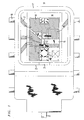
- FIGs. 1 and 2 illustrate a typical optoelectronics package which includes the invention.
- the package, 10 is an optoelectronics package which includes a housing, 11, defining a cavity, 30, for the optoelectronics components.
- the optoelectronics components include a laser, 12, a spherical lens, 13, for focusing the laser light, and a photodetector,14, for monitoring the laser light.
- the components, 12-14 are mounted on a substrate, 15, which is typically silicon.
- the substrate is mounted to the bottom surface of the cavity, 30.
- the silicon substrate, 15, includes metallization, 16, on its surface for providing electrical contact to the components, 12 and 14.
- the metallization, 16, is wire bonded to metallization, 17, on a ledge in the cavity so that the components can be electrically contacted to the outside world through pins, e.g., 18, extending from the sides of the package.
- the metallization, 16 and 17, is typically made of layers of titanium/platinum/gold.
- the cavity, 30, is hermetically sealed by means of a lid, 19, which is bonded to the top surface of the housing by solder, 20 as shown in FIG. 2.
- the laser, 12, is optically coupled to an optical fiber, 22, through an aperture, 21, in a wall, 23, in the cavity,30.
- the cavity, 30, is hermetically sealed by lid, 19, the metallization, 16 and 17, can be subject to delamination by hydrogen gas since the material of the housing, 11, can itself emit hydrogen gas.
- the amount of hydrogen gas within the package ambient can be as high as 1-3 percent of the total internal pressure.
- the cavity includes a member, 31, which in this example is attached to the inner surface of the lid, 19, but could be mounted anywhere in the cavity.
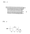
- This member is shown in more detail in FIG. 3.
- the member, 31, includes a layer, 32, which is exposed to the package ambient.
- This layer is preferably a noble metal such as platinum, which typically has a thickness within the range 50 nanometers to 500 nanometers.
- the layer, 32 is formed on another layer or substrate, 33, typically by vacuum evaporation, sputtering, or other means known to those skilled in the art.
- the layer, 33 is a hydride forming material such as titanium or zirconium, and typically has a thickness greater than 200 nanometers.
- the bilayer structure is bonded to the inner surface of the lid, 19, by means of a bonding layer, 34, such as solder.
- a bonding layer, 34 such as solder.
- the two layers, 32 and 33 can be deposited onto the lid by standard techniques, such as vacuum evaporation, sputtering, or other means known to those skilled in the art.
- the member, 31, occupy an area of at least one percent of the interior package area or greater than 10x the total area of exposed at-risk material in the devices to be protected, whichever is the greater.
- At risk material is the material in the package which is susceptible to hydrogen damage.
- the area may be 0.1 - 0.4 cm 2 .
- hydrogen from the package ambient is adsorbed on the surface of the platinum layer, 32, and is transmitted to the interior of that layer by conversion of molecular hydrogen to solvated hydrogen within the metal structure.
- This reaction is endothermic, and in the case of platinum, requires approximately 0.5 eV per H atom as illustrated in the energy diagram of FIG. 4.
- the solvated hydrogen moves into the titanium layer,33, by an exothermic reaction which releases approximately 1.1 eV per atom.
- the solvated hydrogen then precipitates as titanium hydride in another exothermic reaction which releases approximately 0.2 eV per atom.
- the exothermic reactions serve to lock up the hydrogen in the titanium layer, 33, and prevent its return to the platinum layer,32, due to the presence of the energy barrier created thereby.
- the noble metal, 32 prevents the formation of a surface oxide on the reactive (hydride-forming) metal, 33, thereby keeping the surface "open” to admit hydrogen. It may also promote the movement of hydrogen into the hydride-forming metal by the presence of an energy barrier, but that is a secondary function. Thus, the noble metal layer,32 acts as a one way valve for the admission of hydrogen into the hydride forming layer,33.
- the element, 31, was incorporated into several standard pump laser packages by depositing the metals on the package lid and hermetically sealing the package so that the internal ambient was primarily N 2 .
- the packages were then aged for 1840 hours at 100 degrees C. These packages had no detectable hydrogen and no significant amount of water vapor formed within the package housing.
- the hydride forming layer can be an intermetallic compound or alloy such as Iron-Titanium alloys.
- the alloy could be placed in a vacuum chamber where the surface oxide is sputtered off and Pt or Pd deposited on the surface.
- the resulting member could be soldered or mechanically attached to one of the package inner walls or to the lid.
- the layer, 32 was platinum, a palladium layer is also preferred.
Landscapes
- Physics & Mathematics (AREA)
- Condensed Matter Physics & Semiconductors (AREA)
- General Physics & Mathematics (AREA)
- Electromagnetism (AREA)
- Optics & Photonics (AREA)
- Semiconductor Lasers (AREA)
- Optical Couplings Of Light Guides (AREA)
- Casings For Electric Apparatus (AREA)
- Packages (AREA)
Applications Claiming Priority (2)
| Application Number | Priority Date | Filing Date | Title |
|---|---|---|---|
| US08/853,735 US5861665A (en) | 1997-05-13 | 1997-05-13 | Structure for absorption of hydrogen in a package |
| US853735 | 1997-05-13 |
Publications (3)
| Publication Number | Publication Date |
|---|---|
| EP0878845A2 true EP0878845A2 (fr) | 1998-11-18 |
| EP0878845A3 EP0878845A3 (fr) | 2001-07-11 |
| EP0878845B1 EP0878845B1 (fr) | 2002-11-27 |
Family
ID=25316764
Family Applications (1)
| Application Number | Title | Priority Date | Filing Date |
|---|---|---|---|
| EP98303680A Expired - Lifetime EP0878845B1 (fr) | 1997-05-13 | 1998-05-12 | Structure pour l'absorption de hydrogène dans un boítier |
Country Status (5)
| Country | Link |
|---|---|
| US (1) | US5861665A (fr) |
| EP (1) | EP0878845B1 (fr) |
| JP (1) | JPH10322044A (fr) |
| KR (1) | KR19980086954A (fr) |
| DE (1) | DE69809630T2 (fr) |
Cited By (2)
| Publication number | Priority date | Publication date | Assignee | Title |
|---|---|---|---|---|
| WO2006023244A1 (fr) * | 2004-08-23 | 2006-03-02 | Intel Corporation | Event d'hydrogene pour modules microelectroniques avec dispositif resistif thermique (rtd) |
| FR2956521A1 (fr) * | 2010-02-16 | 2011-08-19 | Thales Sa | Dispositif comprenant des composants electriques, electroniques, electromecaniques ou electro-optiques, a sensibilite reduite a faible debit de dose |
Families Citing this family (6)
| Publication number | Priority date | Publication date | Assignee | Title |
|---|---|---|---|---|
| US6203869B1 (en) | 1996-11-12 | 2001-03-20 | Thomas K. Dougherty | Hydrogen getters and methods for fabricating sealed microelectronic packages employing same |
| EP0993047A1 (fr) * | 1998-10-06 | 2000-04-12 | Koninklijke Philips Electronics N.V. | Dispositif semi-conducteur avec des éléments de circuits intégrés du groupe III-V ayant des moyens pour prévenir la pollution par l'hydrogène |
| US6110808A (en) * | 1998-12-04 | 2000-08-29 | Trw Inc. | Hydrogen getter for integrated microelectronic assembly |
| US6923625B2 (en) * | 2002-01-07 | 2005-08-02 | Integrated Sensing Systems, Inc. | Method of forming a reactive material and article formed thereby |
| US20050253283A1 (en) * | 2004-05-13 | 2005-11-17 | Dcamp Jon B | Getter deposition for vacuum packaging |
| CN101163586A (zh) * | 2005-02-17 | 2008-04-16 | 泽斯吸气剂公司 | 柔性多层吸气器 |
Family Cites Families (6)
| Publication number | Priority date | Publication date | Assignee | Title |
|---|---|---|---|---|
| NL7812244A (nl) * | 1978-12-18 | 1980-06-20 | Philips Nv | Halogeengloeilamp. |
| GB8623296D0 (en) * | 1986-09-27 | 1986-10-29 | Emi Plc Thorn | Hydrogen getter |
| US4769345A (en) * | 1987-03-12 | 1988-09-06 | Olin Corporation | Process for producing a hermetically sealed package for an electrical component containing a low amount of oxygen and water vapor |
| US5491361A (en) * | 1994-10-14 | 1996-02-13 | The Aerospace Corporation | Hydrogen out venting electronic package |
| US5624598A (en) * | 1995-04-18 | 1997-04-29 | Shepodd; Timothy J. | Materials for the scavanging of hydrogen at high temperatures |
| US6673400B1 (en) * | 1996-10-15 | 2004-01-06 | Texas Instruments Incorporated | Hydrogen gettering system |
-
1997
- 1997-05-13 US US08/853,735 patent/US5861665A/en not_active Expired - Lifetime
-
1998
- 1998-05-12 DE DE69809630T patent/DE69809630T2/de not_active Expired - Lifetime
- 1998-05-12 KR KR1019980016876A patent/KR19980086954A/ko not_active Withdrawn
- 1998-05-12 EP EP98303680A patent/EP0878845B1/fr not_active Expired - Lifetime
- 1998-05-13 JP JP10129975A patent/JPH10322044A/ja active Pending
Cited By (3)
| Publication number | Priority date | Publication date | Assignee | Title |
|---|---|---|---|---|
| US7377961B2 (en) | 2004-01-12 | 2008-05-27 | Intel Corporation | Hydrogen vent for optoelectronic packages with resistive thermal device (RTD) |
| WO2006023244A1 (fr) * | 2004-08-23 | 2006-03-02 | Intel Corporation | Event d'hydrogene pour modules microelectroniques avec dispositif resistif thermique (rtd) |
| FR2956521A1 (fr) * | 2010-02-16 | 2011-08-19 | Thales Sa | Dispositif comprenant des composants electriques, electroniques, electromecaniques ou electro-optiques, a sensibilite reduite a faible debit de dose |
Also Published As
| Publication number | Publication date |
|---|---|
| KR19980086954A (ko) | 1998-12-05 |
| US5861665A (en) | 1999-01-19 |
| DE69809630T2 (de) | 2003-10-09 |
| EP0878845A3 (fr) | 2001-07-11 |
| EP0878845B1 (fr) | 2002-11-27 |
| JPH10322044A (ja) | 1998-12-04 |
| DE69809630D1 (de) | 2003-01-09 |
Similar Documents
| Publication | Publication Date | Title |
|---|---|---|
| US6369442B1 (en) | Hydrogen getter for integrated microelectronic assembly | |
| EP1835550B1 (fr) | Structure d'emballage pour des dispositifs lumineux à l'état solide et procédé de fabrication correspondant | |
| JP6140259B2 (ja) | マイクロエレクトロニクス、マイクロオプトエレクトロニクスまたはマイクロメカニクスのデバイスのための支持体 | |
| US20070090510A1 (en) | Package structure for solid-state lighting devices and method of fabricating the same | |
| JP3121195B2 (ja) | 無機材料堆積層を有する可撓性高分子フィルムを用いた電池パッケージ及びその製造方法 | |
| CA2447282C (fr) | Support avec depot integre de materiau absorbant les gaz pour la fabrication de dispositifs microelectroniques, microoptoelectroniques et micromecaniques | |
| US20010004534A1 (en) | Diffusion barrier for increased mirror reflectivity in reflective solderable contacts on high power led chip | |
| US5861665A (en) | Structure for absorption of hydrogen in a package | |
| JP7348570B2 (ja) | 発光装置 | |
| US20080290356A1 (en) | Reflective Layered System Comprising a Plurality of Layers that are to be Applied to a III/V Compound Semiconductor Material | |
| JP2021141140A (ja) | 半導体発光素子および電子機器 | |
| JP2001168240A (ja) | 集積型マイクロエレクトロニクスモジュール | |
| CA2480691A1 (fr) | Procede de formation de boitiers dans le cadre de composants electroniques et composants electroniques encapsules hermetiquement | |
| JP3188157B2 (ja) | 半導体レーザ装置用受光素子およびこれを用いた半導体レーザ装置 | |
| KR101172555B1 (ko) | Ⅲ-ⅴ 화합물 반도체 재료 위에 도포될 다수의 층을포함하는 반사성 층 시스템 | |
| Blonder et al. | Article comprising compression bonded parts | |
| JP2002076494A (ja) | 光半導体装置用キャップとこれを用いた光半導体装置 | |
| HK1073336B (en) | Support for microelectronic, microoptoelectronic or micromechanical devices | |
| HK1076539B (en) | Support with integrated deposit of gas absorbing material for manufacturing microelectronic, microoptoelectronic or micromechanical devices |
Legal Events
| Date | Code | Title | Description |
|---|---|---|---|
| PUAI | Public reference made under article 153(3) epc to a published international application that has entered the european phase |
Free format text: ORIGINAL CODE: 0009012 |
|
| AK | Designated contracting states |
Kind code of ref document: A2 Designated state(s): DE FR GB |
|
| AX | Request for extension of the european patent |
Free format text: AL;LT;LV;MK;RO;SI |
|
| PUAL | Search report despatched |
Free format text: ORIGINAL CODE: 0009013 |
|
| AK | Designated contracting states |
Kind code of ref document: A3 Designated state(s): AT BE CH CY DE DK ES FI FR GB GR IE IT LI LU MC NL PT SE |
|
| AX | Request for extension of the european patent |
Free format text: AL;LT;LV;MK;RO;SI |
|
| RIC1 | Information provided on ipc code assigned before grant |
Free format text: 7H 01L 23/26 A, 7H 01S 5/022 B |
|
| RAP1 | Party data changed (applicant data changed or rights of an application transferred) |
Owner name: AGERE SYSTEMS OPTOELECTRONICS GUARDIAN CORPORATION |
|
| 17P | Request for examination filed |
Effective date: 20020109 |
|
| AKX | Designation fees paid |
Free format text: DE FR GB |
|
| GRAG | Despatch of communication of intention to grant |
Free format text: ORIGINAL CODE: EPIDOS AGRA |
|
| 17Q | First examination report despatched |
Effective date: 20020606 |
|
| GRAG | Despatch of communication of intention to grant |
Free format text: ORIGINAL CODE: EPIDOS AGRA |
|
| GRAH | Despatch of communication of intention to grant a patent |
Free format text: ORIGINAL CODE: EPIDOS IGRA |
|
| GRAH | Despatch of communication of intention to grant a patent |
Free format text: ORIGINAL CODE: EPIDOS IGRA |
|
| GRAH | Despatch of communication of intention to grant a patent |
Free format text: ORIGINAL CODE: EPIDOS IGRA |
|
| GRAA | (expected) grant |
Free format text: ORIGINAL CODE: 0009210 |
|
| AK | Designated contracting states |
Kind code of ref document: B1 Designated state(s): DE FR GB |
|
| REG | Reference to a national code |
Ref country code: GB Ref legal event code: FG4D |
|
| REF | Corresponds to: |
Ref document number: 69809630 Country of ref document: DE Date of ref document: 20030109 |
|
| ET | Fr: translation filed | ||
| PLBE | No opposition filed within time limit |
Free format text: ORIGINAL CODE: 0009261 |
|
| STAA | Information on the status of an ep patent application or granted ep patent |
Free format text: STATUS: NO OPPOSITION FILED WITHIN TIME LIMIT |
|
| 26N | No opposition filed |
Effective date: 20030828 |
|
| PGFP | Annual fee paid to national office [announced via postgrant information from national office to epo] |
Ref country code: FR Payment date: 20140509 Year of fee payment: 17 |
|
| PGFP | Annual fee paid to national office [announced via postgrant information from national office to epo] |
Ref country code: GB Payment date: 20150424 Year of fee payment: 18 |
|
| REG | Reference to a national code |
Ref country code: DE Ref legal event code: R082 Ref document number: 69809630 Country of ref document: DE Representative=s name: DILG HAEUSLER SCHINDELMANN PATENTANWALTSGESELL, DE Ref country code: DE Ref legal event code: R081 Ref document number: 69809630 Country of ref document: DE Owner name: AVAGO TECHNOLOGIES GENERAL IP (SINGAPORE) PTE., SG Free format text: FORMER OWNER: AGERE SYSTEMS OPTOELECTRONICS GUARDIAN CORP., ORLANDO, FLA., US |
|
| REG | Reference to a national code |
Ref country code: FR Ref legal event code: ST Effective date: 20160129 |
|
| PG25 | Lapsed in a contracting state [announced via postgrant information from national office to epo] |
Ref country code: FR Free format text: LAPSE BECAUSE OF NON-PAYMENT OF DUE FEES Effective date: 20150601 |
|
| GBPC | Gb: european patent ceased through non-payment of renewal fee |
Effective date: 20160512 |
|
| PG25 | Lapsed in a contracting state [announced via postgrant information from national office to epo] |
Ref country code: GB Free format text: LAPSE BECAUSE OF NON-PAYMENT OF DUE FEES Effective date: 20160512 |
|
| PGFP | Annual fee paid to national office [announced via postgrant information from national office to epo] |
Ref country code: DE Payment date: 20170420 Year of fee payment: 20 |
|
| REG | Reference to a national code |
Ref country code: DE Ref legal event code: R071 Ref document number: 69809630 Country of ref document: DE |