EP0879841A2 - Composé de silicium, procédé pour sa préparation et dispositif électroluminescent contenant ce composé - Google Patents
Composé de silicium, procédé pour sa préparation et dispositif électroluminescent contenant ce composé Download PDFInfo
- Publication number
- EP0879841A2 EP0879841A2 EP98303883A EP98303883A EP0879841A2 EP 0879841 A2 EP0879841 A2 EP 0879841A2 EP 98303883 A EP98303883 A EP 98303883A EP 98303883 A EP98303883 A EP 98303883A EP 0879841 A2 EP0879841 A2 EP 0879841A2
- Authority
- EP
- European Patent Office
- Prior art keywords
- group
- substituted
- silicon compound
- unsubstituted
- compound according
- Prior art date
- Legal status (The legal status is an assumption and is not a legal conclusion. Google has not performed a legal analysis and makes no representation as to the accuracy of the status listed.)
- Granted
Links
- VJHLHGFTPAGQSG-UHFFFAOYSA-N CCC(C)(C)NN Chemical compound CCC(C)(C)NN VJHLHGFTPAGQSG-UHFFFAOYSA-N 0.000 description 1
Images

Classifications
-
- C—CHEMISTRY; METALLURGY
- C08—ORGANIC MACROMOLECULAR COMPOUNDS; THEIR PREPARATION OR CHEMICAL WORKING-UP; COMPOSITIONS BASED THEREON
- C08G—MACROMOLECULAR COMPOUNDS OBTAINED OTHERWISE THAN BY REACTIONS ONLY INVOLVING UNSATURATED CARBON-TO-CARBON BONDS
- C08G77/00—Macromolecular compounds obtained by reactions forming a linkage containing silicon with or without sulfur, nitrogen, oxygen or carbon in the main chain of the macromolecule
- C08G77/60—Macromolecular compounds obtained by reactions forming a linkage containing silicon with or without sulfur, nitrogen, oxygen or carbon in the main chain of the macromolecule in which all the silicon atoms are connected by linkages other than oxygen atoms
-
- C—CHEMISTRY; METALLURGY
- C07—ORGANIC CHEMISTRY
- C07F—ACYCLIC, CARBOCYCLIC OR HETEROCYCLIC COMPOUNDS CONTAINING ELEMENTS OTHER THAN CARBON, HYDROGEN, HALOGEN, OXYGEN, NITROGEN, SULFUR, SELENIUM OR TELLURIUM
- C07F7/00—Compounds containing elements of Groups 4 or 14 of the Periodic Table
- C07F7/02—Silicon compounds
- C07F7/08—Compounds having one or more C—Si linkages
- C07F7/0896—Compounds with a Si-H linkage
-
- H—ELECTRICITY
- H10—SEMICONDUCTOR DEVICES; ELECTRIC SOLID-STATE DEVICES NOT OTHERWISE PROVIDED FOR
- H10K—ORGANIC ELECTRIC SOLID-STATE DEVICES
- H10K85/00—Organic materials used in the body or electrodes of devices covered by this subclass
- H10K85/40—Organosilicon compounds, e.g. TIPS pentacene
-
- H—ELECTRICITY
- H10—SEMICONDUCTOR DEVICES; ELECTRIC SOLID-STATE DEVICES NOT OTHERWISE PROVIDED FOR
- H10K—ORGANIC ELECTRIC SOLID-STATE DEVICES
- H10K50/00—Organic light-emitting devices
- H10K50/10—OLEDs or polymer light-emitting diodes [PLED]
- H10K50/11—OLEDs or polymer light-emitting diodes [PLED] characterised by the electroluminescent [EL] layers
-
- H—ELECTRICITY
- H10—SEMICONDUCTOR DEVICES; ELECTRIC SOLID-STATE DEVICES NOT OTHERWISE PROVIDED FOR
- H10K—ORGANIC ELECTRIC SOLID-STATE DEVICES
- H10K85/00—Organic materials used in the body or electrodes of devices covered by this subclass
- H10K85/10—Organic polymers or oligomers
-
- H—ELECTRICITY
- H10—SEMICONDUCTOR DEVICES; ELECTRIC SOLID-STATE DEVICES NOT OTHERWISE PROVIDED FOR
- H10K—ORGANIC ELECTRIC SOLID-STATE DEVICES
- H10K85/00—Organic materials used in the body or electrodes of devices covered by this subclass
- H10K85/10—Organic polymers or oligomers
- H10K85/111—Organic polymers or oligomers comprising aromatic, heteroaromatic, or aryl chains, e.g. polyaniline, polyphenylene or polyphenylene vinylene
-
- H—ELECTRICITY
- H10—SEMICONDUCTOR DEVICES; ELECTRIC SOLID-STATE DEVICES NOT OTHERWISE PROVIDED FOR
- H10K—ORGANIC ELECTRIC SOLID-STATE DEVICES
- H10K85/00—Organic materials used in the body or electrodes of devices covered by this subclass
- H10K85/30—Coordination compounds
- H10K85/321—Metal complexes comprising a group IIIA element, e.g. Tris (8-hydroxyquinoline) gallium [Gaq3]
- H10K85/324—Metal complexes comprising a group IIIA element, e.g. Tris (8-hydroxyquinoline) gallium [Gaq3] comprising aluminium, e.g. Alq3
-
- H—ELECTRICITY
- H10—SEMICONDUCTOR DEVICES; ELECTRIC SOLID-STATE DEVICES NOT OTHERWISE PROVIDED FOR
- H10K—ORGANIC ELECTRIC SOLID-STATE DEVICES
- H10K85/00—Organic materials used in the body or electrodes of devices covered by this subclass
- H10K85/60—Organic compounds having low molecular weight
-
- H—ELECTRICITY
- H10—SEMICONDUCTOR DEVICES; ELECTRIC SOLID-STATE DEVICES NOT OTHERWISE PROVIDED FOR
- H10K—ORGANIC ELECTRIC SOLID-STATE DEVICES
- H10K85/00—Organic materials used in the body or electrodes of devices covered by this subclass
- H10K85/60—Organic compounds having low molecular weight
- H10K85/615—Polycyclic condensed aromatic hydrocarbons, e.g. anthracene
-
- H—ELECTRICITY
- H10—SEMICONDUCTOR DEVICES; ELECTRIC SOLID-STATE DEVICES NOT OTHERWISE PROVIDED FOR
- H10K—ORGANIC ELECTRIC SOLID-STATE DEVICES
- H10K85/00—Organic materials used in the body or electrodes of devices covered by this subclass
- H10K85/60—Organic compounds having low molecular weight
- H10K85/615—Polycyclic condensed aromatic hydrocarbons, e.g. anthracene
- H10K85/621—Aromatic anhydride or imide compounds, e.g. perylene tetra-carboxylic dianhydride or perylene tetracarboxylic di-imide
-
- H—ELECTRICITY
- H10—SEMICONDUCTOR DEVICES; ELECTRIC SOLID-STATE DEVICES NOT OTHERWISE PROVIDED FOR
- H10K—ORGANIC ELECTRIC SOLID-STATE DEVICES
- H10K85/00—Organic materials used in the body or electrodes of devices covered by this subclass
- H10K85/60—Organic compounds having low molecular weight
- H10K85/631—Amine compounds having at least two aryl rest on at least one amine-nitrogen atom, e.g. triphenylamine
-
- H—ELECTRICITY
- H10—SEMICONDUCTOR DEVICES; ELECTRIC SOLID-STATE DEVICES NOT OTHERWISE PROVIDED FOR
- H10K—ORGANIC ELECTRIC SOLID-STATE DEVICES
- H10K85/00—Organic materials used in the body or electrodes of devices covered by this subclass
- H10K85/60—Organic compounds having low molecular weight
- H10K85/649—Aromatic compounds comprising a hetero atom
-
- H—ELECTRICITY
- H10—SEMICONDUCTOR DEVICES; ELECTRIC SOLID-STATE DEVICES NOT OTHERWISE PROVIDED FOR
- H10K—ORGANIC ELECTRIC SOLID-STATE DEVICES
- H10K85/00—Organic materials used in the body or electrodes of devices covered by this subclass
- H10K85/60—Organic compounds having low molecular weight
- H10K85/649—Aromatic compounds comprising a hetero atom
- H10K85/656—Aromatic compounds comprising a hetero atom comprising two or more different heteroatoms per ring
- H10K85/6565—Oxadiazole compounds
-
- Y—GENERAL TAGGING OF NEW TECHNOLOGICAL DEVELOPMENTS; GENERAL TAGGING OF CROSS-SECTIONAL TECHNOLOGIES SPANNING OVER SEVERAL SECTIONS OF THE IPC; TECHNICAL SUBJECTS COVERED BY FORMER USPC CROSS-REFERENCE ART COLLECTIONS [XRACs] AND DIGESTS
- Y10—TECHNICAL SUBJECTS COVERED BY FORMER USPC
- Y10S—TECHNICAL SUBJECTS COVERED BY FORMER USPC CROSS-REFERENCE ART COLLECTIONS [XRACs] AND DIGESTS
- Y10S428/00—Stock material or miscellaneous articles
- Y10S428/917—Electroluminescent
-
- Y—GENERAL TAGGING OF NEW TECHNOLOGICAL DEVELOPMENTS; GENERAL TAGGING OF CROSS-SECTIONAL TECHNOLOGIES SPANNING OVER SEVERAL SECTIONS OF THE IPC; TECHNICAL SUBJECTS COVERED BY FORMER USPC CROSS-REFERENCE ART COLLECTIONS [XRACs] AND DIGESTS
- Y10—TECHNICAL SUBJECTS COVERED BY FORMER USPC
- Y10T—TECHNICAL SUBJECTS COVERED BY FORMER US CLASSIFICATION
- Y10T428/00—Stock material or miscellaneous articles
- Y10T428/31504—Composite [nonstructural laminate]
- Y10T428/31652—Of asbestos
- Y10T428/31663—As siloxane, silicone or silane
Definitions
- the present invention relates to a novel silicon compound, a method for making the same, and an electroluminescent device using the same.
- High performance electronic devices require materials for effectively transporting only electrons or holes.
- Hole-transporting materials which transport only holes at a high efficiency have been widely used for electrophotographic photosensitive members and are expected as organic luminescent materials.
- OPC organic photoconductive
- OPC materials have advantages in safety and productivity and costs compared to inorganic photosensitive materials, and have been vigorously used for copying machines and printers.
- the OPC members generally have a multilayered structure of a charge generation layer (CGL) and a charge transport layer (CTL).
- the CTL is formed by coating a dispersion of a low molecule charge transport material (CTM), e.g. a triarylamine, hydrazone or dialkylaminobenzene derivative, in a transparent polymeric film, such as a polycarbonate resin.
- CTM low molecule charge transport material
- the concentration of the CTM in the polymer matrix is limited since the CTM crystal deposits at a high concentration.
- hole transferability decreases as the concentration decreases.
- the CTL is fragile and has a low tensile strength. Such low mechanical strength causes scratches and cracks on the OPC member, resulting in image defects.
- Exemplary polymeric charge transport materials are polystyrenes having hydrazone groups which are disclosed in Japanese Patent Laid-Open Nos. 2-272005 and 3-180852. These materials are formed into a film with great difficulty, and have unsatisfactory hole transport rates and residual potentials.
- Examples of disclosed organic hosts include naphthalene, anthracene, phenanthrene, tetracene, pyrene, benzpyrene, chrysene, picene, carbazole, fluorene, biphenyl, terphenyl, triphenylene oxide, dihalobiphenyl, transstilbene, and 1,4-diphenylbutadiene.
- Examples of disclosed activators include anthracene, tetracene and pentacene.
- Tang et al. developed an EL device having a high luminance for a low driving voltage ( Appl. Phys. Lett., 51 , 913 (1987) and U.S. Patent No. 4,356,429).
- the EL device is fabricated by depositing two significantly thin layers, that is, a charge transport layer and a luminescent layer, between the positive electrode and the negative electrode by a vacuum deposition process.
- Such layered organic EL devices are disclosed in, for example, Japanese Patent Laid-Open Nos. 59-194393, 3-264692, and 3-163188, U.S. Patent Nos. 4,539,507 and 4,720,432, and Appl. Phys. Lett., 55 , 1467 (1989).
- an EL device of a triple-layered structure having independently a carrier transport function and a luminescent function was disclosed in Jpn. J. Apply. Phys., 27 , L269 and L713 (1988). Since the carrier transportability is improved in such an EL device, the versatility of possible dyes in the luminescent layer is considerably increased. Further, the device configuration suggests feasibility of improved luminescence by effectively trapping holes and electrons (or excimers) in the central luminescent layer.
- Monolithic organic EL devices are generally formed by vacuum deposition processes. EL devices having considerable luminance are also formed by casting processes (as described in, for example, Extended Abstracts (The 50th Autumn Meeting (1989), p. 1006 and The 51st Autumn Meeting (1990), p. 1041; The Japan Society of Applied Physics).
- EL devices having considerable luminance are also formed by casting processes (as described in, for example, Extended Abstracts (The 50th Autumn Meeting (1989), p. 1006 and The 51st Autumn Meeting (1990), p. 1041; The Japan Society of Applied Physics).
- Considerably high luminance is also achieved by a single-layered mixture-type EL device, in which the layer is formed by immersion-coating a solution containing polyvinyl carbazole as a hole transport compound, an oxadiazole derivative as a charge transport compound and coumarin-6 as a luminescent material (as described in Extended Abstracts (The 38th Spring Meeting (1991), p. 1086; The Japan Society of Applied Physics and
- the organic EL devices have been significantly improved and have suggested feasibility of a wide variety of applications; however, these EL devices have some problems for practical use, for example, insufficient luminance, a change in luminance during use for a long period, and deterioration by atmospheric gas containing oxygen and humidity. Accordingly, a novel material not having such disadvantages and an electroluminescent device have been eagerly awaited.
- An aspect of the present invention is a silicon compound having a repeating unit represented by the following general formula (1): wherein R is a hydrogen atom, a straight or branched alkyl group having 1 to 20 carbon atoms, a substituted or unsubstituted aryl group, or a substituted or unsubstituted heterocyclic group, Ar is a substituted or unsubstituted aryl group or an unsubstituted heterocyclic group, m is an integer of 2 or more, and n is an integer of 5,000 or less.
- a further aspect of the present invention is an electroluminescent device comprising a pair of electrodes and an organic compound layer interposed between said electrodes, said organic compound layer comprising a silicon compound having a repeating unit represented by the following general formula (1): wherein R is a hydrogen atom, a straight or branched alkyl group having 1 to 20 carbon atoms, a substituted or unsubstituted aryl group, or a substituted or unsubstituted heterocyclic group, Ar is a substituted or unsubstituted aryl group or an unsubstituted heterocyclic group, m is an integer of 2 or more, and n is an integer of 5,000 or less.
- R is a hydrogen atom, a straight or branched alkyl group having 1 to 20 carbon atoms, a substituted or unsubstituted aryl group, or a substituted or unsubstituted heterocyclic group
- Ar is a substituted or unsubstituted aryl group
- the silicon compound in accordance with the present invention has excellent charge transport characteristics and can form a uniform and smooth film, hence it is useful as a charge transport material.
- the method in accordance with the present invention enables ready production of the silicon compound.
- the electroluminescent device in accordance with the present invention has high luminance at a low voltage for long periods, and can emit a variety of hues.
- the electroluminescent device can emit primaries, i.e., red, blue and green; hence it can be used in displays.
- the device can be produced by a vacuum deposition or casting process at low production costs.
- the present inventors have studied intensively towards the resolution of problems caused by the charge transport material in the electroluminescent device, and have discovered that a silicon compound having a polysilane main chain and aryl groups has excellent charge transport characteristics and film formability and the resulting film has excellent stability.
- the present invention is completed under such findings.
- the silicon compound in accordance with the present invention is represented by the following general formula (1):
- R is a hydrogen atom, a straight or branched alkyl group having 1 to 20 carbon atoms and preferably 1 to 10, a substituted or unsubstituted aryl group, or a substituted or unsubstituted heterocyclic group.
- straight or branched alkyl groups having 1 to 20 carbon atoms include straight alkyl groups, such as methyl, ethyl, propyl, hexyl and octyl groups, and branched alkyl groups, such as isopropyl and isobutyl groups.
- unsubstituted aryl groups include polycyclic aryl groups, such as phenyl, biphenyl and terphenyl groups, and fused-ring aryl groups, such as naphthyl and anthranyl groups.
- unsubstituted heterocyclic groups include 6- and 5-membered rings, such as pyridyl, furyl, thienyl and pyrrolyl, and fused-ring heterocyclic groups such as acrydinyl.
- each of the above-mentioned aryl and heterocyclic groups has a substituent group.
- substituent groups include halogen atoms, e.g.
- alkyl groups e.g. methyl and ethyl groups; alkoxyl groups, e.g. methoxy and ethoxy groups; aryloxyl groups, e.g. a phenoxy group; primary and secondary amino groups; a nitro group; aryl groups, e.g. phenyl and tolyl groups; and aralkyl groups, e.g. benzyl and phenethyl groups.
- m is an integer of 2 or more and preferably 2 to 20
- n is an integer of 5,000 or less and preferably 30 to 1,000. Although the values of m and n are not limited to these ranges, these values are preferred in view of reactivity and yield in the production of the compound.
- Ar is a substituted or unsubstituted aryl group or an unsubstituted heterocyclic group. Examples of such groups are as follows:
- Ar 2 and Ar 3 each represents a substituted or unsubstituted aryl group or a substituted or unsubstituted heterocyclic group.
- unsubstituted aryl groups include phenyl; polycyclic aryl groups, e.g. biphenyl and terphenyl groups; and fused-ring aryl groups, e.g. naphthyl and anthranyl groups.
- unsubstituted heterocyclic groups include 6- and 5-member heterocyclic groups, e.g. pyridyl, furyl, thienyl and pyrrolyl groups; and fused-ring heterocyclic groups, e.g. acrydinyl.
- each of the above-mentioned aryl and heterocyclic groups has a substituent group.
- substituent groups include halogen atoms, e.g. chlorine and bromine; alkyl groups, e.g. methyl and ethyl groups; alkoxyl groups, e.g. methoxy and ethoxy groups; aryloxyl groups, e.g. a phenoxy group; primary and secondary amino groups; a nitro group; aryl groups, e.g. phenyl and tolyl groups; aralkyl groups, e.g. benzyl and phenethyl groups; and alkenyl groups, e.g. formyl, acetyl and vinyl groups.
- a silicon compound having the repeating unit of formula (1) is terminated by an appropriate terminal group.
- the silicon compound is terminated with the group:
- the silicon compound of formula (1) has the formula:
- the silicon compound in accordance with the present invention represented by the formula (1) is synthesized by the reaction of a polysilane compound with a compound having any one of the groups (I) to (III).
- the reaction is preferably performed in the presence of a catalyst, such as platinum chloride acid hydrate.
- the process of synthesis of the silicon compound is now described.
- the molar ratio, the compound of the formula (2) : the compound of the formula (3), is preferably in a range of 1.0:10 to 10:1.0. It is preferable that the platinum chloride acid hydrate catalysis be added in an amount of 0.1 to 0.01 mole to 1 mole of the compound of the formula (2).
- the reaction is performed in a solvent such as tetrahydrofuran at a temperature of 20 to 66 °C for a time of 3 to 10 hours.
- the electroluminescent device in accordance with the present invention comprises a pair of electrodes and an organic layer composed of the silicon compound represented by the formula (1) displaced between the electrodes.
- the silicon compound is formed between the positive and negative electrodes by a vacuum deposition or solution coating process.
- the thickness of the organic layer is preferably 2 ⁇ m or less, more preferably 0.5 ⁇ m or less, and most preferably 0.05 ⁇ m to 0.5 ⁇ m.
- a plurality of layers may be provided between the two electrodes.
- at least one layer among these layers is composed of the compound represented by the formula (1).
- the luminescent color of the electroluminescent device can be determined by selecting the compound represented by the formula (1).
- Fig. 1 is a schematic cross-sectional view of an embodiment of the electroluminescent device in accordance with the present invention.
- a positive electrode 2, a luminescent layer 3 and a negative electrode 4 are formed on a substrate 1 in that order.
- the luminescent layer 3 may be composed of a single compound having hole transportability, electron transportability and luminescence, or a mixture of compounds each having one of these properties.
- Fig. 2 is a schematic cross-sectional view of another embodiment of the electroluminescent device in accordance with the present invention.
- a positive electrode 2, a hole transport layer 5, an electron transport layer 6 and a negative electrode 4 are formed on a substrate 1 in that order.
- the hole transport layer 5 and the electron transport layer 6 form a luminescent layer 3.
- the hole transport layer 5 may be composed of a luminescent material having hole transportability or a mixture including such a material and a non-luminescent material having hole transportability.
- the luminescent and non-luminescent materials may also have electron transportability.
- the electron transport layer 6 may be composed of a luminescent material having electron transportability or a mixture including such a material and a non-luminescent material having electron transportability.
- the luminescent and non-luminescent materials may also have hole transportability.
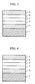
- Fig. 3 is a schematic cross-sectional view of a further embodiment of the electroluminescent device in accordance with the present invention.
- a positive electrode 2, a hole transport layer 5, a luminescent layer 3, an electron transport layer 6 and a negative electrode 4 are formed on a substrate 1 in that order.
- carrier transport and luminescence are performed in the individual layers.
- Such a configuration permits a wide variety of combinations of a material having excellent hole transportability, a material having excellent electron transportability and a material having excellent luminescence.
- the configuration permits the use of various compounds emitting light with different wavelengths; hence the hue of the luminescent light can be controlled within a wide range. Trapping effectively holes and electrons (or excimers) in the central luminescent layer will increase the luminescent efficiency.
- Fig. 4 is a schematic cross-sectional view of a still further embodiment of the electroluminescent device in accordance with the present invention.
- a positive electrode 2, a hole injection/transport layer 7, a hole transport layer 5, an electron transport layer 6 and a negative electrode 4 are formed on a substrate 1 in that order.
- the silicon compound in accordance with the present invention represented by the formula (1) has excellent luminescence compared to known compounds, and can be used for the electroluminescent devices shown in Figs. 1 to 4.
- the silicon compound represented by the formula (1) has hole transportability and/or carrier transportability depending on the types of the substituent groups.
- a silicon compound or a combination of different silicon compounds may be used in the configurations shown in Figs. 1 to 4.
- another layer or other layers can be provided in addition to at least one silicon compound layer.
- the silicon compound represented by the formula (1) is used as a constituent in the luminescent layer or a charge transport layer. These layers may further include various compounds used in electrophotographic photosensitive members. Examples of the compounds include hole transport materials, luminescent hole transport materials (for example, compounds shown in Tables 1 to 5), electron transport materials, and luminescent electron transport materials (for example, compounds shown in Tables 6 to 9).
- Table 10 illustrates examples of dopant dyes. The addition of a trace amount of dopant dye in the luminescent layer will significantly increase the luminescent efficiency or will change the luminescent color.
- each layer on the substrate is formed by a vacuum deposition process or a coating process using a combination of the relevant compound and a suitable binding resin.
- Non-limiting examples of the binding resins include polyvinyl carbazole resins, polycarbonate resins, polyester resins, polyarylate resins, butyral resins, polystyrene resins, polyvinyl acetal resins, diallyl phthalate resins, acrylate resins, methacrylate resins, phenol resins, epoxy resins, silicon resins, polysulfone resins, and urea resins.
- binding resins can be used alone or in combination.
- Materials for the positive electrode have preferably large work functions.
- preferred materials include nickel, gold, platinum, palladium, selenium, rhenium, and iridium, alloys thereof, tin oxide, indium tin oxide (ITO), and copper iodide.
- conductive polymers such as poly(3-methylthiophene), polyphenylene sulfide and polypyrrole, can be used.
- Preferred materials for the negative electrode have small work functions. Examples of such materials include silver, lead, tin, magnesium, aluminum, calcium, manganese, indium and chromium, and alloys thereof.
- At least one of the materials for the positive and negative electrodes has a transmittance of at least 50% at the wavelength range of the light emerging from the electroluminescent device.
- Examples of transparent substrates used in the present invention include glass plates and plastic films.
- the silicon compound in accordance with the present invention represented by the formula (1) has excellent hole transportability and can form a uniform and smooth film, it is suitable for a hole transport material in an organic EL device.
- a film was formed as in Example 4, but the following compound was used instead of Compound 139 or 145.
- the coating layer had some cracks and a rough surface.
- ITO indium tin oxide
- a coating solution 0.20 g of Compound 8 was dissolved into 10 ml of THF to prepare a coating solution, and then the coating solution was applied onto the transparent substrate by a spin coating process to form a coating layer with a thickness of 110 nm.
- An aluminum electrode with a thickness of 200 nm was deposited by a vacuum deposition process to form a device having the configuration shown in Fig. 1.
- a direct current of 10 V was applied between the ITO positive electrode and the Al negative electrode.
- a current flow of 12 mA/cm 2 and a blue luminescence with a luminance of 200 cd/m 2 were observed.
- a transparent glass substrate provided with an ITO layer having a thickness of 100 nm deposited by a sputtering process was cleaned with deionized water and isopropyl alcohol.
- 0.20 g of methylphenylpolysilane (weight average molecular weight: 30,000) was dissolved into 10 ml of THF to prepare a coating solution.
- the coating solution was applied onto the transparent substrate by a dip coating process to form a coating layer with a thickness of 110 nm.
- An aluminum electrode with a thickness of 200 nm was deposited thereon by a vacuum deposition process to form a device having the configuration shown in Fig. 1.
- a direct current of 12 V was applied between the ITO positive electrode and the Al negative electrode.
- a current flow of 0.150 mA/cm 2 and no luminescence were observed.
- a transparent glass substrate provided with an ITO layer having a thickness of 100 nm deposited by a sputtering process was cleaned with deionized water and isopropyl alcohol.
- 0.50 g of Compound 61 was dissolved into 25 ml of THF to prepare a coating solution.
- the coating solution was applied onto the transparent substrate by a dip coating process to form a coating layer with a thickness of 60 nm as a hole transport layer.
- An aluminum quinolinol layer with a thickness of 50 nm as an electron transport layer was deposited thereon by a vacuum deposition process.
- a direct current of 7 V was applied between the ITO positive electrode and the Mg/Ag negative electrode.
- a current flow of 11 mA/cm 2 and a green luminescence having a luminance of 265 cd/m 2 were observed.
- a voltage with a current density of 10 mA/cm 2 was applied to the sample for 2,000 hours. The luminance was 250 cd/m 2 at the start and changed to 225 cd/m 2 at the end.
- a transparent glass substrate provided with an ITO layer having a thickness of 100 nm deposited by a sputtering process was cleaned with deionized water and isopropyl alcohol.
- 0.20 g of vinylcarbazole was dissolved into 15 ml of THF to prepare a coating solution.
- the coating solution was applied onto the transparent substrate by a spin coating process to form a coating layer with a thickness of 40 nm as a hole transport layer.
- a coating solution containing 0.20 g of Compound 100 in 20 ml of THF was applied thereon by a spin coating process to form a luminescent layer with a thickness of 15 nm.
- An aluminum quinolinol layer with a thickness of 50 nm as an electron transport layer was deposited thereon by a vacuum deposition process.
- a direct current of 12 V was applied between the ITO positive electrode and the Al/Li negative electrode.
- a current flow of 25 mA/cm 2 and a green luminescence having a luminance of 330 cd/m 2 were observed.
- a voltage with a current density of 15 mA/cm 2 was applied to the sample for 2,000 hours. The luminance was 250 cd/m 2 at the start and changed to 213 cd/m 2 at the end.
- a transparent glass substrate provided with an ITO layer having a thickness of 100 nm deposited by a sputtering process was cleaned with deionized water and isopropyl alcohol.
- 0.20 g of Compound 88 was dissolved into 15 ml of THF to prepare a coating solution.
- the coating solution was applied onto the transparent substrate by a spin coating process to form a coating layer with a thickness of 30 nm as a hole injection/transport layer.
- a hole transport layer with a thickness of 20 nm composed of ⁇ -NPD (N,N'-Diphenyl-N,N'-di(naphthyl)-4,4'-diamino-biphenyl) represented by the formula (5) and an electron transport layer with a thickness of 50 nm composed of an aluminum quinolinol layer were deposited thereon by a vacuum deposition process in that order.
- An aluminum electrode was deposited thereon by a vacuum deposition process to form a device having the configuration shown in Fig. 4.
- a direct current of 10 V was applied between the ITO positive electrode and the Al negative electrode.
- a current flow of 21 mA/cm 2 and a green luminescence having a luminance of 425 cd/m 2 were observed.
- a voltage with a current density of 11 mA/cm 2 was applied to the sample for 2,000 hours. The luminance was 250 cd/m 2 at the start and changed to 230 cd/m 2 at the end.
- a transparent glass substrate provided with an ITO layer having a thickness of 100 nm deposited by a sputtering process was cleaned with deionized water and isopropyl alcohol.
- 0.50 g of Compound 139 was dissolved into 25 ml of THF to prepare a coating solution.
- the coating solution was applied onto the transparent substrate by a dip coating process to form a coating layer with a thickness of 60 nm as a hole transport layer.
- An aluminum quinolinol layer with a thickness of 50 nm as an electron transport layer was deposited thereon by a vacuum deposition process.
- a direct current of 8 V was applied between the ITO positive electrode and the Mg/Ag negative electrode.
- a current flow of 13 mA/cm 2 and a green luminescence having a luminance of 470 cd/m 2 were observed.
- a voltage with a current density of 5 mA/cm 2 was applied to the sample for 2,000 hours. The luminance was 250 cd/m 2 at the start and changed to 220 cd/m 2 at the end.
- ITO layer with a thickness of 100 nm was deposited on a glass plate by a sputtering process, and the resulting transparent substrate was cleaned with deionized water and isopropyl alcohol.
- 0.20 g of Compound 104 was dissolved into 10 ml of THF to prepare a coating solution, and then the coating solution was applied onto the transparent substrate by a spin coating process to form a coating layer with a thickness of 100 nm.
- An aluminum electrode with a thickness of 200 nm was deposited thereon by a vacuum deposition process to form a device having the configuration shown in Fig. 1.
- a direct current of 12 V was applied between the ITO positive electrode and the A1 negative electrode.
- a current flow of 15 mA/cm 2 and a red luminescence with a luminance of 210 cd/m 2 were observed.
Landscapes
- Chemical & Material Sciences (AREA)
- Organic Chemistry (AREA)
- Health & Medical Sciences (AREA)
- Chemical Kinetics & Catalysis (AREA)
- Medicinal Chemistry (AREA)
- Polymers & Plastics (AREA)
- Engineering & Computer Science (AREA)
- Materials Engineering (AREA)
- Electroluminescent Light Sources (AREA)
- Silicon Polymers (AREA)
- Photoreceptors In Electrophotography (AREA)
Applications Claiming Priority (6)
| Application Number | Priority Date | Filing Date | Title |
|---|---|---|---|
| JP142956/97 | 1997-05-19 | ||
| JP14295697 | 1997-05-19 | ||
| JP14295697 | 1997-05-19 | ||
| JP13263598 | 1998-04-28 | ||
| JP13263598A JPH1135688A (ja) | 1997-05-19 | 1998-04-28 | 珪素含有化合物、該珪素含有化合物の製造方法及び該珪素含有化合物を用いた発光素子 |
| JP132635/98 | 1998-04-28 |
Publications (3)
| Publication Number | Publication Date |
|---|---|
| EP0879841A2 true EP0879841A2 (fr) | 1998-11-25 |
| EP0879841A3 EP0879841A3 (fr) | 1999-07-14 |
| EP0879841B1 EP0879841B1 (fr) | 2002-10-30 |
Family
ID=26467163
Family Applications (1)
| Application Number | Title | Priority Date | Filing Date |
|---|---|---|---|
| EP19980303883 Expired - Lifetime EP0879841B1 (fr) | 1997-05-19 | 1998-05-14 | Composé de silicium, procédé pour sa préparation et dispositif électroluminescent contenant ce composé |
Country Status (4)
| Country | Link |
|---|---|
| US (2) | US6534198B1 (fr) |
| EP (1) | EP0879841B1 (fr) |
| JP (1) | JPH1135688A (fr) |
| DE (1) | DE69808986D1 (fr) |
Families Citing this family (18)
| Publication number | Priority date | Publication date | Assignee | Title |
|---|---|---|---|---|
| JPH1135687A (ja) * | 1997-07-17 | 1999-02-09 | Sumitomo Chem Co Ltd | ポリシラン共重合体、その製造方法、それを用いた有機エレクトロルミネッセンス素子及び電子写真感光体 |
| JP2003197377A (ja) * | 2001-10-18 | 2003-07-11 | Fuji Xerox Co Ltd | 有機電界発光素子 |
| US20050051758A1 (en) * | 2003-09-09 | 2005-03-10 | Michiharu Yamamoto | Photorefractive composition |
| US20050116209A1 (en) * | 2003-10-06 | 2005-06-02 | Michiharu Yamamoto | Image correction device |
| WO2005060624A2 (fr) * | 2003-12-10 | 2005-07-07 | Northwestern University | Compositions de couche de transport de trou et dispositifs a diodes relatifs |
| US7250121B2 (en) * | 2004-05-13 | 2007-07-31 | Nitto Denko Corporation | Non-linear optical device material composition |
| US20050253120A1 (en) * | 2004-05-13 | 2005-11-17 | Michiharu Yamamoto | Non-linear optical device material composition |
| US7344811B2 (en) * | 2004-10-28 | 2008-03-18 | Samsung Electronic Co., Ltd. | Polysilane-based charge transport materials |
| US7317058B2 (en) * | 2004-11-01 | 2008-01-08 | Nitto Denko Corporation | (Meth)acrylate polymer and non-linear optical device material composition |
| US8057908B2 (en) * | 2004-11-15 | 2011-11-15 | Northwestern University | Hole transport layer compositions and related diode devices |
| JP5296961B2 (ja) * | 2005-09-12 | 2013-09-25 | 大阪瓦斯株式会社 | コポリシラン及びこのコポリシランを含む樹脂組成物 |
| KR101308790B1 (ko) * | 2005-12-07 | 2013-09-17 | 오사까 가스 가부시키가이샤 | 폴리실란 및 폴리실란을 함유하는 수지 조성물 |
| JP5421772B2 (ja) * | 2006-07-25 | 2014-02-19 | 日東電工株式会社 | 長時間の回折格子持続性を有する非線形光学装置 |
| WO2008013775A2 (fr) * | 2006-07-25 | 2008-01-31 | Nitto Denko Corporation | Dispositif optique non linéaire sensible au laser vert |
| EP2252913A1 (fr) * | 2008-02-05 | 2010-11-24 | Nitto Denko Corporation | Dispositifs optiques réactifs au laser bleu et procédé de modulation de la lumière |
| GB2463040B (en) | 2008-08-28 | 2012-10-31 | Cambridge Display Tech Ltd | Light-emitting material |
| US20100096603A1 (en) * | 2008-10-20 | 2010-04-22 | Nitto Denko Corporation | Optical devices responsive to near infrared laser and methods of modulating light |
| US20100099789A1 (en) * | 2008-10-20 | 2010-04-22 | Nitto Denko Corporation | Method for modulating light of photorefractive composition |
Family Cites Families (24)
| Publication number | Priority date | Publication date | Assignee | Title |
|---|---|---|---|---|
| US3172862A (en) | 1960-09-29 | 1965-03-09 | Dow Chemical Co | Organic electroluminescent phosphors |
| US3220972A (en) * | 1962-07-02 | 1965-11-30 | Gen Electric | Organosilicon process using a chloroplatinic acid reaction product as the catalyst |
| US3173050A (en) | 1962-09-19 | 1965-03-09 | Dow Chemical Co | Electroluminescent cell |
| US3710167A (en) | 1970-07-02 | 1973-01-09 | Rca Corp | Organic electroluminescent cells having a tunnel injection cathode |
| DE2131741C3 (de) * | 1971-06-25 | 1975-05-28 | Wacker-Chemie Gmbh, 8000 Muenchen | Verfahren zur Anlagerung von Siliciumverbindungen mit Si-gebundenem Wasserstoff an Verbindungen mit aliphatischen Mehrfachbindungen |
| DE3000768A1 (de) * | 1980-01-10 | 1981-07-16 | Wacker-Chemie GmbH, 8000 München | Verfahren zum anlagern von si-gebundenem wasserstoff an aliphatische mehrfachbindung |
| US4356429A (en) | 1980-07-17 | 1982-10-26 | Eastman Kodak Company | Organic electroluminescent cell |
| US4539507A (en) | 1983-03-25 | 1985-09-03 | Eastman Kodak Company | Organic electroluminescent devices having improved power conversion efficiencies |
| US4822716A (en) * | 1985-12-27 | 1989-04-18 | Kabushiki Kaisha Toshiba | Polysilanes, Polysiloxanes and silicone resist materials containing these compounds |
| US4720432A (en) | 1987-02-11 | 1988-01-19 | Eastman Kodak Company | Electroluminescent device with organic luminescent medium |
| JPH02272005A (ja) | 1989-04-14 | 1990-11-06 | Nec Corp | ヒドラゾン基を側鎖に有するポリスチレン化合物およびその製造方法 |
| JPH0317131A (ja) * | 1989-06-14 | 1991-01-25 | Tonen Corp | ポリシラン類の製造方法 |
| JPH03163188A (ja) | 1989-08-18 | 1991-07-15 | Ricoh Co Ltd | 電界発光素子 |
| JP2847828B2 (ja) | 1989-12-11 | 1999-01-20 | 日本電気株式会社 | 電子写真感光体 |
| US5220181A (en) * | 1989-12-11 | 1993-06-15 | Canon Kabushiki Kaisha | Photovoltaic element of junction type with an organic semiconductor layer formed of a polysilane compound |
| JPH03264692A (ja) | 1990-03-14 | 1991-11-25 | Shinto Paint Co Ltd | 被覆金属板の塗装方法 |
| EP0506425A3 (fr) | 1991-03-26 | 1992-12-02 | Kabushiki Kaisha Toshiba | Film monomoléculaire de polysilane et film composé de couches de polysilane |
| US5414069A (en) | 1993-02-01 | 1995-05-09 | Polaroid Corporation | Electroluminescent polymers, processes for their use, and electroluminescent devices containing these polymers |
| US5554710A (en) | 1993-02-18 | 1996-09-10 | Shin-Etsu Chemical Co., Ltd. | Conductive polymers and process for preparing the same |
| US5407987A (en) | 1993-03-01 | 1995-04-18 | Shin-Etsu Chemical Co., Ltd. | Polycyclic aromatic group - pendant polysilanes and conductive polymers derived therefrom |
| EP0705296A4 (fr) * | 1993-06-24 | 1996-07-03 | Sola Int Holdings | Composition de telomere |
| JP2970391B2 (ja) | 1994-03-08 | 1999-11-02 | 信越化学工業株式会社 | 導電性重合体組成物 |
| US5830972A (en) * | 1995-04-10 | 1998-11-03 | Sumitomo Chemical Company, Limited | Polysilane, its production process and starting materials therefor |
| US5958609A (en) * | 1996-01-24 | 1999-09-28 | Sumitomo Chemical Co., Ltd. | Organic electroluminescence device |
-
1998
- 1998-04-28 JP JP13263598A patent/JPH1135688A/ja active Pending
- 1998-05-14 US US09/078,565 patent/US6534198B1/en not_active Expired - Fee Related
- 1998-05-14 DE DE69808986T patent/DE69808986D1/de not_active Expired - Lifetime
- 1998-05-14 EP EP19980303883 patent/EP0879841B1/fr not_active Expired - Lifetime
-
2002
- 2002-09-16 US US10/243,768 patent/US7022867B2/en not_active Expired - Fee Related
Also Published As
| Publication number | Publication date |
|---|---|
| JPH1135688A (ja) | 1999-02-09 |
| US7022867B2 (en) | 2006-04-04 |
| US6534198B1 (en) | 2003-03-18 |
| EP0879841A3 (fr) | 1999-07-14 |
| US20030216591A1 (en) | 2003-11-20 |
| DE69808986D1 (de) | 2002-12-05 |
| EP0879841B1 (fr) | 2002-10-30 |
Similar Documents
| Publication | Publication Date | Title |
|---|---|---|
| EP0879868B1 (fr) | Composé organique et dispositif électroluminescent l'utilisant | |
| TWI305199B (en) | Arylamine compound and organic electroluminescence device | |
| US6534198B1 (en) | Silicon compound, method for making the same, and electroluminescent device using the same | |
| JP3508984B2 (ja) | 有機化合物及び該有機化合物を用いた発光素子 | |
| US7598667B2 (en) | Arylamine compound and organic electroluminescence device containing the same | |
| KR101031719B1 (ko) | 유기 전기발광 소자용 재료 및 그것을 이용한 유기전기발광 소자 | |
| US6310231B1 (en) | Particular silane compounds, luminescent device materials comprising said compounds, and luminescent devices containing said materials | |
| US7101632B2 (en) | Cyclocondensed polycyclic hydrocarbon compound and light-emitting device using the same | |
| EP0610514B1 (fr) | Aide d'injection de charge et dispositif electroluminescent organique le contenant | |
| US6936189B2 (en) | Cyclic tertiary amine compound and organic electroluminescent device containing the compound | |
| JPH06267658A (ja) | 有機el素子 | |
| EP0953624B1 (fr) | Composés du type triarylamine et dispositif luminescent | |
| US6833200B2 (en) | Luminescent device with a triarylamine compound | |
| JP3296147B2 (ja) | トリフェニルアミン重合体、その製造方法及び用途 | |
| JPH0888083A (ja) | 有機電界発光素子 | |
| JP3168897B2 (ja) | ナフチル基を有するジアミン誘導体及び該誘導体を用いた有機エレクトロルミネッセンス素子 | |
| JP2003257669A (ja) | 有機電界発光素子 | |
| JPH10168447A (ja) | 正孔輸送材料およびその用途 | |
| JPH0820614A (ja) | 共重合体、その製造法及びそれを用いた発光素子 | |
| JP3569993B2 (ja) | オキサジアゾール重合体 | |
| JP3726316B2 (ja) | 電界発光素子 | |
| JP3858278B2 (ja) | 電界発光素子 | |
| JP2003003164A (ja) | 有機エレクトロルミネッセンス素子用材料およびそれを使用した有機エレクトロルミネッセンス素子 | |
| JPH05295362A (ja) | 有機電界発光素子 |
Legal Events
| Date | Code | Title | Description |
|---|---|---|---|
| PUAI | Public reference made under article 153(3) epc to a published international application that has entered the european phase |
Free format text: ORIGINAL CODE: 0009012 |
|
| AK | Designated contracting states |
Kind code of ref document: A2 Designated state(s): DE FR GB NL |
|
| AX | Request for extension of the european patent |
Free format text: AL;LT;LV;MK;RO;SI |
|
| PUAL | Search report despatched |
Free format text: ORIGINAL CODE: 0009013 |
|
| AK | Designated contracting states |
Kind code of ref document: A3 Designated state(s): AT BE CH CY DE DK ES FI FR GB GR IE IT LI LU MC NL PT SE |
|
| AX | Request for extension of the european patent |
Free format text: AL;LT;LV;MK;RO;SI |
|
| RIC1 | Information provided on ipc code assigned before grant |
Free format text: 6C 08G 77/60 A, 6C 07F 7/08 B, 6C 09K 11/06 B, 6H 05B 33/14 B |
|
| 17P | Request for examination filed |
Effective date: 19991125 |
|
| AKX | Designation fees paid |
Free format text: DE FR GB NL |
|
| 17Q | First examination report despatched |
Effective date: 20000803 |
|
| GRAG | Despatch of communication of intention to grant |
Free format text: ORIGINAL CODE: EPIDOS AGRA |
|
| GRAG | Despatch of communication of intention to grant |
Free format text: ORIGINAL CODE: EPIDOS AGRA |
|
| GRAH | Despatch of communication of intention to grant a patent |
Free format text: ORIGINAL CODE: EPIDOS IGRA |
|
| GRAH | Despatch of communication of intention to grant a patent |
Free format text: ORIGINAL CODE: EPIDOS IGRA |
|
| GRAA | (expected) grant |
Free format text: ORIGINAL CODE: 0009210 |
|
| AK | Designated contracting states |
Kind code of ref document: B1 Designated state(s): DE FR GB NL |
|
| PG25 | Lapsed in a contracting state [announced via postgrant information from national office to epo] |
Ref country code: NL Free format text: LAPSE BECAUSE OF FAILURE TO SUBMIT A TRANSLATION OF THE DESCRIPTION OR TO PAY THE FEE WITHIN THE PRESCRIBED TIME-LIMIT Effective date: 20021030 Ref country code: FR Free format text: LAPSE BECAUSE OF FAILURE TO SUBMIT A TRANSLATION OF THE DESCRIPTION OR TO PAY THE FEE WITHIN THE PRESCRIBED TIME-LIMIT Effective date: 20021030 |
|
| REG | Reference to a national code |
Ref country code: GB Ref legal event code: FG4D |
|
| REF | Corresponds to: |
Ref document number: 69808986 Country of ref document: DE Date of ref document: 20021205 |
|
| PG25 | Lapsed in a contracting state [announced via postgrant information from national office to epo] |
Ref country code: DE Free format text: LAPSE BECAUSE OF FAILURE TO SUBMIT A TRANSLATION OF THE DESCRIPTION OR TO PAY THE FEE WITHIN THE PRESCRIBED TIME-LIMIT Effective date: 20030131 |
|
| NLV1 | Nl: lapsed or annulled due to failure to fulfill the requirements of art. 29p and 29m of the patents act | ||
| EN | Fr: translation not filed | ||
| PLBE | No opposition filed within time limit |
Free format text: ORIGINAL CODE: 0009261 |
|
| STAA | Information on the status of an ep patent application or granted ep patent |
Free format text: STATUS: NO OPPOSITION FILED WITHIN TIME LIMIT |
|
| 26N | No opposition filed |
Effective date: 20030731 |
|
| PGFP | Annual fee paid to national office [announced via postgrant information from national office to epo] |
Ref country code: GB Payment date: 20100324 Year of fee payment: 13 |
|
| GBPC | Gb: european patent ceased through non-payment of renewal fee |
Effective date: 20110514 |
|
| PG25 | Lapsed in a contracting state [announced via postgrant information from national office to epo] |
Ref country code: GB Free format text: LAPSE BECAUSE OF NON-PAYMENT OF DUE FEES Effective date: 20110514 |