EP0880037A2 - Wellenleiterelement, Wellenleiterverzweigung oder Kopplerelement und integrierter Wellenleiterschaltkreis - Google Patents
Wellenleiterelement, Wellenleiterverzweigung oder Kopplerelement und integrierter Wellenleiterschaltkreis Download PDFInfo
- Publication number
- EP0880037A2 EP0880037A2 EP98109118A EP98109118A EP0880037A2 EP 0880037 A2 EP0880037 A2 EP 0880037A2 EP 98109118 A EP98109118 A EP 98109118A EP 98109118 A EP98109118 A EP 98109118A EP 0880037 A2 EP0880037 A2 EP 0880037A2
- Authority
- EP
- European Patent Office
- Prior art keywords
- waveguide
- leaky wave
- straight waveguides
- wave
- waveguides
- Prior art date
- Legal status (The legal status is an assumption and is not a legal conclusion. Google has not performed a legal analysis and makes no representation as to the accuracy of the status listed.)
- Withdrawn
Links
- 238000005452 bending Methods 0.000 claims abstract description 60
- 230000005684 electric field Effects 0.000 claims abstract description 6
- 230000001902 propagating effect Effects 0.000 claims description 56
- 230000008878 coupling Effects 0.000 claims description 51
- 238000010168 coupling process Methods 0.000 claims description 51
- 238000005859 coupling reaction Methods 0.000 claims description 51
- 239000000758 substrate Substances 0.000 claims description 19
- 230000000644 propagated effect Effects 0.000 claims description 13
- 230000005640 de Broglie wave Effects 0.000 claims description 7
- 238000010438 heat treatment Methods 0.000 claims description 3
- 230000001154 acute effect Effects 0.000 abstract description 18
- 239000013078 crystal Substances 0.000 abstract description 5
- 239000007937 lozenge Substances 0.000 abstract description 5
- 238000010521 absorption reaction Methods 0.000 abstract description 4
- 230000007246 mechanism Effects 0.000 abstract description 3
- 238000010276 construction Methods 0.000 description 28
- 230000005855 radiation Effects 0.000 description 25
- 230000003287 optical effect Effects 0.000 description 17
- 239000013598 vector Substances 0.000 description 12
- 238000000034 method Methods 0.000 description 10
- 230000005540 biological transmission Effects 0.000 description 8
- 230000006870 function Effects 0.000 description 6
- 230000000694 effects Effects 0.000 description 5
- 239000000463 material Substances 0.000 description 4
- 230000009471 action Effects 0.000 description 3
- 238000013461 design Methods 0.000 description 3
- 230000010355 oscillation Effects 0.000 description 3
- 239000010453 quartz Substances 0.000 description 3
- VYPSYNLAJGMNEJ-UHFFFAOYSA-N silicon dioxide Inorganic materials O=[Si]=O VYPSYNLAJGMNEJ-UHFFFAOYSA-N 0.000 description 3
- 229910004481 Ta2O3 Inorganic materials 0.000 description 2
- 238000011161 development Methods 0.000 description 2
- 238000005516 engineering process Methods 0.000 description 2
- 230000002708 enhancing effect Effects 0.000 description 2
- 230000006872 improvement Effects 0.000 description 2
- 238000004519 manufacturing process Methods 0.000 description 2
- 230000008569 process Effects 0.000 description 2
- 238000007792 addition Methods 0.000 description 1
- 238000004458 analytical method Methods 0.000 description 1
- 230000008901 benefit Effects 0.000 description 1
- 238000004364 calculation method Methods 0.000 description 1
- 230000008859 change Effects 0.000 description 1
- 238000004891 communication Methods 0.000 description 1
- 150000001875 compounds Chemical class 0.000 description 1
- 238000002347 injection Methods 0.000 description 1
- 239000007924 injection Substances 0.000 description 1
- 230000010354 integration Effects 0.000 description 1
- GQYHUHYESMUTHG-UHFFFAOYSA-N lithium niobate Chemical compound [Li+].[O-][Nb](=O)=O GQYHUHYESMUTHG-UHFFFAOYSA-N 0.000 description 1
- 230000009467 reduction Effects 0.000 description 1
- 238000011160 research Methods 0.000 description 1
- 239000004065 semiconductor Substances 0.000 description 1
- 230000011664 signaling Effects 0.000 description 1
- 238000004513 sizing Methods 0.000 description 1
- 239000007787 solid Substances 0.000 description 1
- 230000007704 transition Effects 0.000 description 1
- 238000011144 upstream manufacturing Methods 0.000 description 1
Images


Classifications
-
- G—PHYSICS
- G02—OPTICS
- G02B—OPTICAL ELEMENTS, SYSTEMS OR APPARATUS
- G02B6/00—Light guides; Structural details of arrangements comprising light guides and other optical elements, e.g. couplings
- G02B6/10—Light guides; Structural details of arrangements comprising light guides and other optical elements, e.g. couplings of the optical waveguide type
- G02B6/12—Light guides; Structural details of arrangements comprising light guides and other optical elements, e.g. couplings of the optical waveguide type of the integrated circuit kind
- G02B6/122—Basic optical elements, e.g. light-guiding paths
- G02B6/125—Bends, branchings or intersections
-
- G—PHYSICS
- G02—OPTICS
- G02F—OPTICAL DEVICES OR ARRANGEMENTS FOR THE CONTROL OF LIGHT BY MODIFICATION OF THE OPTICAL PROPERTIES OF THE MEDIA OF THE ELEMENTS INVOLVED THEREIN; NON-LINEAR OPTICS; FREQUENCY-CHANGING OF LIGHT; OPTICAL LOGIC ELEMENTS; OPTICAL ANALOGUE/DIGITAL CONVERTERS
- G02F1/00—Devices or arrangements for the control of the intensity, colour, phase, polarisation or direction of light arriving from an independent light source, e.g. switching, gating or modulating; Non-linear optics
- G02F1/29—Devices or arrangements for the control of the intensity, colour, phase, polarisation or direction of light arriving from an independent light source, e.g. switching, gating or modulating; Non-linear optics for the control of the position or the direction of light beams, i.e. deflection
- G02F1/31—Digital deflection, i.e. optical switching
- G02F1/313—Digital deflection, i.e. optical switching in an optical waveguide structure
- G02F1/3137—Digital deflection, i.e. optical switching in an optical waveguide structure with intersecting or branching waveguides, e.g. X-switches and Y-junctions
Definitions
- the present invention relates generally to a waveguide element, a waveguide branch or coupler element and a waveguide integrated circuit. More specifically, the invention relates to a waveguide discontinuity, an extremely high frequency wave integrated circuit, an optical integrated circuit, a quantum electronic device or so forth using the waveguide discontinuity.
- PIC Photonic Integrated Circuit
- a branch or coupler for coupling between respective functional elements becomes more important, as well as enhancement of performance of respective of individual functional elements.
- acute waveguide discontinuous element such as a right angle bending (L-shaped bending) or a branching (T-shaped branching) is inherent for enhancing freedom in layout of respective functional elements to be comparable with an electrical integrated circuit.
- the acute waveguide discontinuous element such as right angle bending (L-shaped bend) or branching (T-shaped branch) is inherent for enhancing freedom in layout of respective functional elements to be comparable with an electrical integrated circuit.
- the reflection mirror is employed for bending propagating direction of the light beam at an arbitrary angle
- the mirror functions as an ideal reflecting plane only when it is sufficiently larger than the wavelength of a beam form wave propagating in a multi-mode space.
- the mirror of the size substantially equal to the wavelength or smaller merely serves as scattering body arranged on a path, for the wave.
- the corner reflector as the waveguide bending element does not effectively achieve function as a pure reflection mirror as long as it is mounted in a single mode waveguide.
- the reason why the corner reflector appears to behave for being the path of the light is that the single mode waveguide on the output side picking up a diffracted wave generated by scattering by the cornering reflector barely encloses the diffracted wave in lateral direction (direction perpendicular to a propagation axis).
- the structure for realizing acute waveguide discontinuity in the optical integrated circuit As set forth above, as the structure for realizing acute waveguide discontinuity in the optical integrated circuit, the structure which is applicable for practical use, is not present.
- the present invention has been worked out for solving the problems set forth above. Therefore, it is an object of the present invention to provide a waveguide element, a waveguide branch or coupler element and a waveguide integrated circuit, which can realize acute waveguide discontinuity, such as a right angle bending (L-shaped bending) or branching (T-shaped branching).
- acute waveguide discontinuity such as a right angle bending (L-shaped bending) or branching (T-shaped branching).
- a waveguide element having a waveguide discontinuity including at least one of bending and intersection of straight waveguide propagating a wave comprises:
- a waveguide branch or coupler element having a waveguide discontinuity including at least one of bending and intersection of straight waveguides propagating a wave for branch or couplersaid wave comprises:
- a waveguide integrated circuit in which a waveguide element having a waveguide discontinuity including at least one of a bending and an intersection of straight waveguide propagating a wave, is integrated on a substrate, comprises:
- An object of the present invention is to realize an acute waveguide discontinuity by restricting an excessive loss caused by reflection or radiation of wave in the waveguide bending or intersecting the straight waveguides propagating a general wave including an electromagnetic wave, such as an extremely high frequency wave, a light and the like or a de Broglie wave of electron or the like.
- the waveguide element includes two single mode waveguides have center axes extending in longitudinal directions and intersecting at an intersection angle ⁇ (0 ⁇ ⁇ ⁇ 90°) and have effective propagation wavelength ⁇ G, and a leaky wave propagation region is a region of effective propagation wavelength ⁇ L having two edges located close to each other along the longitudinal direction of respective of two single mode waveguides so as to establish leaky wave coupling of the wave propagating through the single mode waveguides at substantially the same rate.
- the two single mode waveguides and said leaky wave propagation region are single mode in the direction perpendicular to the plane including two single mode waveguides and in symmetric relationship with respect to a particular plane perpendicular to a plane including two single mode waveguides and including a straight line equally dividing a supplementary angle ( ⁇ - ⁇ ) of an intersecting angle ⁇ (0 ⁇ ⁇ ⁇ 90°) of the two single mode waveguides.
- a relationship expressed by: cos ( ⁇ /2) ⁇ ⁇ L/ ⁇ G is substantially established to make various amounts of the effective propagation wavelength ⁇ G and the effective propagation wavelength ⁇ L to be sufficiently small, and two single mode waveguides are coupled via the leaky wave propagation region.
- An object of the present invention is to provide a waveguide branch or coupler element, which realizes an acute waveguide discontinuity by restricting an excessive loss caused by reflection or radiation of wave in the waveguide bending or intersecting the straight waveguides propagating a general wave including an electromagnetic wave, such as an extremely high frequency wave, a light and the like or a de Broglie wave of electron or the like.
- the waveguide branch or coupler element includes first single mode waveguide of effective propagation wavelength of ⁇ G, second and third single mode waveguides of effective propagation wavelength of ⁇ G which intersect first single mode waveguide at an intersection angle ⁇ (0 ⁇ ⁇ ⁇ 90°), and first and second leaky wave propagation region of effective propagation wavelength of ⁇ L.
- An object of the present invention is to provide a waveguide integrated circuit, in which the waveguide element realizing an acute waveguide discontinuity by restricting an excessive loss caused by reflection or radiation of wave in the waveguide bending or intersecting the straight waveguides propagating a general wave including an electromagnetic wave, such as an extremely high frequency wave, a light and the like or a de Broglie wave of electron or the like, is integrated on the substrate.
- the waveguide element realizing an acute waveguide discontinuity by restricting an excessive loss caused by reflection or radiation of wave in the waveguide bending or intersecting the straight waveguides propagating a general wave including an electromagnetic wave, such as an extremely high frequency wave, a light and the like or a de Broglie wave of electron or the like, is integrated on the substrate.
- the waveguide element includes two single mode waveguides have center axes extending in longitudinal directions and intersecting at an intersection angle ⁇ (0 ⁇ ⁇ ⁇ 90°) and have effective propagation wavelength ⁇ G, and a leaky wave propagation region is a region of effective propagation wavelength ⁇ L having two edges located close to each other along the longitudinal direction of respective of two single mode waveguides so as to establish leaky wave coupling of the wave propagating through the single mode waveguides at substantially the same rate.
- the two single mode waveguides and said leaky wave propagation region are single mode in the direction perpendicular to the plane including two single mode waveguides and in symmetric relationship with respect to a particular plane perpendicular to a plane including two single mode waveguides and including a straight line equally dividing a supplementary angle ( ⁇ - ⁇ ) of an intersecting angle ⁇ (0 ⁇ ⁇ ⁇ 90°) of the two single mode waveguides.
- a relationship expressed by: cos ( ⁇ /2) ⁇ ⁇ L/ ⁇ G is substantially established to make various amounts of the effective propagation wavelength ⁇ G and the effective propagation wavelength ⁇ L to be sufficiently small, and two single mode waveguides are coupled via the leaky wave propagation region.
- the present invention is to provide a method for realizing a quite effective and simple construction under a condition where the wave per se bend propagating direction in discontinuity of two single mode waveguide, center axes extended in the longitudinal direction are intersect.
- a basic principle is based on quite simple principle for enabling couple of energy of the wave (coupling) between two single mode waveguides via the leaky wave or the like.
- the idea is that since radiation of energy should be caused in the waveguide discontinuity to be loss in any event, and thus 100% radiation is positively caused to collect 100%.
- the light beam can be bent to an arbitrary angle as if the reflection mirror is present.
- Real mode of the beam shaped reflected wave observed in macro is a main lobe obtained by combining complex amplitude of all of elemental wave and can appear as a sharp beam shape having quite narrow solid angle of the main lobe and restricted the side lobe only when the opening of the reflection mirror is sufficiently large in comparison with the wave length.
- the propagating direction of the wave surface of the reflected wave (equiphase surface) is varied the orientation for a certain angle with respect to the wave surface of the incident wave. A relationship of the angle has been widely known as a law of incident angle and discharge angle.
- the wave In the process where the wave varies own propagation path by presence of the reflection mirror, it is nothing more than that an interference effect of the wave in the multi-mode space is interposed for bending the wave surface (using the multi-mode space). In this case, naturally, the wave may not change the propagation path unless the wave surface is deflected. Namely, the corner reflector as typical waveguide bending element may not cause mutual action efficiently with the multi-mode space as long as it is mounted on the single mode waveguide. As a result, the function as the pure reflection mirror cannot be achieved efficiently.
- the multi-mode space corresponding to a free space around the reflection mirror and a radiation structure for efficiently cause mutual action (coupling) between the multi-mode space and the single mode waveguide upon bending the light at arbitrary angle.
- a transmitting antenna and a receiving antenna are equivalent except that a time development of mutually acting electromagnetic wave is opposite.
- two antennas 8 and 9 having 45° of radiation directionality, for example, and the equiphase surface (wave surface) of the radiated wave become planar, are arranged to be mutually orthogonal. Then, complete couple of energy between these two antennas 8 and 9 should be possible.
- the present invention can provide means for realizing a waveguide discontinuity of large bending angle on the basis of principle of coupling between the waveguide utilizing the leaky wave.
- the leaky wave waveguide As a structure having properties of both of antenna and the single mode waveguide, the leaky wave waveguide (called as leaky wave antenna in viewpoint of antenna researcher) has been known.
- the leaky wave is a phenomenon causing a given rate of radiation to a certain particular direction in a slow-wave region (region propagating through the waveguide with respect to a effective refractive index greater than the effective refractive index of the single mode waveguide) in the vicinity of certain waveguide.
- the leaky wave propagation region also serves as the multi-mode space necessary for avoiding mutual interference of the elemental waves generated around the reflection mirror. Furthermore, the equiphase surface of the radiated wave is planar and, as a result, have a property to be relatively sharp in the radiation directionality.
- the equiphase surfaces of the waves are planar, by preparing a structure turned back with taking the equiphase surface as a plane of symmetry, ideal couple of energy between two symmetrical leaky structure can be established.
- the energy of the wave launched from the incident end of one wave guide can be efficiently taken out from the output end of the other waveguide.
- the leaky wave waveguide is ideal structure in realization of acute waveguide discontinuity.
- the waveguide discontinuity in the two-dimensional planer waveguide integrated circuit is considered as most effective application of the present invention. For realizing this, it becomes necessary to appropriately design the refractive index of the material and dimensions of the structure so that optimal effective refractive index can be obtained in respective of the single mode waveguide or the leaky wave propagation region.
- the material having large refractive index having the leaky wave propagation region has to be selected inherently. Therefore, possibility of causing multi-mode in the layer thickness direction of the substrate is concerned. It is desired to make the number of waves in the layer thickness direction of the leaky wave propagation region into the single mode and to make it consistent in the layer thickness direction of the single mode waveguide, as long as possible.
- a realizing method of acute waveguide discontinuity using the leaky wave coupling discussed herein is not limited to the waveguide structure of the electromagnetic wave, such as extremely high frequency wave, light or the like. It is applicable for the waveguide discontinuity for guiding the electron, carrier injection from the carrier layer to the well layer in a lower order quantum well structure of a compound semiconductor and so forth, which are inherent upon fabrication of a quantum effect device utilizing electron required to be handled as de Broglie wave, for example.
- Varying of the propagating direction of wave is nothing but varying the orientation of the wave number vector from ⁇ 1 to ⁇ 2.
- Fig. 1 is an illustration showing an operation of the first embodiment of a waveguide element according to the present invention
- Fig. 2 is an illustration showing that the operation of the first embodiment of the waveguide element of the present invention is equivalent to transmission and reception of energy between two antennas.
- two antennas 8 and 9 have radiation directionality of 45°, for example.
- the antennas 8 and 9 are arranged in mutually perpendicular to each other so that equiphase surfaces of radiated waves becomes a plane.
- complete couple of energy between two antennas 8 and 9 becomes possible. Namely, by a combination of a pair of symmetric antennas 8 and 9, bending of 90° can be equivalently realized.
- the first embodiment of the waveguide element according to the present invention realizes a waveguide discontinuity of large bending angle on the basis of a principle of a waveguide coupling utilizing a leaky wave.
- a leaky waveguide As a structure having both of a nature of the foregoing antenna, and a nature of a single mode waveguide, a leaky waveguide has been known.
- the leaky wave is a phenomenon of a radiation in a given rate in a certain particular direction in a slow-wave region while propagating through waveguides 1 and 2, with respect to the slow-wave region in the vicinity of the certain waveguides 1 and 2.
- This can be considered as extreme where a distance between each of adjacent antenna elements of an antenna group arranged in an array fashion. Namely, when a reflection mirror wave is incided on a plane, a condition equivalent to a condition where infinite number of elemental waves are generated on the plane, can be established.
- a leaky wave propagating region 3 serves as a multi-mode space necessary for causing mutual interference between elemental waves generated around the reflection mirror. Furthermore, equiphase surface of the radiated wave (wave surface) features in planar shape and in relatively sharp radiation directionality.
- the reference numeral 6 denotes an intersection angle ⁇ (0 ⁇ ⁇ ⁇ 90°).
- the intersection angle ⁇ represents a narrower angle at an intersection of center axes of the straight waveguides 1 and 2 in the longitudinal directions.
- Fig. 3 is an illustration for explaining a construction of the first embodiment of the waveguide element according to the present invention
- Fig. 4 is an illustration for explaining a condition of a wave propagated in the waveguide element of Fig. 3. Discussion will be given hereinafter with respect to the first embodiment of the waveguide element according to the present invention with reference to Figs. 3 and 4.
- Fig. 3 shows a structure for realizing the ideal transmission characteristics utilizing the leaky wave in the waveguide discontinuity where the two single mode waveguides 12 and 13 having the same cross-sectional structures are arranged for intersecting the center axes extended in the longitudinal directions at an angle ⁇ (0 ⁇ ⁇ ⁇ 90°).
- a leaky wave propagation region 14 in which an effective propagation wavelength of the base mode is cos ( ⁇ /2) times of the effective propagation wavelength ⁇ G [or in substantially 1/cos ( ⁇ /2) times of an effective refractive index nG] of the single mode waveguides 12 and 13, and is in lozenge-shaped configuration having each edge in a length of about L.
- These single mode waveguides 12 and 13 and the leaky wave propagation region 14 are set so that higher order modes will not be generated in respective of substrate in the perpendicular direction, and the number of wave in the thickness direction, respective, is consistent with each other.
- incident side single mode waveguide 12 and the output side single mode waveguide 13 may be intersect with each other, connected at one point or not intersect. However, it is essential that it is symmetric relative to a straight line OM extending through the point O and equally dividing a supplementary angle ( ⁇ - ⁇ ) of the angle ⁇ . On the other hand, the length contributing for coupling is L.
- the coupling coefficient ⁇ is concerned.
- the shape of the leaky wave propagation region 14 is not complete lozenge-shaped configuration but is slightly distorted.
- the first embodiment of the waveguide according to the present invention is excited by a signaling light launched to the incident end 15 of the incident side single mode waveguide 12 and the energy is gradually radiated to the leaky wave propagation region 14 with propagation.
- the radiation angle as measured from propagating direction of the wave is given from a Snell's law of reflection.
- a trace of the wave propagated in the leaky wave propagation region 14 becomes substantially beam-shaped configuration. It should be noted that a total amount of energy radiated from the launched side single mode waveguide 12 to the leaky wave propagation region 14 becomes proportional to that expressed by: (1 - exp (-2 ⁇ L))/2 ⁇
- the output amount of the energy can be controlled. It should be noted that when the distance to mutually couple the leaky wave propagation region 14 and the single mode waveguides 12 and 13 is in a length L, the length of the portion effectively contributing for radiation of the energy of the wave, actually, is about (1/ ⁇ ), as analogized from opening of the leaky wave antenna.
- the energy of the wave launched from the incident end 15 of the incident side single mode waveguide 12 can be efficiently taken out from the output end 16 of the output side single mode waveguide 13.
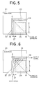
- Fig. 5 is an illustration for explaining a construction of the first embodiment of an L-shaped optical waveguide bending of the present invention
- Fig. 6 is an illustration for explaining a condition of a wave propagating in the L-shaped waveguide bending of Fig. 5.
- An L-shaped optical waveguide bending where the quartz type single mode optical waveguides are angled in L-shaped configuration, will be discussed hereinafter with reference to Figs. 5 and 6.
- the center axes of the incident side single mode waveguide 22 and the output side single mode waveguide 23 extended in the longitudinal directions are intersected at the point O.
- a leaky wave propagation region 24 having the propagation wavelength of the dominant mode of 775 nm corresponding to 1/(2) 1/2 of the single mode waveguides 22 and 23 (effective refractive index is 2.000 corresponding to (2) 1/2 times), and of substantially square-shape having length of one edge of 50 ⁇ m, is provided.
- the leaky wave propagation region 24 is formed by using a spattered region of Ta 2 O 3 .
- These single mode waveguides 22 and 23 and the leaky wave propagation region 24 are set the layer thickness of 2 ⁇ m so that the higher order mode is not generated with respect to the perpendicular direction to the substrate 21 and the number of waves on the thickness direction is mutually consistent with each other.
- the distance 27 between the single mode waveguides 22 and 23 and the leaky wave propagation region 24 is set.
- the energy of the wave launched from the incident end 25 of the incident side single mode waveguide 22 can be efficiently taken out from the output end 26 of the output side single mode waveguide 23.
- Fig. 7 is an illustration for explaining a construction of the second embodiment of a waveguide element according to the present invention
- Fig. 8 is an illustration for explaining a construction of the second embodiment of the waveguide element of Fig. 7.
- the second embodiment of the waveguide element according to the present invention will be discussed hereinafter with reference to Figs. 7 and 8.
- Fig. 7 shows a construction for realizing ideal transmission characteristics using the leaky wave in the waveguide discontinuity, in which two single mode waveguides 32 and 33 having identical cross-sectional structure are arranged to intersect so that the center axes of the two single mode waveguides 32 and 33 extended in the longitudinal directions are interest at an angle ⁇ (0 ⁇ ⁇ ⁇ 90°).
- a substrate 31 is prepared with two single mode waveguides 32 and 33 intersecting the center axes thereof extending in the longitudinal direction at the angle ⁇ (0 ⁇ ⁇ ⁇ 90°), the incident side single mode waveguide 32 having the propagation wavelength of the dominant mode relative to the number of oscillation of the wave is ⁇ G, and the output side single mode waveguide 33 having the same cross-sectional shape and the propagation characteristics.
- a diffraction grating 35 having a period of cos ( ⁇ /2) of the effective propagation wavelength ⁇ G of the single mode waveguides 32 and 33 and a grating vector inclined toward the single mode waveguide 33 for an angle of ⁇ /2 with respect to propagating direction of the wave propagating in the single mode waveguide 32, is formed and the leaky wave propagating region 34 of substantially lozenge shape having one edge length of L.
- These single mode waveguides 32 and 33 and the leaky wave propagating region 34 are set the layer thickness, in which higher order mode is not generated in the substrate 31 in the vertical direction and number of wave of the layer thickness direction is consistent. It should be appreciated that these incident side single mode waveguide 32 and the output side single mode waveguide 33 may be intersect with each other, connected at one point or not intersect. However, it is essential that it is symmetric relative to a straight line OM extending through the point O and equally dividing a supplementary angle ( ⁇ - ⁇ ) of the angle ⁇ . On the other hand, the length contributing for coupling is L.
- the single mode waveguides 32 and 33 and the leaky wave propagation region 34 are set so that a coupling coefficient of amplitude about ⁇ per unit length thereof can be obtained.
- the foregoing waveguide elements are excited by the signal line launched to the incident end 36 of the incident side single mode waveguide 32 to gradually radiate the energy to the leaky wave propagation region 34 with propagation.
- the radiation angle as measured from propagation of the wave is parallel to the grating vector ⁇ G of the diffraction grating 35.
- the total amount of the energy radiated from the incident side single mode waveguide 32 to the leaky wave propagation region 34 is proportional to the following expression with taking the coupling coefficient of the amplitude per unit length being ⁇ : (1 - exp (-2 ⁇ L))/2 ⁇
- the output amount of the energy can be controlled.
- the length of the portion effectively contributing for radiation of energy of the wave in practice is substantially (1/ ⁇ ) from analogizing of the opening of the leaky wave antenna.
- the opening of the antenna per se becomes greater in comparison with the wavelength of the wave sufficiently, radiation directionality of the antenna becomes higher.
- the coupling coefficient ⁇ is sufficiently lowered than (1/ ⁇ G)
- the length L is set to be large so that the total amount of the radiated energy becomes not too small so that the product ⁇ L should not be excessively small.
- the energy of the wave launched from the incident end 15 of the incident side single mode waveguide 32 can be efficiently taken out from the output end 16 of the output side single mode waveguide 33.
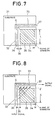
- Fig. 9 is an illustration for explaining a structure of the second embodiment of an L-shaped extremely high frequency wave waveguide bending of the present invention
- Fig. 10 is an illustration for explaining a condition of a wave propagated in the L-shaped extremely high frequency wave waveguide element of Fig. 9.
- Fig. 9 shows an example, in which the second embodiment of the waveguide element according to the present invention is employed in an L-shaped extremely high frequency wave waveguide bending in NRD (Non Radiative Dielectric) guide transmitting an extremely high frequency wave of 50 GHz band.
- NRD Non Radiative Dielectric
- a substrate 41 in which the center axes of an incident side single mode waveguide 42 and a side single mode waveguide 43 respectively extending in the longitudinal direction are interest at a right angle (90°), the incident side single mode waveguide having a propagation wavelength of a dominant mode of 4.243 mm (effective refraction index is 1.414) and a output side single mode waveguide having the same cross-sectional shape and propagation characteristics as the incident side single mode waveguide are provided respectively, is prepared.
- the center axes of the incident side single mode waveguide 42 and the output side single mode waveguide 4 ⁇ 3 extended in the longitudinal directions are intersected at the point O.
- a leaky wave propagation region 44 in which a diffraction grating 45 having a period of 3 mm corresponding to cos ( ⁇ /2) of the effective propagation wavelength ⁇ G of the single mode waveguides 42 and 43 and a grating vector inclined toward the single mode waveguide 43 for an angle of ⁇ /2 with respect to propagating direction of the wave propagating in the single mode waveguide 42, is formed and the leaky wave propagating region 44 of substantially lozenge shape having one edge length of L.
- the layer thickness of single mode waveguides 42 and 43 and the leaky wave propagation region 44 are set to be 2 ⁇ m so that higher order modes will not be generated in respective of substrate in the perpendicular direction to the substrate 41, and the number of wave in the thickness direction, respective, is consistent with each other.
- the distance 48 between the single mode waveguides 42 and 43 and the leaky wave propagation region 44 is set to be 1 mm.
- the energy of the wave launched from the incident end 46 of the incident side single mode waveguide 42 can be efficiently taken out from the output end 47 of the output side single mode waveguide 43.
- Fig. 11 is an illustration for explaining a construction of the third embodiment of a waveguide branch or coupler according to the present invention
- Fig. 12 is an illustration showing a condition of the wave propagating in the waveguide branch or coupler of Fig. 11 as derived derived arithmetically.
- the third embodiment of a waveguide branch or coupler according to the present invention will be discussed hereinafter with reference to Figs. 11 and 12.
- Fig. 11 shows a construction for realizing an ideal transmission characteristics utilizing the leaky wave in a symmetric Y-shaped waveguide branching structure, which is consisted of three single mode waveguides 52, 53 and 54 of mutually identical cross-sectional construction, and, with respect to the center axis of the particular waveguide 52 extended in the longitudinal direction, the center axes of the remaining two waveguides 53 and 54 extended in the longitudinal directions are intersected at an angle ⁇ (0 ⁇ ⁇ ⁇ 90°).
- a substrate 51 having three single mode waveguides 52, 53 and 54, in which the propagation wavelength of the dominant mode with respect to the wave of a certain oscillation frequency is ⁇ G, the cross-sectional shapes and the propagation characteristics are mutually the same, and with respect to the center axis of the particular waveguide 52 extended in the longitudinal direction, the center axes of the remaining two waveguides 53 and 54 extended in the longitudinal directions are intersected at an angle ⁇ (0 ⁇ ⁇ ⁇ 90°), is prepared.
- leaky wave propagation regions 55 and 56 of substantially lozenge shape having one edge length of substantially L with the effective propagation wavelength of the dominant mode being cos ( ⁇ /2) times of the effective propagation wavelength ⁇ G of the single mode waveguides 52 and 53 [or 1/cos ( ⁇ /2) of the effective refractive index nG], are provided.
- These single mode waveguides 52 and 53 and the leaky wave propagation regions 55 and 56 are set at layer thickness respectively so that higher order mode may not be generated with respect to the perpendicular direction of the substrate 51 and number of waves in the layer thickness direction are mutually consistent with each other.
- three single mode waveguides 52, 53 and 54 may be intersect with each other, connected at one point or not intersect. However, it is essential that the single mode waveguides 52 and 53 and the single mode waveguides 52 and 54 respectively extend through the point O and have to be symmetric relative to a straight lines OM, OM' equally dividing a supplementary angle ( ⁇ - ⁇ ) of the angle ⁇ . On the other hand, the length contributing for coupling is L.
- the distances 60 and 61 between the single mode waveguides 52, 53 and 54 and the leaky wave propagation regions 55 and 56 are adjusted to obtain the coupling coefficient of the amplitude of about ⁇ .
- control means similar to that explained in the first embodiment of the present invention may be employed.
- the Y-shaped waveguide branch or coupler shown in Fig. 11 is excited by the signal light launched to the incident end 57 of the single mode waveguide 52 with gradually radiating to the leaky wave propagation regions 55 and 56.
- the principle of the coupling of the wave via the leaky wave is the same as that discussed in terms of the first embodiment, except for the region contributing varied from one into two.
- the energy of the wave launched from the incident end 57 of the incident side single mode waveguide 52 can be efficiently taken out from the output ends 58 and 59 of respective of the output side single mode waveguides 53 and 54.
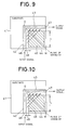
- Fig. 13 is an illustration for explaining a construction of the third embodiment of a T-shaped waveguide branch or coupler according to the present invention
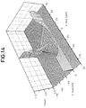
- Fig. 14 is an illustration showing a condition of the wave propagating in the T-shaped waveguide branch or coupler of Fig. 13 as derived arithmetically.
- the third embodiment of the T-shaped waveguide branch or coupler according to the present invention will be discussed hereinafter with reference to Figs. 13 and 14.
- Fig. 13 shows an example employing the T-shaped waveguide type optical branch or coupler of the quartz type single mode optical waveguide of the shaft of the third embodiment of the present invention set forth above
- Fig. 14 shows a result of theoretical calculation of the amplitude of the wave to be propagated in the T-shaped waveguide type optical branch or coupler.
- a substrate 71 in which the center axes of single mode waveguides 72, 73 and 74 extending in the longitudinal direction are intersected at a right angle (90°), the incident side single mode waveguide 72 having a propagation wavelength of a dominant mode of 1096 nm (effective refractive index is 1.414) and a output side single mode waveguides 73 and 74 having the same cross-sectional shape and propagation characteristics as the incident side single mode waveguide are provided respectively, is prepared.
- the side single mode waveguides 73 and 74 extended in the longitudinal directions are symmetric relative to each other.
- a leaky wave propagation regions 75 and 76 having the propagation wavelength of the dominant mode of 775 nm corresponding to 1/(2) 1/2 of respective effective propagation wavelength ⁇ G of the single mode waveguides 72, 73 and 74 (effective refraction index is 2.000 corresponding to (2) 1/2 times), and of substantially square-shape having length of one edge of 50 ⁇ m, are provided.
- the leaky wave propagation regions 75 and 76 are formed by using a spattered region of Ta 2 O 3 .
- These single mode waveguides 72, 73 and 74 and the leaky wave propagation regions 75 and 76 are set such a layer thickness so that the higher order mode is not generated with respect to the perpendicular direction to the substrate 71 and the number of waves on the thickness direction is mutually consistent with each other.
- three single mode waveguides 72, 73 and 74 may be intersect with each other, connected at one point or not intersect. However, it is essential that the single mode waveguides 72 and 73 and the single mode waveguides 72 and 74 respectively extend through the point O and have to be symmetric relative to a straight lines OM, OM' equally dividing a supplementary angle ( ⁇ - ⁇ ) of the angle ⁇ .
- the distances 80 and 81 between the single mode waveguides 72, 73 and 74 and the leaky wave propagation regions 75 and 76 are set.
- the energy of the wave launched from the incident end 77 of the incident side single mode waveguide 72 can be efficiently taken out from the output ends 78 and 79 of the output side single mode waveguides 73 and 74.
- Fig. 15 is an illustration showing a construction of the fourth embodiment of a waveguide element according to the present invention.
- the fourth embodiment of the waveguide element according to the present invention has the same construction as the waveguide element set forth above except that the single mode waveguides 91 and 92 are connected with each other by a bending waveguide 93 having a predetermined radius of curvature.
- the curvature radius of the bending waveguide 93 is variable depending upon connecting condition.
- the shape of the leaky wave propagation region 94 is varied depending upon variation of the curvature radius of the bending waveguide 93.
- the reference numeral 95 denotes an incident end of the incident side single mode waveguide 91
- 96 denotes an output end of the output side single mode waveguide 92
- the reference numeral 97 denotes the interval between the single mode waveguide 91, 92 and the leaky wave propagation region 94.
- Fig. 16 is an illustration showing a construction of the fifth embodiment of a waveguide element according to the present invention.
- the fifth embodiment of the waveguide element according to the present invention has the same construction as the waveguide element set forth above except that taper portions 104 and 105 are provided.
- the taper portions 104 and 105 are designed for continuously varying a distance 108 along the longitudinal direction of the single mode waveguides 101 and 102 for spatially controlling a radiation amount and a radiation pattern of the wave to a leaky wave propagation region 103.
- the coupling coefficient ⁇ is desired to be greater, it becomes possible to avoid a concern for reflection at a moment where the wave reaches the portion starting coupling of between the single mode waveguides 101 and 102 and the leaky wave propagation region 103.
- the shape of the leaky wave propagation region 103 is not complete lozenge shape but is slightly deformed.
- the reference numeral 106 denotes an incident end of the incident side single mode waveguide 101
- 107 denotes an output end of the output side single move waveguide 102.
- the foregoing content will be applicable for the waveguide type branch or coupler.
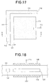
- Fig. 17 is an illustration showing a construction of the sixth embodiment of a waveguide element according to the present invention
- Fig. 18 is a section taken along line A - A of Fig. 17.
- the shown embodiment of the waveguide element according to the present invention has the same construction as the foregoing waveguide element except that a mechanism for controlling the leaky wave propagation region 113 is provided.
- a mechanism for controlling the leaky wave propagation region 113 is constructed with a terminal 114, to which a voltage (electric field) as a control signal is applied, electrodes 118 and 119 and an electro-optic crystal 120.
- a voltage electric field
- electrodes 118 and 119 and an electro-optic crystal 120.
- the electro-optic crystal 120 a material (e.g. lithium niobate and the like) variable of absorption coefficient or refraction index depending upon the electric field, may be used.
- the absorption coefficient and/or refraction index of the electro-optic crystal 120 are varied by the electrodes 118 and 119.
- one of the effective propagation wavelength and attenuation coefficient of wave to be propagated in the leaky wave propagation region 113 can be controlled.
- the reference numeral 115 denotes an incident end of the incident side single mode waveguide 111
- 116 denotes a output end of the output side single mode waveguide 112
- 117 denotes distance between the single mode waveguides 111 and 112 and the leaky wave propagation region 113
- the reference numeral 121 denotes a quartz forming respective of the single mode waveguides 111 and 112 and the leaky wave propagation region 113
- 112 denotes a core for forming the single mode waveguide 111.
- the length of the taper portion provided for the purpose of transition at upstream and downstream sides of the waveguide discontinuity can be eliminated, a propagation loss proportional to the length can be reduced. Also, since excessive loss due to radiation and/or reflection at the discontinuity portion may not be caused, loss of energy of the wave in the waveguide discontinuity can be reduced.
- the waveguide functional elements can be connected with quite low loss, package density of the waveguide integrated circuit can be improved.
- the waveguide element, the waveguide branch or coupler element, the waveguide integrated circuit according to the present invention may provide means for acutely varying the wave propagation direction in short distance to realize improvement of freedom of layout of various waveguide functional elements, down-sizing, reduction of low, improvement of package density and so forth.
- acute waveguide discontinuity such as a right angle bending (L-shaped bending) or branching (T-shaped branching) can be realized by leaky wave coupling of the wave propagating in the first and second straight waveguides forming at least one of bending and intersection substantially at the same rate, by means of leaky wave propagation region.
- the waveguide branch or coupler element in the waveguide branch or coupler element having at least one of bending and intersection of the straight waveguides for propagating the wave, acute waveguide discontinuity, such as a right angle bending (L-shaped bending) or branching (T-shaped branching) can be realized by leaky wave coupling of the wave propagating in the first and second straight waveguides forming at least one of bending and intersection substantially at the same rate, by means of the first leaky wave propagation region, and by leaky wave coupling of the wave propagating in the first and third straight waveguides forming at least one of bending and intersection substantially at the same rate, by means of the second leaky wave propagation region.
- acute waveguide discontinuity such as a right angle bending (L-shaped bending) or branching (T-shaped branching)
- L-shaped bending right angle bending
- T-shaped branching branching
- the waveguide integrated circuit according to the present invention constructed as set forth above, in the waveguide integrated circuit having at least one of bending and intersection of the straight waveguides for propagating the wave, acute waveguide discontinuity, such as a right angle bending (L-shaped bending) or branching (T-shaped branching) can be realized by leaky wave coupling of the wave propagating in the first and second straight waveguides forming at least one of bending and intersection substantially at the same rate, by means of leaky wave propagation region.
- acute waveguide discontinuity such as a right angle bending (L-shaped bending) or branching (T-shaped branching) can be realized by leaky wave coupling of the wave propagating in the first and second straight waveguides forming at least one of bending and intersection substantially at the same rate, by means of leaky wave propagation region.
Landscapes
- Physics & Mathematics (AREA)
- Nonlinear Science (AREA)
- General Physics & Mathematics (AREA)
- Optics & Photonics (AREA)
- Engineering & Computer Science (AREA)
- Microelectronics & Electronic Packaging (AREA)
- Optical Integrated Circuits (AREA)
Applications Claiming Priority (3)
| Application Number | Priority Date | Filing Date | Title |
|---|---|---|---|
| JP13020997 | 1997-05-21 | ||
| JP130209/97 | 1997-05-21 | ||
| JP13020997A JP3233067B2 (ja) | 1997-05-21 | 1997-05-21 | 導波路素子及び導波路型合分波素子並びに導波路集積回路 |
Publications (2)
| Publication Number | Publication Date |
|---|---|
| EP0880037A2 true EP0880037A2 (de) | 1998-11-25 |
| EP0880037A3 EP0880037A3 (de) | 2000-08-02 |
Family
ID=15028706
Family Applications (1)
| Application Number | Title | Priority Date | Filing Date |
|---|---|---|---|
| EP98109118A Withdrawn EP0880037A3 (de) | 1997-05-21 | 1998-05-19 | Wellenleiterelement, Wellenleiterverzweigung oder Kopplerelement und integrierter Wellenleiterschaltkreis |
Country Status (4)
| Country | Link |
|---|---|
| US (1) | US6335994B1 (de) |
| EP (1) | EP0880037A3 (de) |
| JP (1) | JP3233067B2 (de) |
| CA (1) | CA2238232C (de) |
Families Citing this family (11)
| Publication number | Priority date | Publication date | Assignee | Title |
|---|---|---|---|---|
| US6381380B1 (en) | 1998-06-24 | 2002-04-30 | The Trustees Of Princeton University | Twin waveguide based design for photonic integrated circuits |
| US6795622B2 (en) * | 1998-06-24 | 2004-09-21 | The Trustess Of Princeton University | Photonic integrated circuits |
| US6885781B2 (en) * | 2002-05-03 | 2005-04-26 | Fujitsu Limited | Thin film electro-optical deflector device and a method of fabrication of such a device |
| US7035508B2 (en) * | 2003-04-18 | 2006-04-25 | Metrophotonics Inc. | Waveguide structure having improved reflective mirror features |
| US7079716B2 (en) * | 2003-06-26 | 2006-07-18 | Bae Systems Information And Electronic Systems Integration Inc. | Integrated photonic circuits with vertical connections |
| US7230963B2 (en) * | 2004-04-14 | 2007-06-12 | The Trustees Of Princeton University | Monolithic wavelength stabilized asymmetric laser |
| US7447397B1 (en) | 2004-06-14 | 2008-11-04 | Dynamic Method Enterprises Limited | Optical switch matrix |
| US7333689B2 (en) * | 2005-09-30 | 2008-02-19 | The Trustees Of Princeton University | Photonic integrated devices having reduced absorption loss |
| US7343061B2 (en) * | 2005-11-15 | 2008-03-11 | The Trustees Of Princeton University | Integrated photonic amplifier and detector |
| US7826693B2 (en) | 2006-10-26 | 2010-11-02 | The Trustees Of Princeton University | Monolithically integrated reconfigurable optical add-drop multiplexer |
| US11994725B2 (en) * | 2020-11-03 | 2024-05-28 | Amrita Vishwa Vidyapectham | Circular optical array system using waveguide fed angled mirrors |
Family Cites Families (17)
| Publication number | Priority date | Publication date | Assignee | Title |
|---|---|---|---|---|
| US3753157A (en) * | 1971-06-30 | 1973-08-14 | Ibm | Leaky wave couplers for guided elastic wave and guided optical wave devices |
| GB1525492A (en) * | 1974-09-20 | 1978-09-20 | Max Planck Gesellschaft | Self imaging system using a waveguide |
| US4185884A (en) * | 1977-12-20 | 1980-01-29 | Sperry Corporation | Four port optical internal reflectance switchable coupler |
| JPS609604B2 (ja) | 1980-07-05 | 1985-03-12 | 栄一 溜渕 | 道路の伸縮継手構造 |
| JPS6262304A (ja) | 1985-09-13 | 1987-03-19 | Omron Tateisi Electronics Co | Y分岐光導波路装置 |
| US4749248A (en) * | 1985-11-06 | 1988-06-07 | American Telephone And Telegraph Company At&T Bell Laboratories | Device for tapping radiation from, or injecting radiation into, single made optical fiber, and communication system comprising same |
| JPS62258407A (ja) | 1986-05-01 | 1987-11-10 | Sumitomo Electric Ind Ltd | 光分岐結合器 |
| JPH06100694B2 (ja) | 1986-07-14 | 1994-12-12 | 富士通株式会社 | 光導波路の形成方法 |
| JPS63217330A (ja) | 1987-03-06 | 1988-09-09 | Hitachi Ltd | 光スイツチ |
| US4810049A (en) * | 1987-04-02 | 1989-03-07 | American Telephone And Telegraph Company, At&T Bell Laboratories | Reducing bend and coupling losses in integrated optical waveguides |
| JP2553583B2 (ja) | 1987-09-02 | 1996-11-13 | 三菱電機株式会社 | 光集積回路用折曲り導波路 |
| EP0347233A3 (de) * | 1988-06-16 | 1991-02-13 | Gec-Marconi Limited | Anordnung integrierter Optik |
| EP0365724A1 (de) * | 1988-10-26 | 1990-05-02 | THE GENERAL ELECTRIC COMPANY, p.l.c. | Integrierte optische Wellenleiterkrümmung |
| JPH05173030A (ja) | 1991-12-20 | 1993-07-13 | Nec Eng Ltd | 光導波路の曲がり構造 |
| DE4208658A1 (de) * | 1992-03-18 | 1993-09-23 | Manfred Prof Dr Boerner | Dielektrischer einmoden-lichtwellenleiter mit richtungsumlenkung auf engstem raum zum einsatz in integriert optischen schaltungen |
| US5349602A (en) * | 1993-03-15 | 1994-09-20 | Sdl, Inc. | Broad-area MOPA device with leaky waveguide beam expander |
| JP5719402B2 (ja) | 2012-07-09 | 2015-05-20 | 本田技研工業株式会社 | 内燃機関の燃料噴射制御装置 |
-
1997
- 1997-05-21 JP JP13020997A patent/JP3233067B2/ja not_active Expired - Fee Related
-
1998
- 1998-05-19 EP EP98109118A patent/EP0880037A3/de not_active Withdrawn
- 1998-05-20 CA CA002238232A patent/CA2238232C/en not_active Expired - Fee Related
- 1998-05-21 US US09/082,799 patent/US6335994B1/en not_active Expired - Fee Related
Also Published As
| Publication number | Publication date |
|---|---|
| US6335994B1 (en) | 2002-01-01 |
| CA2238232C (en) | 2002-01-08 |
| CA2238232A1 (en) | 1998-11-21 |
| JP3233067B2 (ja) | 2001-11-26 |
| JPH10319260A (ja) | 1998-12-04 |
| EP0880037A3 (de) | 2000-08-02 |
Similar Documents
| Publication | Publication Date | Title |
|---|---|---|
| US9588292B2 (en) | Integrated photonic devices based on waveguides patterned with optical antenna arrays | |
| US5838844A (en) | Integrated optical circuit comprising a polarization convertor | |
| US7142165B2 (en) | Waveguide and slotted antenna array with moveable rows of spaced posts | |
| US5526449A (en) | Optoelectronic integrated circuits and method of fabricating and reducing losses using same | |
| US8026854B2 (en) | Stripline-type composite right/left-handed transmission line or left-handed transmission line, and antenna that uses same | |
| US20030059147A1 (en) | Optical waveguide structures | |
| US4130342A (en) | Passive optical channel crossover, switch and bend structure | |
| US20040008943A1 (en) | Optical waveguide structures | |
| US20020131667A1 (en) | Optical waveguide structures | |
| US6335994B1 (en) | Waveguide element, waveguide branch or coupler element and waveguide intergrated circuit | |
| JPS63500838A (ja) | 複式誘電体多心伝送回線とその応用装置 | |
| US5661825A (en) | Integrated optical circuit comprising a polarization convertor | |
| US20080180340A1 (en) | Waveguide Coupling Devices | |
| CN115792954A (zh) | 一种光学相控阵、激光雷达发射模块以及激光雷达 | |
| EP1369741B1 (de) | Resonanter elekro-optischer Modulator zur Erzeugung kurzer optischer Pulse | |
| JP5071859B2 (ja) | 右手/左手系複合導波管およびその製造方法 | |
| Khodadadi et al. | Theoretical analysis of a super-mode waveguide and design of a complementary triangular hybrid plasmonic nano-antenna | |
| CN110661069B (zh) | 一种等离子体波导结构以及漏波天线 | |
| Izutsu et al. | Broad‐band guided‐wave light intensity modulator | |
| US5528717A (en) | Hybrid dielectric slab beam waveguide | |
| WO1986003891A2 (en) | A compound dielectric multi-conductor transmission line and devices constructed therefrom | |
| Chen et al. | Wide-angle frequency scanning metasurface antenna fed by spoof plasmonic waveguide | |
| JPH06308437A (ja) | 光制御素子 | |
| Zafari et al. | Engineering Leaky Wave Antennas: Modulated Impedance Surfaces and Radiative Characteristics | |
| JP2022117842A (ja) | トポロジカル垂直結合器 |
Legal Events
| Date | Code | Title | Description |
|---|---|---|---|
| PUAI | Public reference made under article 153(3) epc to a published international application that has entered the european phase |
Free format text: ORIGINAL CODE: 0009012 |
|
| AK | Designated contracting states |
Kind code of ref document: A2 Designated state(s): DE FR GB NL SE |
|
| AX | Request for extension of the european patent |
Free format text: AL;LT;LV;MK;RO;SI |
|
| PUAL | Search report despatched |
Free format text: ORIGINAL CODE: 0009013 |
|
| AK | Designated contracting states |
Kind code of ref document: A3 Designated state(s): AT BE CH CY DE DK ES FI FR GB GR IE IT LI LU MC NL PT SE |
|
| AX | Request for extension of the european patent |
Free format text: AL;LT;LV;MK;RO;SI |
|
| 17P | Request for examination filed |
Effective date: 20000626 |
|
| AKX | Designation fees paid |
Free format text: DE FR GB NL SE |
|
| 17Q | First examination report despatched |
Effective date: 20050113 |
|
| STAA | Information on the status of an ep patent application or granted ep patent |
Free format text: STATUS: THE APPLICATION HAS BEEN WITHDRAWN |
|
| 18W | Application withdrawn |
Effective date: 20050426 |