EP0880048A1 - Modulateurs acousto-optiques comprenant des guides d'ondes planaires - Google Patents
Modulateurs acousto-optiques comprenant des guides d'ondes planaires Download PDFInfo
- Publication number
- EP0880048A1 EP0880048A1 EP98303702A EP98303702A EP0880048A1 EP 0880048 A1 EP0880048 A1 EP 0880048A1 EP 98303702 A EP98303702 A EP 98303702A EP 98303702 A EP98303702 A EP 98303702A EP 0880048 A1 EP0880048 A1 EP 0880048A1
- Authority
- EP
- European Patent Office
- Prior art keywords
- waveguide
- multimode
- section
- modulator
- optical signal
- Prior art date
- Legal status (The legal status is an assumption and is not a legal conclusion. Google has not performed a legal analysis and makes no representation as to the accuracy of the status listed.)
- Granted
Links
- 230000003287 optical effect Effects 0.000 claims abstract description 123
- 230000005540 biological transmission Effects 0.000 claims abstract description 114
- 238000010897 surface acoustic wave method Methods 0.000 claims abstract description 81
- 230000001902 propagating effect Effects 0.000 claims abstract description 59
- 230000008878 coupling Effects 0.000 claims abstract description 36
- 238000010168 coupling process Methods 0.000 claims abstract description 36
- 238000005859 coupling reaction Methods 0.000 claims abstract description 36
- 238000012546 transfer Methods 0.000 claims abstract description 14
- VYPSYNLAJGMNEJ-UHFFFAOYSA-N Silicium dioxide Chemical compound O=[Si]=O VYPSYNLAJGMNEJ-UHFFFAOYSA-N 0.000 claims description 76
- 239000000377 silicon dioxide Substances 0.000 claims description 22
- 239000013307 optical fiber Substances 0.000 claims description 17
- 238000000926 separation method Methods 0.000 claims description 11
- 239000011358 absorbing material Substances 0.000 claims description 9
- 230000007704 transition Effects 0.000 claims description 4
- 239000004593 Epoxy Substances 0.000 claims description 3
- 230000008859 change Effects 0.000 abstract description 14
- 230000000737 periodic effect Effects 0.000 abstract description 13
- 230000003993 interaction Effects 0.000 description 25
- 239000000758 substrate Substances 0.000 description 13
- 239000010410 layer Substances 0.000 description 10
- 238000005253 cladding Methods 0.000 description 9
- 230000002238 attenuated effect Effects 0.000 description 6
- XUIMIQQOPSSXEZ-UHFFFAOYSA-N Silicon Chemical compound [Si] XUIMIQQOPSSXEZ-UHFFFAOYSA-N 0.000 description 5
- 239000000463 material Substances 0.000 description 5
- 229910052710 silicon Inorganic materials 0.000 description 5
- 239000010703 silicon Substances 0.000 description 5
- 239000012792 core layer Substances 0.000 description 4
- 239000000835 fiber Substances 0.000 description 4
- 239000011521 glass Substances 0.000 description 4
- 230000014509 gene expression Effects 0.000 description 3
- 238000004519 manufacturing process Methods 0.000 description 3
- 238000000034 method Methods 0.000 description 3
- 238000012545 processing Methods 0.000 description 3
- 230000000644 propagated effect Effects 0.000 description 3
- 230000005855 radiation Effects 0.000 description 3
- 230000001419 dependent effect Effects 0.000 description 2
- 238000012986 modification Methods 0.000 description 2
- 230000004048 modification Effects 0.000 description 2
- 238000004806 packaging method and process Methods 0.000 description 2
- 239000002245 particle Substances 0.000 description 2
- 235000003913 Coccoloba uvifera Nutrition 0.000 description 1
- 229910001218 Gallium arsenide Inorganic materials 0.000 description 1
- 240000008976 Pterocarpus marsupium Species 0.000 description 1
- 239000000853 adhesive Substances 0.000 description 1
- 230000001070 adhesive effect Effects 0.000 description 1
- 230000015556 catabolic process Effects 0.000 description 1
- 239000000919 ceramic Substances 0.000 description 1
- 238000005234 chemical deposition Methods 0.000 description 1
- 238000004891 communication Methods 0.000 description 1
- 238000007796 conventional method Methods 0.000 description 1
- 238000006731 degradation reaction Methods 0.000 description 1
- 238000000151 deposition Methods 0.000 description 1
- 230000008021 deposition Effects 0.000 description 1
- 238000013461 design Methods 0.000 description 1
- 238000009826 distribution Methods 0.000 description 1
- 230000000694 effects Effects 0.000 description 1
- 238000005530 etching Methods 0.000 description 1
- 239000005350 fused silica glass Substances 0.000 description 1
- 230000007062 hydrolysis Effects 0.000 description 1
- 238000006460 hydrolysis reaction Methods 0.000 description 1
- 230000010354 integration Effects 0.000 description 1
- 238000001459 lithography Methods 0.000 description 1
- 229920001296 polysiloxane Polymers 0.000 description 1
- 230000008569 process Effects 0.000 description 1
- 239000011343 solid material Substances 0.000 description 1
Images


Classifications
-
- G—PHYSICS
- G02—OPTICS
- G02F—OPTICAL DEVICES OR ARRANGEMENTS FOR THE CONTROL OF LIGHT BY MODIFICATION OF THE OPTICAL PROPERTIES OF THE MEDIA OF THE ELEMENTS INVOLVED THEREIN; NON-LINEAR OPTICS; FREQUENCY-CHANGING OF LIGHT; OPTICAL LOGIC ELEMENTS; OPTICAL ANALOGUE/DIGITAL CONVERTERS
- G02F1/00—Devices or arrangements for the control of the intensity, colour, phase, polarisation or direction of light arriving from an independent light source, e.g. switching, gating or modulating; Non-linear optics
- G02F1/29—Devices or arrangements for the control of the intensity, colour, phase, polarisation or direction of light arriving from an independent light source, e.g. switching, gating or modulating; Non-linear optics for the control of the position or the direction of light beams, i.e. deflection
- G02F1/33—Acousto-optical deflection devices
- G02F1/335—Acousto-optical deflection devices having an optical waveguide structure
-
- G—PHYSICS
- G02—OPTICS
- G02F—OPTICAL DEVICES OR ARRANGEMENTS FOR THE CONTROL OF LIGHT BY MODIFICATION OF THE OPTICAL PROPERTIES OF THE MEDIA OF THE ELEMENTS INVOLVED THEREIN; NON-LINEAR OPTICS; FREQUENCY-CHANGING OF LIGHT; OPTICAL LOGIC ELEMENTS; OPTICAL ANALOGUE/DIGITAL CONVERTERS
- G02F1/00—Devices or arrangements for the control of the intensity, colour, phase, polarisation or direction of light arriving from an independent light source, e.g. switching, gating or modulating; Non-linear optics
- G02F1/01—Devices or arrangements for the control of the intensity, colour, phase, polarisation or direction of light arriving from an independent light source, e.g. switching, gating or modulating; Non-linear optics for the control of the intensity, phase, polarisation or colour
- G02F1/11—Devices or arrangements for the control of the intensity, colour, phase, polarisation or direction of light arriving from an independent light source, e.g. switching, gating or modulating; Non-linear optics for the control of the intensity, phase, polarisation or colour based on acousto-optical elements, e.g. using variable diffraction by sound or like mechanical waves
- G02F1/125—Devices or arrangements for the control of the intensity, colour, phase, polarisation or direction of light arriving from an independent light source, e.g. switching, gating or modulating; Non-linear optics for the control of the intensity, phase, polarisation or colour based on acousto-optical elements, e.g. using variable diffraction by sound or like mechanical waves in an optical waveguide structure
Definitions
- the invention relates to optical signal modulators.
- Optical transmission and processing systems are being implemented for use in various communication applications.
- telephone and data transmission systems are now in use that utilize optical fibers to transmit voice and data signals over long distances.
- data and/or digitized voice signals are modulated with an optical carrier signal for transmission.
- Modulation is the variation of a characteristic of a signal wave in accordance with a characteristic of another signal wave.
- a modulator arrangement includes an acoustic transducer formed on a top surface of a glass substrate.
- a bottom surface of the substrate has a precision-formed groove with an exact radius. This groove radius is precisely formed to provide a Hertzian contact between an optical fiber and the substrate groove, when the fiber is pressed into the groove.
- a Hertzian contact enables propagation of acoustic waves over an acoustic path formed entirely of solid material from the substrate through the Hertzian contact interface and into the waveguide.
- acoustic waves generated by the transducer propagate into the substrate, through the formed Hertzian contact, and into the optical fiber. These acoustic waves then interact and modulate an optical signal propagating in a transmission mode within a core of the optical fiber by coupling signal power from this core transmission mode to a transmission mode of the lossy cladding layer surrounding the core of the optical fiber.
- Optical planar waveguide structures such as silica optical circuits
- Optical planar waveguide structures are substantially more compact than fiber-based modulators and are manufacturable at relatively low cost.
- the basic structure of such devices is described in C. H. Henry et al., "Glass Waveguides on Silicon for Hybrid Optical Packaging", 7 J. Lightwave Technol., pp. 1530-1539 (1989).
- Typical silica optical circuits have core waveguide structures of doped silica glass disposed within silica glass formed on a substrate and enable multiple optical components to be formed on a common substrate.
- planar waveguides lack the existence of discrete cladding transmission modes that are typically relied upon to produce fiber-based modulators.
- the acousto-optic configuration employed in fiber-based modulators is inapplicable to planar waveguide structures. Accordingly, a need exists for a planar waveguide modulator configuration.
- the invention is directed to an optical planar waveguide modulator circuit employing an acousto-optic effect to modulate a light signal propagating through the waveguide.
- the modulator employs a waveguide structure having an input section connected to a multimode section connected to an output section.
- the input and output sections have structures for propagating an optical signal in a common first, even transmission mode.
- the multimode section has a structure in which an optical signal can propagate in the first transmission mode as well as a second, next higher order, odd transmission mode that is not supported by the input and output sections.
- the waveguide structure enables propagation of an optical signal from the input section through the multimode section to the output section substantially in the even transmission mode.
- a surface acoustic wave (SAW) source is employed to produce a surface acoustic wave or Rayleigh wave capable of providing sufficient acoustic wave energy to the buried multimode waveguide section to cause a sufficient periodic change in the refractive index to couple light energy between the even and odd transmission modes.
- SAW surface acoustic wave
- a portion of power of an optical signal propagating in an even transmission mode is transferred to the odd transmission mode due to the periodic refractive index change caused by the surface acoustic wave.
- This power transfer causes an attenuation of the corresponding signal propagating in the even transmission mode. Since the odd transmission mode is not supported by the output section, the signal propagating from the multimode section to the output section is substantially in the even transmission mode which is the attenuated optical signal.
- the extent of power transfer, and correspondingly the extent of attenuation of the optical signal propagating through the multimode section in the even transmission mode, is based on the intensity of the generated surface acoustic wave.
- Further embodiments employ such coupling of the transmission modes of a multimode waveguide for modulating an optical signal propagating in a single mode waveguide having a transmission mode evanescent field coupled to the even transmission mode of the multimode waveguide.
- the invention relies on surface acoustic waves for providing sufficient acoustic wave energy to a multimode planar waveguide for causing a desirable periodic change in its refractive index to couple power of an optical signal propagating in a first, even transmission mode of the waveguide to a second, next higher order, odd transmission mode of the waveguide.
- Such coupling is advantageously used in the invention to attenuate an optical signal propagating in the even transmission mode by transferring power to the odd transmission mode by directing a surface acoustic wave at the multimode waveguide.
- the extent of the attenuation is dependent on the magnitude of the power of the surface acoustic wave interacting with the waveguide. Accordingly, it is possible to modulate an optical signal with a second signal by varying the surface acoustic wave power in accordance with the varying magnitude of the second signal.
- such a multimode waveguide is connected between single mode input and output planar waveguide sections to enable propagation of an optical signal from the input section through the multimode section to the output section substantially in the first, even transmission mode.
- a surface acoustic wave propagating through the multimode section causes a sufficient periodic change in the refractive index to couple light energy between the first and second transmission modes.
- a portion of power of an optical signal propagating in the even transmission mode is transferred to the next higher order, odd transmission mode due to the induced periodic refractive index change. This power transfer causes an attenuation of the corresponding signal propagating in the even transmission mode.
- the signal propagating from the multimode region to the output single mode section is substantially the attenuated optical signal propagating in the even transmission mode. Moreover, since the extent of the attenuation of the optical signal propagating in the even transmission mode is based on the power of the surface acoustic wave, it is possible to modulate an optical signal with a second signal by varying the surface acoustic wave power based on this second signal.
- a surface acoustic wave also referred to as a Rayleigh wave, is a particular type of acoustic wave that is guided along a plane surface of a material with its amplitude decaying exponentially with depth into the material.
- An acoustic wave is an elastic non-electromagnetic wave having a frequency typically in the range from below one hertz up to tens of gigahertz.
- An acoustic wave can be propagated in a medium having inertia and elasticity (the existence of forces which tend to restore any part of a medium to its original position), and in which displaced particles transfer momentum to adjoining particles and are themselves restored to their original position.
- silica optical circuit structures include optical waveguides formed relatively near a plane surface of the structures and since 90% of the energy of a surface acoustic wave propagates within one acoustical wavelength of the plane surface, it is possible to select a surface acoustic wave wavelength that enables the use of a multimode waveguide section of advantageously short length for providing the optical signal modulation of the invention.
- Numerous silica optical modulator configurations are useable for performing optical signal modulation according to the invention.
- FIG. 1 depicts an exemplary modulator 1 in accordance with s first embodiment of the invention.
- the modulator 1 includes a surface acoustic wave (SAW) source 5 positioned on a surface 11 of a silica optical structure 10 containing an exemplary planar modulator waveguide structure 15.
- the planar waveguide 15 is located within silica glass 20 formed on a substrate 25 of the silica optical structure 10.
- the SAW source 5 is positioned relative to the waveguide structure such that generated surface acoustic waves interact with the waveguide structure 15 at a particular phase matching angle relative to a multimode section of the waveguide structure 15 producing the desired coupling of transmission modes of the multimode section as described in greater detail below with regard to FIG. 2.
- An exemplary fabrication process for the silica optical structure 10 is as follows: a base layer of silica glass is deposited on the substrate 25, such as a silicon substrate using, for example, low pressure vapor chemical deposition or flame hydrolysis; and then a thin core layer of doped silica glass is deposited on this silica glass layer; the core layer is then configured to the desired structure of the waveguide 15 using standard photo-lithographic techniques, such as lithography, etching; and a layer of doped silica glass is then optionally deposited over the core layer to act as a top cladding.
- a suitable doping profile for the doped silica glass is uniform step-index distribution. While the proceeding description relates to silica on silicon waveguide devices, it should be understood that it is possible to fabricate the circuit on other substrate materials including fused quartz, ceramic or III-V materials, such as InP or GaAs.
- the silica glass top cladding and the base layer of silica glass form the silica glass 20.
- Suitable thicknesses for the base silica layer, core layer and top cladding layer are 10 to 20 ⁇ m, 4 to 8 ⁇ m and 0 to 20 ⁇ m, respectively. Thicknesses less than 10 ⁇ m for the base silica layer are undesirable because of light loss to the substrate while thickness greater than 20 ⁇ m are generally disadvantageous because of long deposition times required to form such thicknesses.
- SAW source 5 in producing surface acoustic waves in the silica optical structure 10 is not critical to practicing the invention.
- Exemplary devices for the SAW source 5 include conventional interdigital transducers and other ZnO transducer configurations which are described in, for example, the previously cited Surface-Wave Device reference.
- FIG. 2 A top view of the planar waveguide structure 15 in the silica optical structure 10 is shown in FIG. 2.
- the source 5 and optional damper 30 of FIG. 1 have not been shown in FIG. 2 for ease of illustration.
- the planar waveguide structure 15 includes an input section 100, a multimode section 105, and an output section 110.
- the input and output sections 100 and 110 are single mode sections capable of propagating an optical signal in a common even transmission mode.
- the multimode section 105 can propagate an optical signal in this even transmission mode as well as in a next higher, odd transmission mode.
- Phase fronts of a surface acoustic wave generated by the SAW source 5 of FIG. 1 are represented by reference number 125 and are at a particular phase matching angle ⁇ relative to the multimode section 105 in order to provide a particular condition of a periodic refractive index change in the multimode section 105.
- phase matching achieves the desired coupling of power of optical signals between the even and odd transmission modes.
- the multimode section 105 has an interaction length L over which a surface acoustic wave provides such condition.
- the number of transmission modes a waveguide section can propagate is determinable from the waveguide's normalized frequency parameter which is commonly referred to as the V -number of the section.
- the V -number is based on the signal wavelength to be propagated, cross-sectional area of the waveguide section and the relative refractive index difference between the waveguide section and the surrounding silica glass.
- a common expression for determining the V-number follows and is described in greater detail in D. Marcuse, Light Transmission Optics, ch. 8, p. 327 (Van Nostrand Reinhold Co., N.Y., 1992), which is incorporated by reference herein.
- V 2 ⁇ ⁇ a n 2 1 - n 2 2 , where ⁇ is the wavelength of an optical signal, the value a is the width of the particular waveguide section and the values n 1 and n 2 are the refractive indexes of the previously described core and cladding layers, respectively.
- Exemplary refractive index values for the silica core and cladding layers n 1 and n 2 are 1.48 and 1.46, respectively.
- a particular cross-sectional area of the multimode waveguide section 105 and/or the relative refractive index difference between the waveguide section 105 and the surrounding silica glass 20 is employed such that the section 105 can propagate optical signals in a first, even transmission mode as well as a second, next higher odd transmission mode.
- the particular cross-sectional area of the waveguide 15 and the relative refractive index difference between the waveguide 15 and/or the surrounding silica glass 20 is employed for the input and output waveguide sections 100 and 110 such that they are capable of propagating an optical signal over a broad bandwidth in an even transmission mode.
- the particular cross-sectional areas and/or the relative refractive index differences are chosen for the output waveguide section 110 to enable power of an optical signal propagating substantially in the even transmission mode to enter the output waveguide section 110 and power of the optical signal propagating substantially in the odd transmission mode to not enter the section 110.
- Such optical signal power propagating in the odd transmission mode of the multimode section 105 is dissipated as radiation.
- exemplary single mode waveguide structures for the waveguide sections 100 and 110 having widths W I and W O of approximately 5 ⁇ m and a height in the range of 4 ⁇ m to 8 ⁇ m as well as a common refractive index n 1 that is in excess of 0.64% of the refractive index n 2 of the surrounding silica glass 20 can propagate optical signals having wavelengths in the range of, for example, 1.25 ⁇ m to 1.6 ⁇ m in even (symmetrical) or odd (asymmetrical) transmission modes.
- an exemplary multimode structure for the waveguide section 105 having a width in the range of 17.0 ⁇ m and a height in the range in the range of 4 ⁇ m to 8 ⁇ m as well as a common refractive index n 1 in excess of 0.64% of the surrounding silica glass 20 can likewise propagate optical signals having wavelengths in the range of, for example, 1.25 ⁇ m to 1.6 ⁇ m.
- a waveguide structure of a substantially constant height across its sections as depicted in FIG. 1 can be formed at relatively low cost employing the previously described fabrication techniques. Also, fabricating the waveguide sections with a substantially constant relative index of refraction can likewise be performed at relatively low cost employing conventional techniques. As a consequence, a variation in waveguide width can produce the corresponding single mode and multimode waveguide sections as shown in FIGS. 1 and 2.
- Substantially adiabatically tapered sections 115 and 120 of the waveguide structure 15 in FIG. 2 provide transitions between the input waveguide section 100, multimode section 105 and output waveguide section 110 to enable an optical signal launched in the even transmission mode in the input section 100 to substantially continue propagating in that mode through the multimode section 105 and into the output section 110.
- Such adiabatic transitions can be of a conventional design. For instance, it is advantageous for the length of a conventional adiabatic transition in the direction of the waveguide structure 15 to be approximately between 10 and 100 times the length of one wavelength conveyed in a propagated optical signal. It should be readily understood that although the depicted waveguide 5 has a rectangular cross-sectional area, various other waveguide cross-sectional areas such as, for example, oval or circular, can be employed in accordance with the invention.
- an optical signal launched in the input waveguide section 100 continues to propagate in the even transmission mode through the tapered section 115 and multimode section 105 into the tapered section 120 and output waveguide section 110. Little or no power of such optical signal propagates in the second transmission mode of the multimode section 105.
- the signal propagating from the multimode section 105 to the single mode output section 110 is substantially in the even transmission mode, which is the attenuated optical signal.
- the extent of power transfer, and correspondingly the extent of attenuation of the optical signal propagating from the multimode section 105 in the even transmission mode is based on the magnitude of the power of the generated surface acoustic wave and length L of the multimode section 105.
- the corresponding optical signal power propagating in the odd transmission mode of the multimode section 105 is dissipated as radiation.
- an optical signal with a second signal by varying the surface acoustic wave power interacting with the multimode section 105 based on the varying magnitude of the second signal.
- the optical signal is attenuated in accordance with the second signal to achieve the desired modulated signal.
- Coupling of power between even and odd transmission modes of the multimode section 105 is produced when the relative angle ⁇ of the generated surface acoustic waves to the multimode section 105 is such that a phase matching condition occurs between transmission modes.
- the extent of the optical signal power that is transferred between the coupled even and odd transmission modes is based on the periodic change in the refractive index caused by the surface acoustic wave as well as the length of the multimode section 105 over which such periodic refractive index change occurs.
- a change in refractive index of the multimode section 105 of approximately 2x10 -5 to 6x10 -5 is achievable according to the invention using a SAW source 5 providing acoustic energy having a frequency in the range of 25 MHz to 1 GHz on the order of 1W per centimeter of multimode section 105.
- a SAW source 5 producing an surface acoustic wave energy in the approximate range of 0.4 W to 2.0 W over a multimode section length L of approximately 2 to 6 cm at an acoustical frequency of 200 MHz.
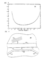
- FIG. 3 shows a graph 200 representing the relationship of surface acoustic wave frequency to the interaction length L of the multimode section 105 of FIG. 2 for achieving a complete transfer of light signal power from the even transmission mode to the next higher, odd transmission mode.
- the modulator characterized by the graph 200 employs a multimode waveguide section 105 having an approximate width and height of 5 ⁇ m and 2 ⁇ m, respectively, and a refractive index of about 1.5 relative to a refractive index of approximately 1.46 for the surrounding silica glass cladding 20, shown in FIG. 1.
- the modulator waveguide structure characterized by the graph 200 employs a SAW source 5 providing an acoustical power of approximately 1.0 W per centimeter over the length L of the multimode waveguide section 105.
- the graph 200 illustrates that it is possible to employ an interaction length L on the order of 2.0 cm to 5.0 cm to achieve a full exchange of light signal power between transmission modes with a surface acoustic wave frequency in the range of approximately 100 to 900
- the optional damper 30 absorbs and/or dampens acoustic wave energy to provide an impediment to reflection of such acoustic energy back at the waveguide structure 15. It is possible that such acoustic wave reflections would propagate through the multimode section 105 at angles other than the desired phase matching angle ⁇ causing a degradation in the coupling performance. Such reflections can occur at the edges and other surfaces of the silica optical structure 10, or other components formed within the silica glass 20.
- the particular configuration used for the damper 30 is not critical to practicing the invention. Accordingly, the damper 30 including the trench 35 containing the acoustic energy absorbing material 40 is for illustration purposes only.
- An exemplary acoustic energy absorbing material is, for example, conventional epoxy.
- a damper 30 it is advantageous to position such a damper 30 such that the waveguide structure 15 is located between the SAW source 5 and the damper 30 to allow generated surface acoustic waves to propagate into and thorough the waveguide structure 15.
- a damper according to the invention it is possible for a damper according to the invention to be an acoustic energy absorbing material, such as epoxy, formed on edge surfaces of the silica optical structure 10 as well as on the surface 11 to prevent acoustic wave reflections at such surfaces.
- Other exemplary damper configurations useable according to the invention include other adhesives such as silicone. It is also possible to provide an acousto-optic modulator according to the invention without the damper 30 of FIG. 1.
- the exemplary optical component configuration of FIGS. 1 and 2 employs the coupling of transmission modes in a multimode planar waveguide connected between input and output waveguide sections for advantageously modulating an optical signal according to the invention.
- modulator arrangement is depicted for illustration purposes only and not meant to a limitation of the invention.
- waveguide structures having single mode waveguides positioned relative to such multimode waveguides to achieve evanescent field couplings between the waveguides for modulating optical signals propagating in the single mode waveguide.
- Power of an optical signal launched in a planar or optical fiber waveguide propagates in the waveguide core as well as in evanescent field regions within the silica glass surrounding the waveguide core.
- An evanescent field coupling is achieved between particular transmission modes of two waveguides by positioning the waveguides at a particular separation distance from one another such that their evanescent field regions overlaps the core of the other waveguide.
- Evanescent field coupling enables power of an optical signal propagating in the first waveguide to be substantially transferred to a second waveguide if the coupling distance between the waveguides is maintained for a particular field interaction length.
- FIG. 4 depicts a top view of an exemplary modulator configuration 300 having a single mode planar waveguide 305 having its transmission mode coupled by evanescent field coupling to an even transmission mode of a multimode waveguide.
- FIG. 4 shows a top view of the waveguide structure 300.
- the planar single mode waveguide 305 is formed at a distance D from the multimode planar waveguide 310 along a field interaction length L E of the respective waveguides 305 and 310.
- the multimode waveguide 310 has a cross-sectional shape for propagating an optical signal in a first, even transmission mode as well as a second, next higher order, odd transmission mode.
- surface acoustic wave generated by a SAW source such as the SAW source 5 of FIG.
- Phase fronts of the surface acoustic wave are represented by reference number 125 as in FIG. 2.
- the SAW source producing the acoustic wave phase fronts 125 has not been shown in FIG. 4 for ease of illustration.
- the waveguides 305 and 310 are at a separation distance D from one another over the interaction length L E to achieve an overlap of evanescent fields of optical signals propagating in the transmission mode of the single mode waveguide 305 and the even transmission mode of the multimode waveguide 310.
- the field interaction length L E and separation distance D are selected such that power of an optical signal propagating in the single mode waveguide 305 is substantially transferred to the even transmission mode of the multimode waveguide 310 and back again to the transmission mode of the waveguide 305.
- the field interaction length L E is at least an order of magnitude larger than the value A to achieve the desired evanescent field coupling.
- a generally desirable separation distance D is typically no greater than approximately one wavelength of light of an optical signal propagating in the waveguide 310 for employing an advantageously short field interaction length L E on the order of millimeters to several centimeters for modulating an optical signal having a wavelength in the range of 1.25 ⁇ m to 1.6 ⁇ m. Greater separation distances D are useable with corresponding longer field interaction lengths L E according to the invention.
- power of an optical signal launched in an input 315 of the single mode waveguide 305 is transferred by the evanescent field coupling to the even transmission mode of the multimode waveguide 305 and back to the single mode waveguide 305 over the field interaction length L E to propagate through output section 320 of the waveguide 305.
- surface acoustic wave 125 when surface acoustic wave 125 is generated, it interacts with the multimode waveguide 310 causing a particular periodic refractive index change in the multimode waveguide 305 as is previously described with respect to FIG. 2.
- This periodic refractive index change causes power of the transferred optical signal propagating in the even transmission mode of the multimode waveguide 310 to further transfer to the next higher order, odd transmission mode of that waveguide.
- the optical signal power propagating in the even transmission mode of the waveguide 310 is attenuated, accordingly.
- Such attenuation occurs prior to the transference of optical signal power back to the single mode waveguide 305 over the interaction length L E .
- the optical signal propagating through the output section 320 of the single mode waveguide 305 is correspondingly attenuated.
- the optical signal power transferred to the odd transmission mode of the waveguide 310 due to the acousto-optic coupling is dissipated as radiation in a substantially similar manner to that previously described with regard to the multimode section 105 of FIG. 2.
- the extent of the coupling of the even and odd transmission modes of the waveguide 310 is based on the power of the surface acoustic wave interacting with the waveguide 310. Accordingly, it is possible to modulate an optical signal propagating in the waveguide 305 with a second signal by varying the power of the surface acoustic wave interacting with the waveguide 310 in accordance with the amplitude variation of this second signal.
- FIG. 5 shows an exemplary modulator configuration 400 according to the invention that is similar to the configuration 300 of FIG. 4 but that employs a single mode optical fiber waveguide 405 instead of the single mode planar waveguide of the configuration 300.
- the multimode planar waveguides 310 in the configurations 300 and 400 perform substantially identical functions and are like numbered for clarity of explanation. However, in FIG. 5, the multimode planar waveguide 310 is shown as dashed lines formed within silica glass structure 415.
- the optical fiber 405 has a core 420 positioned over the multimode planar waveguide 310. Cladding 425 surrounding the optical fiber core 420 is removed in a region proximate the multimode planar waveguide 310 enabling the desired evanescent field coupling along field interaction length L E of the waveguides 405 and 310.
- the depicted field interaction length L E extending for the entire length of the silica glass structure is for illustration purposes only and is not meant to be a limitation of the invention. It is alternatively possible to use a field interaction length L E that extends less than the entire length of the silica glass structure.
- a gap is provided between the optical fiber waveguide 310 and the multimode waveguide 405 to protect surface acoustic wave power from being dissipated by physical contact between the optical fiber 310 and the silica glass structure 415. It is desirable to use a separation distance D between the optical fiber 310 and the silica glass structure 415 in forming the gap of ) 0.5 ⁇ m or less, and preferably 0.1 ⁇ m or less to maintain an advantageously short interaction length. It is possible for such a gap to be, for example, an air gap or filled with a low density material enabling the exchange power between the waveguides 405 and 310.
- a SAW source 430 is positioned on a top surface 435 of the silica glass structure 415 for generating a surface acoustic wave at the needed relative phase matching angle ⁇ to the planar waveguide 310.
- a SAW source 430 is positioned on a top surface 435 of the silica glass structure 415 for generating a surface acoustic wave at the needed relative phase matching angle ⁇ to the planar waveguide 310.
- the modulator configurations 300 and 400 of FIGS. 4 and 5 have been described as having field interaction lengths L E and waveguide separation distances D that enabled a substantially complete transfer of power back to the single mode waveguides 305 and 405 from the planar multimode waveguide 310 due to the evanescent coupling.
- Such field interaction lengths L E and waveguide separation distances D are for illustration purposes only and not meant to be a limitation of the invention. It is alternatively possible to employ interaction lengths L E and waveguide separation distances D that enable only a partial transfer of power back to the single mode waveguides 305 and 405 from the planar multimode waveguide 310 due to the evanescent coupling.
- the resulting optical signals propagating in the single mode waveguides 305 and 405 would be scaled, accordingly, relative to the original launched optical signals.
- modulators configurations in FIGS. 1, 2, 4 and 5 are formed within a single silica optical circuit structures, it is also desirable to form such modulators within an integrated optical circuit containing other devices to produce a desired integrated optical signal processing structure having compact dimensions.
Landscapes
- Physics & Mathematics (AREA)
- Nonlinear Science (AREA)
- General Physics & Mathematics (AREA)
- Optics & Photonics (AREA)
- Optical Integrated Circuits (AREA)
- Optical Modulation, Optical Deflection, Nonlinear Optics, Optical Demodulation, Optical Logic Elements (AREA)
Applications Claiming Priority (2)
| Application Number | Priority Date | Filing Date | Title |
|---|---|---|---|
| US861287 | 1997-05-21 | ||
| US08/861,287 US5841913A (en) | 1997-05-21 | 1997-05-21 | Acousto-optic planar waveguide modulators |
Publications (2)
| Publication Number | Publication Date |
|---|---|
| EP0880048A1 true EP0880048A1 (fr) | 1998-11-25 |
| EP0880048B1 EP0880048B1 (fr) | 2001-06-06 |
Family
ID=25335396
Family Applications (1)
| Application Number | Title | Priority Date | Filing Date |
|---|---|---|---|
| EP98303702A Expired - Lifetime EP0880048B1 (fr) | 1997-05-21 | 1998-05-12 | Modulateurs acousto-optiques comprenant des guides d'ondes planaires |
Country Status (4)
| Country | Link |
|---|---|
| US (1) | US5841913A (fr) |
| EP (1) | EP0880048B1 (fr) |
| JP (1) | JP3261097B2 (fr) |
| DE (1) | DE69800880T2 (fr) |
Families Citing this family (9)
| Publication number | Priority date | Publication date | Assignee | Title |
|---|---|---|---|---|
| KR100350413B1 (ko) * | 2000-10-02 | 2002-08-28 | (주)젠포토닉스 | 외부 조절이 가능한 광도파로형 고차모드 발생기 |
| WO2002049984A1 (fr) | 2000-12-20 | 2002-06-27 | Murata Manufacturing Co.,Ltd. | Ceramique transparente, procede de production de celle-ci et element optique |
| US6868222B2 (en) * | 2002-07-01 | 2005-03-15 | Agilent Technologies, Inc. | Optical attenuator using a perturbation element with a multi-mode waveguide |
| US8578759B2 (en) * | 2010-11-15 | 2013-11-12 | The United States Of America, As Represented By The Secretary Of The Navy | Undersea pipeline intrusion detection system using low-frequency guided acoustic waves and distributed optical fiber |
| US10429677B2 (en) | 2016-09-20 | 2019-10-01 | Honeywell International Inc. | Optical waveguide having a wide brillouin bandwidth |
| US10254481B2 (en) | 2016-09-20 | 2019-04-09 | Honeywell International Inc. | Integrated waveguide with reduced brillouin gain and a corresponding reduction in the magnitude of an induced stokes wave |
| US10281646B2 (en) | 2016-09-20 | 2019-05-07 | Honeywell International Inc. | Etchless acoustic waveguiding in integrated acousto-optic waveguides |
| US10312658B2 (en) | 2017-06-22 | 2019-06-04 | Honeywell International Inc. | Brillouin gain spectral position control of claddings for tuning acousto-optic waveguides |
| US11454837B2 (en) * | 2019-11-22 | 2022-09-27 | Eagle Technology, Llc | AOM system with interface board and signal vias and related methods |
Citations (3)
| Publication number | Priority date | Publication date | Assignee | Title |
|---|---|---|---|---|
| JPH05196979A (ja) * | 1992-01-20 | 1993-08-06 | Nippon Telegr & Teleph Corp <Ntt> | 光導波路型光周波数変換器 |
| WO1994006053A1 (fr) * | 1992-09-10 | 1994-03-17 | Robert Bosch Gmbh | Composant acousto-optique integre |
| WO1995022783A1 (fr) * | 1994-02-18 | 1995-08-24 | University Of Southampton | Dispositif optique |
Family Cites Families (4)
| Publication number | Priority date | Publication date | Assignee | Title |
|---|---|---|---|---|
| US4991923A (en) * | 1989-01-17 | 1991-02-12 | Board Of Trustees Of The Leland Stanford Junior University | Acousto-optic modulator for optical fibers using Hertzian contact with a grooved transducer substrate |
| US5164628A (en) * | 1990-05-21 | 1992-11-17 | Canon Kabushiki Kaisha | Elastic surface wave convolva having wave width converting means and communication system using same |
| US5367216A (en) * | 1991-08-02 | 1994-11-22 | Canon Kabushiki Kaisha | Surface acoustic wave element and communication system using the same |
| JP2920738B2 (ja) * | 1995-06-15 | 1999-07-19 | 株式会社村田製作所 | 音響光学偏向素子 |
-
1997
- 1997-05-21 US US08/861,287 patent/US5841913A/en not_active Expired - Lifetime
-
1998
- 1998-05-12 EP EP98303702A patent/EP0880048B1/fr not_active Expired - Lifetime
- 1998-05-12 DE DE69800880T patent/DE69800880T2/de not_active Expired - Lifetime
- 1998-05-18 JP JP13570498A patent/JP3261097B2/ja not_active Expired - Fee Related
Patent Citations (3)
| Publication number | Priority date | Publication date | Assignee | Title |
|---|---|---|---|---|
| JPH05196979A (ja) * | 1992-01-20 | 1993-08-06 | Nippon Telegr & Teleph Corp <Ntt> | 光導波路型光周波数変換器 |
| WO1994006053A1 (fr) * | 1992-09-10 | 1994-03-17 | Robert Bosch Gmbh | Composant acousto-optique integre |
| WO1995022783A1 (fr) * | 1994-02-18 | 1995-08-24 | University Of Southampton | Dispositif optique |
Non-Patent Citations (2)
| Title |
|---|
| GOTO NOBUO ET AL: "OPTICAL SIGNAL PROCESSORS CONSISTING OF COLLINEAR ACOUSTO-OPTIC CHANNEL WAVEGUIDES", ICASSP 86 - PROCEEDINGS, IEEE-IECEJ-ASJ INTERNATIONAL CONFERENCE ON ACOUSTICS, SPEECH, AND SIGNAL PROCESSING.;TOKYO, JPN, 1986, PROC ICASSP IEEE INT CONF ACOUST SPEECH SIGNAL PROCESS 1986 IEEE, NEW YORK, NY, USA, pages 489 - 492, XP002073942 * |
| PATENT ABSTRACTS OF JAPAN vol. 017, no. 621 (P - 1645) 16 November 1993 (1993-11-16) * |
Also Published As
| Publication number | Publication date |
|---|---|
| DE69800880D1 (de) | 2001-07-12 |
| JP3261097B2 (ja) | 2002-02-25 |
| EP0880048B1 (fr) | 2001-06-06 |
| US5841913A (en) | 1998-11-24 |
| JPH10319363A (ja) | 1998-12-04 |
| DE69800880T2 (de) | 2002-03-28 |
Similar Documents
| Publication | Publication Date | Title |
|---|---|---|
| US6243516B1 (en) | Merging optical waveguides having branch angle within a specific range | |
| US7058261B2 (en) | Interfacing multiple wavelength sources to thin optical waveguides utilizing evanescent coupling | |
| US6571039B1 (en) | Optical waveguide having a weakly-confining waveguide section and a strongly-confining waveguide section optically coupled by a tapered neck | |
| EP0877284B1 (fr) | Commutateur acousto-optique pour circuit optique en silice | |
| US4881791A (en) | Optical device | |
| EP3874308B1 (fr) | Procédé et appareil de commande et de suppression de lumière parasite dans un circuit intégré photonique | |
| US5708736A (en) | Optical waveguide mode coupling using mechanical wave interference | |
| JP2005538426A (ja) | 埋め込みモードコンバータ | |
| US5471545A (en) | Optical external modulator for optical telecommunications | |
| US6804440B2 (en) | Integrated mode converter, waveguide, and on-chip function | |
| TW200305740A (en) | High density integrated optical chip | |
| EP0880048B1 (fr) | Modulateurs acousto-optiques comprenant des guides d'ondes planaires | |
| JP3456166B2 (ja) | フォトニック結晶を用いた光結合素子および光結合方法 | |
| CN107884961A (zh) | 一种基于声光作用的全光纤反射式光学移频器及移频方法 | |
| WO1989001171A1 (fr) | Composants a fibre optique | |
| US6868210B2 (en) | Optical waveguide and their application of the optical communication system | |
| US20040264827A1 (en) | Optical modulator | |
| Mao et al. | An ARROW optical wavelength filter: design and analysis | |
| EP0859264B1 (fr) | Modulateur acousto-optique comprenant un guide d'onde optique | |
| EP1544648B1 (fr) | Convertisseur de modes utilisant des réflecteurs omnidirectionnels | |
| JP2002169052A (ja) | 異方導光性部材を有する光学装置 | |
| JP2991261B2 (ja) | 光導波路型光周波数変換器 | |
| WO2024214248A1 (fr) | Émetteur optique, émetteur-récepteur optique l'utilisant, et système de communication optique | |
| NL8602425A (nl) | Reflector voor optische vezels. | |
| JPH04180034A (ja) | 導波路型光デバイス |
Legal Events
| Date | Code | Title | Description |
|---|---|---|---|
| PUAI | Public reference made under article 153(3) epc to a published international application that has entered the european phase |
Free format text: ORIGINAL CODE: 0009012 |
|
| 17P | Request for examination filed |
Effective date: 19980521 |
|
| AK | Designated contracting states |
Kind code of ref document: A1 Designated state(s): DE FR GB NL |
|
| AX | Request for extension of the european patent |
Free format text: AL;LT;LV;MK;RO;SI |
|
| 17Q | First examination report despatched |
Effective date: 19990423 |
|
| AKX | Designation fees paid |
Free format text: DE FR GB NL |
|
| GRAG | Despatch of communication of intention to grant |
Free format text: ORIGINAL CODE: EPIDOS AGRA |
|
| GRAG | Despatch of communication of intention to grant |
Free format text: ORIGINAL CODE: EPIDOS AGRA |
|
| GRAH | Despatch of communication of intention to grant a patent |
Free format text: ORIGINAL CODE: EPIDOS IGRA |
|
| GRAH | Despatch of communication of intention to grant a patent |
Free format text: ORIGINAL CODE: EPIDOS IGRA |
|
| GRAA | (expected) grant |
Free format text: ORIGINAL CODE: 0009210 |
|
| AK | Designated contracting states |
Kind code of ref document: B1 Designated state(s): DE FR GB NL |
|
| PG25 | Lapsed in a contracting state [announced via postgrant information from national office to epo] |
Ref country code: NL Free format text: LAPSE BECAUSE OF FAILURE TO SUBMIT A TRANSLATION OF THE DESCRIPTION OR TO PAY THE FEE WITHIN THE PRESCRIBED TIME-LIMIT Effective date: 20010606 |
|
| REF | Corresponds to: |
Ref document number: 69800880 Country of ref document: DE Date of ref document: 20010712 |
|
| NLV1 | Nl: lapsed or annulled due to failure to fulfill the requirements of art. 29p and 29m of the patents act | ||
| ET | Fr: translation filed | ||
| REG | Reference to a national code |
Ref country code: GB Ref legal event code: IF02 |
|
| PLBE | No opposition filed within time limit |
Free format text: ORIGINAL CODE: 0009261 |
|
| STAA | Information on the status of an ep patent application or granted ep patent |
Free format text: STATUS: NO OPPOSITION FILED WITHIN TIME LIMIT |
|
| 26N | No opposition filed | ||
| PGFP | Annual fee paid to national office [announced via postgrant information from national office to epo] |
Ref country code: GB Payment date: 20140507 Year of fee payment: 17 |
|
| PGFP | Annual fee paid to national office [announced via postgrant information from national office to epo] |
Ref country code: FR Payment date: 20140509 Year of fee payment: 17 Ref country code: DE Payment date: 20140507 Year of fee payment: 17 |
|
| REG | Reference to a national code |
Ref country code: DE Ref legal event code: R082 Ref document number: 69800880 Country of ref document: DE Representative=s name: DILG HAEUSLER SCHINDELMANN PATENTANWALTSGESELL, DE |
|
| REG | Reference to a national code |
Ref country code: DE Ref legal event code: R119 Ref document number: 69800880 Country of ref document: DE |
|
| GBPC | Gb: european patent ceased through non-payment of renewal fee |
Effective date: 20150512 |
|
| REG | Reference to a national code |
Ref country code: FR Ref legal event code: ST Effective date: 20160129 |
|
| PG25 | Lapsed in a contracting state [announced via postgrant information from national office to epo] |
Ref country code: DE Free format text: LAPSE BECAUSE OF NON-PAYMENT OF DUE FEES Effective date: 20151201 Ref country code: GB Free format text: LAPSE BECAUSE OF NON-PAYMENT OF DUE FEES Effective date: 20150512 |
|
| PG25 | Lapsed in a contracting state [announced via postgrant information from national office to epo] |
Ref country code: FR Free format text: LAPSE BECAUSE OF NON-PAYMENT OF DUE FEES Effective date: 20150601 |