EP0880179A2 - Configuration d'ouvertures d'échappement pour structures conducteur-dielectrique multicouches - Google Patents
Configuration d'ouvertures d'échappement pour structures conducteur-dielectrique multicouches Download PDFInfo
- Publication number
- EP0880179A2 EP0880179A2 EP98304020A EP98304020A EP0880179A2 EP 0880179 A2 EP0880179 A2 EP 0880179A2 EP 98304020 A EP98304020 A EP 98304020A EP 98304020 A EP98304020 A EP 98304020A EP 0880179 A2 EP0880179 A2 EP 0880179A2
- Authority
- EP
- European Patent Office
- Prior art keywords
- conductive layer
- conductive
- layer
- aperture
- area
- Prior art date
- Legal status (The legal status is an assumption and is not a legal conclusion. Google has not performed a legal analysis and makes no representation as to the accuracy of the status listed.)
- Withdrawn
Links
Images


Classifications
-
- H—ELECTRICITY
- H05—ELECTRIC TECHNIQUES NOT OTHERWISE PROVIDED FOR
- H05K—PRINTED CIRCUITS; CASINGS OR CONSTRUCTIONAL DETAILS OF ELECTRIC APPARATUS; MANUFACTURE OF ASSEMBLAGES OF ELECTRICAL COMPONENTS
- H05K1/00—Printed circuits
- H05K1/02—Details
- H05K1/0213—Electrical arrangements not otherwise provided for
- H05K1/0216—Reduction of cross-talk, noise or electromagnetic interference
- H05K1/0218—Reduction of cross-talk, noise or electromagnetic interference by printed shielding conductors, ground planes or power plane
- H05K1/0224—Patterned shielding planes, ground planes or power planes
-
- H—ELECTRICITY
- H10—SEMICONDUCTOR DEVICES; ELECTRIC SOLID-STATE DEVICES NOT OTHERWISE PROVIDED FOR
- H10W—GENERIC PACKAGES, INTERCONNECTIONS, CONNECTORS OR OTHER CONSTRUCTIONAL DETAILS OF DEVICES COVERED BY CLASS H10
- H10W70/00—Package substrates; Interposers; Redistribution layers [RDL]
- H10W70/60—Insulating or insulated package substrates; Interposers; Redistribution layers
- H10W70/611—Insulating or insulated package substrates; Interposers; Redistribution layers for connecting multiple chips together
-
- H—ELECTRICITY
- H10—SEMICONDUCTOR DEVICES; ELECTRIC SOLID-STATE DEVICES NOT OTHERWISE PROVIDED FOR
- H10W—GENERIC PACKAGES, INTERCONNECTIONS, CONNECTORS OR OTHER CONSTRUCTIONAL DETAILS OF DEVICES COVERED BY CLASS H10
- H10W70/00—Package substrates; Interposers; Redistribution layers [RDL]
- H10W70/60—Insulating or insulated package substrates; Interposers; Redistribution layers
- H10W70/62—Insulating or insulated package substrates; Interposers; Redistribution layers characterised by their interconnections
- H10W70/65—Shapes or dispositions of interconnections
-
- H—ELECTRICITY
- H10—SEMICONDUCTOR DEVICES; ELECTRIC SOLID-STATE DEVICES NOT OTHERWISE PROVIDED FOR
- H10W—GENERIC PACKAGES, INTERCONNECTIONS, CONNECTORS OR OTHER CONSTRUCTIONAL DETAILS OF DEVICES COVERED BY CLASS H10
- H10W70/00—Package substrates; Interposers; Redistribution layers [RDL]
- H10W70/60—Insulating or insulated package substrates; Interposers; Redistribution layers
- H10W70/67—Insulating or insulated package substrates; Interposers; Redistribution layers characterised by their insulating layers or insulating parts
- H10W70/68—Shapes or dispositions thereof
- H10W70/685—Shapes or dispositions thereof comprising multiple insulating layers
-
- H—ELECTRICITY
- H05—ELECTRIC TECHNIQUES NOT OTHERWISE PROVIDED FOR
- H05K—PRINTED CIRCUITS; CASINGS OR CONSTRUCTIONAL DETAILS OF ELECTRIC APPARATUS; MANUFACTURE OF ASSEMBLAGES OF ELECTRICAL COMPONENTS
- H05K1/00—Printed circuits
- H05K1/02—Details
- H05K1/0213—Electrical arrangements not otherwise provided for
- H05K1/0237—High frequency adaptations
- H05K1/025—Impedance arrangements, e.g. impedance matching, reduction of parasitic impedance
- H05K1/0253—Impedance adaptations of transmission lines by special lay-out of power planes, e.g. providing openings
-
- H—ELECTRICITY
- H05—ELECTRIC TECHNIQUES NOT OTHERWISE PROVIDED FOR
- H05K—PRINTED CIRCUITS; CASINGS OR CONSTRUCTIONAL DETAILS OF ELECTRIC APPARATUS; MANUFACTURE OF ASSEMBLAGES OF ELECTRICAL COMPONENTS
- H05K2201/00—Indexing scheme relating to printed circuits covered by H05K1/00
- H05K2201/06—Thermal details
- H05K2201/062—Means for thermal insulation, e.g. for protection of parts
-
- H—ELECTRICITY
- H05—ELECTRIC TECHNIQUES NOT OTHERWISE PROVIDED FOR
- H05K—PRINTED CIRCUITS; CASINGS OR CONSTRUCTIONAL DETAILS OF ELECTRIC APPARATUS; MANUFACTURE OF ASSEMBLAGES OF ELECTRICAL COMPONENTS
- H05K2201/00—Indexing scheme relating to printed circuits covered by H05K1/00
- H05K2201/09—Shape and layout
- H05K2201/09209—Shape and layout details of conductors
- H05K2201/09654—Shape and layout details of conductors covering at least two types of conductors provided for in H05K2201/09218 - H05K2201/095
- H05K2201/09681—Mesh conductors, e.g. as a ground plane
-
- H—ELECTRICITY
- H05—ELECTRIC TECHNIQUES NOT OTHERWISE PROVIDED FOR
- H05K—PRINTED CIRCUITS; CASINGS OR CONSTRUCTIONAL DETAILS OF ELECTRIC APPARATUS; MANUFACTURE OF ASSEMBLAGES OF ELECTRICAL COMPONENTS
- H05K2203/00—Indexing scheme relating to apparatus or processes for manufacturing printed circuits covered by H05K3/00
- H05K2203/11—Treatments characterised by their effect, e.g. heating, cooling, roughening
- H05K2203/1178—Means for venting or for letting gases escape
-
- H—ELECTRICITY
- H05—ELECTRIC TECHNIQUES NOT OTHERWISE PROVIDED FOR
- H05K—PRINTED CIRCUITS; CASINGS OR CONSTRUCTIONAL DETAILS OF ELECTRIC APPARATUS; MANUFACTURE OF ASSEMBLAGES OF ELECTRICAL COMPONENTS
- H05K3/00—Apparatus or processes for manufacturing printed circuits
- H05K3/46—Manufacturing multilayer circuits
- H05K3/4644—Manufacturing multilayer circuits by building the multilayer layer by layer, i.e. build-up multilayer circuits
-
- Y—GENERAL TAGGING OF NEW TECHNOLOGICAL DEVELOPMENTS; GENERAL TAGGING OF CROSS-SECTIONAL TECHNOLOGIES SPANNING OVER SEVERAL SECTIONS OF THE IPC; TECHNICAL SUBJECTS COVERED BY FORMER USPC CROSS-REFERENCE ART COLLECTIONS [XRACs] AND DIGESTS
- Y10—TECHNICAL SUBJECTS COVERED BY FORMER USPC
- Y10T—TECHNICAL SUBJECTS COVERED BY FORMER US CLASSIFICATION
- Y10T428/00—Stock material or miscellaneous articles
- Y10T428/24—Structurally defined web or sheet [e.g., overall dimension, etc.]
- Y10T428/24273—Structurally defined web or sheet [e.g., overall dimension, etc.] including aperture
- Y10T428/24298—Noncircular aperture [e.g., slit, diamond, rectangular, etc.]
- Y10T428/24314—Slit or elongated
-
- Y—GENERAL TAGGING OF NEW TECHNOLOGICAL DEVELOPMENTS; GENERAL TAGGING OF CROSS-SECTIONAL TECHNOLOGIES SPANNING OVER SEVERAL SECTIONS OF THE IPC; TECHNICAL SUBJECTS COVERED BY FORMER USPC CROSS-REFERENCE ART COLLECTIONS [XRACs] AND DIGESTS
- Y10—TECHNICAL SUBJECTS COVERED BY FORMER USPC
- Y10T—TECHNICAL SUBJECTS COVERED BY FORMER US CLASSIFICATION
- Y10T428/00—Stock material or miscellaneous articles
- Y10T428/24—Structurally defined web or sheet [e.g., overall dimension, etc.]
- Y10T428/24273—Structurally defined web or sheet [e.g., overall dimension, etc.] including aperture
- Y10T428/24322—Composite web or sheet
- Y10T428/24331—Composite web or sheet including nonapertured component
Definitions
- the present invention relates to the construction of multilayer conductor-dielectric structures that may be found in Multichip Modules (MCMs) and the like, and more specifically to preventing delamination of layers in such structures.
- MCMs Multichip Modules
- interconnect structures found in the electronic industry comprise alternating layers of dielectric material and metal.
- One common interconnect structure comprises alternating layers of a polymeric material, such as polyimide, and copper.
- a polymeric material such as polyimide
- Such structures usually begin with a base substrate, such as a silicon wafer, which is coated with a layer of polyimide using a spin-on coating process, much like that used to apply a photoresist layer. Thereafter, the starting polyimide layer is soft baked, and then cured. The curing step imidizes ( i.e., cross-links) the polymer chains of the polyimide material.
- the polyimide may be cured by exposure to heat, ultraviolet light, electron beam radiation, or a combination thereof.
- a metal layer is then formed over the starting polyimide layer and patterned to provide the desired electrical interconnects for that layer.
- the metal layer may be formed by sputter coating a seed layer of material, such as chromium, followed by an electroplating process.
- the resulting metal layer may then be patterned by selectively etching the material through a patterned photoresist layer, as is well known in the semiconductor processing art.
- a second polyimide layer is then formed over the first metal layer, and then soft baked. However, before curing the second polyimide layer, the layer is usually patterned to form vias, or apertures, through the second polyimide layer to parts of the underlying first metal layer.
- vias will enable vertical electrical connections to be made between signal lines in the first metal layer, and signal lines in a second metal layer which will be subsequently formed over the second polyimide layer.
- the vias may be made by the conventional photoresist/etching steps, or a photo-imageable polyimide may be used.
- the vias are then filled with metal, which may be done by an electroless plating or electroplating process.
- a second metal layer is formed and patterned, which may be done with the same steps used to form and pattern the first layer.
- the number of polyimide and metal layers constructed depends upon the design and purpose of the structure.
- the multilayer ceramic art which is a more mature technology, has a similar structure of alternating dielectric and metal layers.
- the dielectric layers are raw, un-fired sheets of ceramic material (so-called "green-sheets"), upon which the metal layers are formed by screening metallic paste over the raw sheets through patterns. After screening, the raw sheets are pressed together and heated to a high temperature to cure the raw sheets. The heating process is known as a "firing" step.
- the multilayer ceramic structures use AC ground planes on either side of one or more of the metal signal layers, with a dielectric ceramic layer separating each AC grounding plane from each metal signal layer.
- AC grounding planes are used to provide each signal line with a controlled impedance characteristic, and to reduce the coupling of electromagnetic energy between adjacent signal lines (so called "cross-talk") by establishing a desired electromagnetic field pattern between each signal line and the AC grounding layers.
- the controlled impedance characteristic also enables the designer to better estimate the signal propagation characteristics of the signal lines. The design of such structures is well know in the microstrip and slot-line arts, which are part of the electromagnetic wave propagation art.
- the above delamination process may also occur when an upper polyimide layer is being cured by a heat treatment, or by other heat treatments which may be needed in the manufacturing of the multilayer substrate.
- polyimide layers which may not have been fully cured may release gases that are generated as part of the imidization process.
- various photo-active compounds in photo-imageable polyimides may undergo decompositions which create additional gases.
- Most other types of polymeric materials suffer the above same problems, so that switching to a different type of dielectric material does not solve the above problems.
- An embodiment of the present invention makes use of the appreciation that the build up of gases within polymeric layers, such as polyimide, can be prevented by providing venting apertures, or holes, within the AC grounding planes (and the like).
- the diameter needed by such holes to vent the gases is relatively large, which causes at least two problems.
- the large diameter reduces the planarity of the dielectric layer which overlies the grounding plane.
- the apertures can create disturbances in the electromagnetic field lines between the metal signal lines and the AC grounding planes, and thereby ruin the ability of the grounding plane to provide a controlled impedance characteristic and to prevent signal "cross-talk.”
- the latter problem is most ncticeable for signals which are transmitted at frequencies of 200 MHz and above.
- Embodiments of the present invention can alter the design of AC grounding planes, and similar structures such as power distribution planes, so as to prevent the problems and dissatis mentioned above.
- FIG. 1 is a top plan view of a first embodiment of a venting structure according to the present invention.
- FIG. 2 is a partial cross-sectional view of the embodiment shown in FIG. 1 according to the present invention taken along the line 2-2 shown in FIG. 1.
- FIG. 3 is a top plan view of an array of venting structures shown in FIGS. 1 and 2 according to the present invention.
- FIG. 4 is a top plan view of a second embodiment of a venting structure according to the present invention.
- FIG. 5 is a top plan view of a third embodiment of a venting structure according to the present invention.
- FIG. 6 is a top plan view of a fourth embodiment of a venting structure according to the present invention.
- FIG. 7 is a partial cross-sectional view of the embodiment shown in FIG. 6 according to the present invention taken along the line 7-7 shown in FIG. 6.
- FIG. 8 is a top plan view showing a radial arrangement of venting structures shown in FIGS. 6 and 7.
- FIG. 9 is a top plan view of additional embodiments of venting structures according to the present invention.
- FIG. 10 is a top plan view of a yet another embodiment of a venting structure according to the present invention.
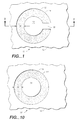
- FIG. 1 shows a top plan view of a first embodiment of a venting structure 10 according to the present invention
- FIG. 2 shows a cross-sectional view thereof along the line 2-2 shown in FIG. 1.
- the venting structure 10 is formed within a metal layer 12, which may serve as an AC grounding plane or power distribution plane, or the like.
- Metal layer 12 is disposed upon a dielectric layer 11, which is in turn disposed upon a silicon substrate 5, or the like.
- dielectric layer 11 comprises a polymeric material, such as polyimide
- metal layer 12 comprises a highly conductive material, such as copper.
- a second dielectric layer 13, preferably comprising a polymeric material or polyimide, is disposed upon metal layer 12.
- Venting structure 10 comprises an aperture 14 formed in metal layer 12.
- Aperture 14 may have any shape, and has a perimeter which encompasses its shape.
- a conductive pad 16 which may be electrically coupled to metal layer 12 by a conductive bridge, or path, 18.
- Pad 16, bridge 18, and metal layer 12 may all be formed in the same processing step and may comprise the same material. In a preferred construction, these components are formed by forming a blanket layer of metal over the entire exposed portion of dielectric layer 11, and thereafter patterning the blanket layer to define aperture 14, pad 16 and bridge 18 within layer 12.
- Conductive pad 16 preferably comprises at least approximately 30 percent of the area of aperture 14. In some implementations of venting structure 10, pad 16 may comprise approximately 50 percent or more of the area within aperture 14, and approximately 80 percent or more, particularly for venting holes with diameters which are larger than about 100 ⁇ m.
- An annular shaped gap 15 is formed between aperture 14 and the combination of pad 16 and bridge 18. Gap 15 enables gases within the underlying dielectric layer 11 to escape up towards and into the overlying second dielectric layer 13, thereby relieving pressure along the interface between dielectric layer 11 and metal layer 12.
- Conductive bridge 18 functions to electrically connect pad 16 with outer conductive layer 12 so that pad 16 may cooperate with layer 12 in terms of providing an AC grounding plane.
- the bridges 18 are primarily used in embodiments of the present invention where the signal lines carry high frequency signals (usually above about 200 MHz), where the electrical properties of the grounding plane become important. Bridges 18 are often not necessary for embodiments where lower frequency signal lines are employed, particularly where the diameter ofthe aperture 14 is less than approximately 400 ⁇ m.
- FIG. 10 shows a top plane view of a venting structure embodiment 10' which does not have a conductive bridge.
- gap 15 does not have as large a surface area as aperture 14 has, gap 15 does traverse a relatively long distance over underlying layer 11, from which it can collect vapors from underlying layer 11. Gap 15 is nearly as effective at collecting gases as aperture 14 would be without pad 16, and does not impact the performance of the signal lines near as much as aperture 14 does when used without pad 16 and bridge 18.
- aperture 14 has an outer diameter of 55 microns
- gap 15 has a width W of approximately 7.5 microns
- conductive pad 16 has a diameter of 40 microns.
- the width of bridge 18 may be on the order of 5 to 10 microns, if it is desired to use a bridge.
- conductive pad 16 has an area which is 52% of the area encompassed by aperture 14, which is over 50% of the area of aperture 14.
- the width of gap 15 is limited such that the depth of the depression does not exceed about one-half of the thickness of conductive layer 12.
- the depth of the depression is primarily dependent upon four factors: (1) the thickness of conductive layer 12, (2) the thickness of dielectric layer 13, (3) the gap width W, and (4) the physical properties of the dielectric, in the fluidized state, such as molecular weight, viscosity, and surface tension.
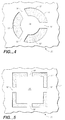
- FIG. 3 is a top plan view of an array of venting structures 10 embodying the present invention.
- the venting structures 10 are preferably distributed evenly across the surface of the substrate 5 to enable uniform venting of the gases in the underlying dielectric layer 11.
- array patterns such as a hexagonal close-pack pattern, a standard rectangular grid pattern, or a standard square grid pattern (which is shown in FIG. 3, where the pattern has been set at a 45° angle with respect to the substrate edges).
- the total area of the gaps 15 generally does not constitute more than about ten percent of the area encompassed by metal layer 12, and preferably does not constitute more than about two to five percent.
- the total gap area is less than 1 percent of the total exposed area, being in the range of 0 1 percent and 1 percent.
- the venting structures may be spaced apart from one another at a distance which is, for example, equal to two to ten times the width ( e.g. , diameter) of the structure.
- the structures are 55 ⁇ m wide, and are spaced apart from one another by distance of between 250 ⁇ m (approximately five-times) and 330 ⁇ m (six-times).
- the structures are approximately 55 ⁇ m wide, and are spaced apart from one another by distance of approximately 305 ⁇ m (5.55 times).
- layer 12 is approximately, 5 ⁇ m to 8 ⁇ m thick, the surrounding dielectric layers are from approximately 5 ⁇ m to 15 ⁇ m thick, and gap 15 is approximately 7.5 ⁇ m wide, and bridge 18 are not used.
- the dimensions of the venting structure are the same as above, but the venting structures are spaced apart from one another by distance of approximately 153 ⁇ m (one-half of 305 ⁇ m).
- layer 12 is approximately 5 ⁇ m thick, and the surrounding dielectric layers are from approximately 5 ⁇ m to 15 ⁇ m thick.
- the patterns of venting structures may be stacked over one another to provide for good venting of gases.
- polyimide materials in which the diffusivity of the water vapor (steam) is substantially the same in the vertical and lateral directions (so-called isotropic polyimide polymers), and in which the thickness of the polyimide is less than 30 ⁇ m.
- Most polyimide materials have isotropic diffusivity.
- some polyimide materials have anisotropic diffusivity where the water vapor diffuses faster in one direction than the other directions.
- the diffusivity values are larger in the lateral directions than in the vertical direction.
- the anisotropic characteristic may affect the selection of the vent hole size and pitch. For example, larger lateral diffusivities would enable the venting holes to be spaced further apart from that expected from the vertical diffusivity.
- venting structure 20 has substantially the same structure as venting structure 10 except that it includes two additional bridges 18 for a total of three such bridges.
- the bridges 18 are divided roughly equally around the circumference of aperture 14, and thereby divide up the original gap 15 into three gaps 15'.
- the additional bridges provide the advantage of increasing electrical conductivity to pad 16, which improves its ability to act as a grounding plane at high signal frequencies by enabling currents in the grounding plane to flow to pad 16 by more than just one direction.
- the additional bridges 18 take up relatively little additional area, and do not substantially affect the ability of the venting structure to collect and vent vapors. Additionally, in those constructed embodiments where bridges 18 are relatively thin and might be susceptible to failure, the additional bridges 18 serve to increase the reliability and yield of the electrical connection to pad 16.
- aperture 14 may have other shapes beside the circular shape shown in FIGS. 1-4.
- triangular, rectangular, pentagonal, hexagonal, septagonal, octagonal, etc. shapes may be employed.
- FIG. 5 shows an embodiment where the aperture (which is shown at 14') has a substantially square shape.
- pad 16' may also have a square shape, and there may be four bridges 18' between pad 16' and a metal layer 12.
- FIG. 6 shows another exemplary class of embodiments of venting structures according to the present invention.
- the figure shows a top plan view of a substrate having a metal layer 12 and an underlying dielectric layer 11.
- An array of venting apertures 44 is formed uniformly over the area of metal layer 12, each venting structure 44 comprising a slit of a length which is at least three times its width, and preferably at least five times its width.
- FIG. 7 shows a partial cross-sectional view of the structure taken along the line 7-7 shown in FIG. 6.
- the slits 44 are preferably arranged in a regular pattern and their total area is at least 0.1 percent of the area encompassed by conductive layer 12, and typically in the range from 0.1 percent to 2 percent.
- the total area of slits 44 preferably does not comprise more than five to ten percent of the area encompassed by metal layer 12.
- the length of each slit 44 is at least 10 times the width of the slit, with the length being 15 times the width in one embodiment.
- the width of each slit is 10 ⁇ m, the length is 150 ⁇ m, and the slits are spaced from one another by approximately 200 ⁇ m on each side.
- venting structures described herein may be arranged in a non-uniform manner, for example when an irregular pattern is needed to accommodate the routing ofvertical vias through metal layer 12, or the routing ofvia connections to metal layer 12.
- the spacing between adjacent venting structures should not be changed by more than about a factor of two from that of a regular array patten.
- venting structures should not be placed too far away from the peripheral edge of metal layer 12.
- the distance between any point on the periphery and the closest structure should not be greater than approximately the square root of"4A" divided by "N,” which may be stated as ⁇ 2 A/N . If the construction of the dielectric and metals layers around the periphery of the metal layer 12 enables gases to be easily vented at the periphery, then this spacing distance may be substantially increased, such as to ⁇ 4 A/N and above.
- slits 44 are arranged in a regular pattern whereby their lengths are aligned to be parallel to a common axis.
- the slits may be arranged in a radial manner. An example of one such arrangement is shown in FIG. 8. It may also be appreciated that a curvilinear shape may be given to the slits, as for example the slits 54 and 64 shown in FIG. 9.
- the slits 44 may be designed in the same manner as the gaps 15, as described above (see the above formula on maximum width). For good electrical performance for signal lines operating at 200 MHz and above, the width of slits 44 and gaps 15 may be kept below about 20 ⁇ m.
- venting structures in an embodiment of the present invention may be as high as 1,000 to 1,500 structures per square centimeter, but the total gap/slit area may not comprise more than 1 to 10 percent of the area encompassed by metal layer 12, and preferably comprises between 0.1 and 5 percent of the area encompassed by metal layer 12.
- Embodiments of the present invention typically have at least 100 venting structures per square centimeter (which is at least 1,000 structures for a substrate having an area of 10 cm 2 ), and usually have at least 500 venting structures per square centimeter (which is at least 5,000 structures for a substrate having an area of 10 cm 2 ).
- venting structures per square centimeter which is at least 1,000 structures for a substrate having an area of 10 cm 2
- 500 venting structures per square centimeter which is at least 5,000 structures for a substrate having an area of 10 cm 2
- the dimensions of each individual structure should be decreased.
- Embodiments of the present invention using approximately 1,050 venting structures per square centimeter have been constructed, and embodiments with over 4,000 venting structures per square centimeter are currently being built and evaluated.
Landscapes
- Physics & Mathematics (AREA)
- Electromagnetism (AREA)
- Engineering & Computer Science (AREA)
- Microelectronics & Electronic Packaging (AREA)
- Production Of Multi-Layered Print Wiring Board (AREA)
Applications Claiming Priority (2)
| Application Number | Priority Date | Filing Date | Title |
|---|---|---|---|
| US08/859,642 US6106923A (en) | 1997-05-20 | 1997-05-20 | Venting hole designs for multilayer conductor-dielectric structures |
| US859642 | 2010-08-19 |
Publications (2)
| Publication Number | Publication Date |
|---|---|
| EP0880179A2 true EP0880179A2 (fr) | 1998-11-25 |
| EP0880179A3 EP0880179A3 (fr) | 1999-06-02 |
Family
ID=25331400
Family Applications (1)
| Application Number | Title | Priority Date | Filing Date |
|---|---|---|---|
| EP98304020A Withdrawn EP0880179A3 (fr) | 1997-05-20 | 1998-05-20 | Configuration d'ouvertures d'échappement pour structures conducteur-dielectrique multicouches |
Country Status (3)
| Country | Link |
|---|---|
| US (1) | US6106923A (fr) |
| EP (1) | EP0880179A3 (fr) |
| JP (1) | JPH10335535A (fr) |
Cited By (1)
| Publication number | Priority date | Publication date | Assignee | Title |
|---|---|---|---|---|
| WO2009010457A3 (fr) * | 2007-07-18 | 2009-04-30 | Siemens Ag | Fentes d'extension destinées à réduire les contraintes thermomécaniques d'une connexion électrique |
Families Citing this family (10)
| Publication number | Priority date | Publication date | Assignee | Title |
|---|---|---|---|---|
| JP2001007469A (ja) | 1999-06-23 | 2001-01-12 | Sony Corp | プリント配線板およびプリント配線板の製造方法 |
| JP3516611B2 (ja) * | 1999-06-29 | 2004-04-05 | シャープ株式会社 | 半導体装置、その製造方法及び半導体装置用基板 |
| USD444631S1 (en) | 2000-05-02 | 2001-07-10 | Hunt Technology Limited | Sheet material |
| US7152313B2 (en) * | 2003-11-26 | 2006-12-26 | Intel Corporation | Package substrate for integrated circuit and method of making the substrate |
| JP4543699B2 (ja) * | 2004-02-27 | 2010-09-15 | 凸版印刷株式会社 | 回路基板の実装構造 |
| JP6374338B2 (ja) * | 2015-03-24 | 2018-08-15 | 京セラ株式会社 | 配線基板 |
| JP6841342B2 (ja) | 2017-11-16 | 2021-03-10 | 株式会社村田製作所 | 樹脂多層基板、電子部品およびその実装構造 |
| WO2020129344A1 (fr) * | 2018-12-18 | 2020-06-25 | 古河電気工業株式会社 | Câble, structure de connexion pourvue d'un câble, faisceau de câbles et corps mobile amarré |
| JP7145068B2 (ja) * | 2018-12-28 | 2022-09-30 | 新光電気工業株式会社 | 配線基板及びその製造方法 |
| CN112770550B (zh) * | 2021-01-18 | 2025-08-26 | 深圳市实锐泰科技有限公司 | 一种具有排气通道柔性电路板及其制作方法 |
Family Cites Families (22)
| Publication number | Priority date | Publication date | Assignee | Title |
|---|---|---|---|---|
| US4061263A (en) * | 1976-09-22 | 1977-12-06 | International Telephone And Telegraph Corporation | Method of bonding a dielectric substrate to a metallic carrier in a printed circuit assembly |
| US4201616A (en) * | 1978-06-23 | 1980-05-06 | International Business Machines Corporation | Dimensionally stable laminated printed circuit cores or boards and method of fabricating same |
| US4350545A (en) * | 1979-10-12 | 1982-09-21 | Armen Garabedian | Method of laminating plastic sheets |
| US4522667A (en) * | 1980-06-25 | 1985-06-11 | General Electric Company | Method for making multi-layer metal core circuit board laminate with a controlled thermal coefficient of expansion |
| GB2080729A (en) * | 1980-06-25 | 1982-02-10 | Gen Electric | A multi-layer metal core circuit board laminate with a controlled thermal coefficient of expansion and method for making same. |
| US4394953A (en) * | 1981-03-12 | 1983-07-26 | Schwarzkopf Development Corporation | Method of joining individual parts of an X-ray anode, in particular of a rotating anode |
| EP0063408B1 (fr) * | 1981-03-27 | 1984-12-27 | AMP INCORPORATED (a New Jersey corporation) | Substrat en semiconducteur pour puce |
| US4409278A (en) * | 1981-04-16 | 1983-10-11 | General Electric Company | Blister-free direct bonding of metals to ceramics and metals |
| GB2099742B (en) * | 1981-06-05 | 1985-07-31 | Philips Electronic Associated | Bonding metals to non-metals |
| US4551746A (en) * | 1982-10-05 | 1985-11-05 | Mayo Foundation | Leadless chip carrier apparatus providing an improved transmission line environment and improved heat dissipation |
| US4769269A (en) * | 1983-12-05 | 1988-09-06 | E. I. Du Pont De Nemours And Company | Article containing conductive through-holes |
| US5061547A (en) * | 1986-03-28 | 1991-10-29 | Boris Plesinger | Structure of conductive layers in multilayer substrates for minimizing blisters and delaminations |
| JPS6370442A (ja) * | 1986-09-11 | 1988-03-30 | Kyocera Corp | 多層配線基板 |
| JPH01161892A (ja) * | 1987-12-18 | 1989-06-26 | Toshiba Corp | セラミックス回路基板およびその製造方法 |
| US4916260A (en) * | 1988-10-11 | 1990-04-10 | International Business Machines Corporation | Circuit member for use in multilayered printed circuit board assembly and method of making same |
| US5189261A (en) * | 1990-10-09 | 1993-02-23 | Ibm Corporation | Electrical and/or thermal interconnections and methods for obtaining such |
| CA2041062C (fr) * | 1991-02-14 | 2000-11-28 | D. Gregory Beckett | Procede de demetallisation |
| ATE140658T1 (de) * | 1991-04-10 | 1996-08-15 | Dyconex Ag | Metallfolie mit einer strukturierten oberfläche |
| JPH06132442A (ja) * | 1992-10-19 | 1994-05-13 | Hitachi Ltd | 半導体装置およびその製造方法 |
| JPH07226452A (ja) * | 1994-02-10 | 1995-08-22 | Toshiba Corp | 薄膜多層配線基板 |
| JP2755239B2 (ja) * | 1995-11-25 | 1998-05-20 | 日本電気株式会社 | 半導体装置用パッケージ |
| US5763060A (en) * | 1996-07-11 | 1998-06-09 | Advance Circuits, Inc. | Printed wiring board |
-
1997
- 1997-05-20 US US08/859,642 patent/US6106923A/en not_active Expired - Fee Related
-
1998
- 1998-05-19 JP JP10137075A patent/JPH10335535A/ja active Pending
- 1998-05-20 EP EP98304020A patent/EP0880179A3/fr not_active Withdrawn
Cited By (1)
| Publication number | Priority date | Publication date | Assignee | Title |
|---|---|---|---|---|
| WO2009010457A3 (fr) * | 2007-07-18 | 2009-04-30 | Siemens Ag | Fentes d'extension destinées à réduire les contraintes thermomécaniques d'une connexion électrique |
Also Published As
| Publication number | Publication date |
|---|---|
| EP0880179A3 (fr) | 1999-06-02 |
| US6106923A (en) | 2000-08-22 |
| JPH10335535A (ja) | 1998-12-18 |
Similar Documents
| Publication | Publication Date | Title |
|---|---|---|
| CN1146043C (zh) | 通路结构 | |
| US5149615A (en) | Method for producing a planar surface on which a conductive layer can be applied | |
| US6566744B2 (en) | Integrated circuit packages assembled utilizing fluidic self-assembly | |
| KR100271838B1 (ko) | 평면재분배구조및그의제조방법 | |
| US6586682B2 (en) | Printed wiring board with controlled line impedance | |
| CN103208479B (zh) | 具有一体化阶梯状堆叠结构的多层电子结构 | |
| US20180295718A1 (en) | Cavities Containing Multi-wiring Structures And Devices | |
| CA1182583A (fr) | Condensateur de decouplage discret a film mince | |
| US6106923A (en) | Venting hole designs for multilayer conductor-dielectric structures | |
| US20080073784A1 (en) | Circuit substrate for preventing warpage and package using the same | |
| WO1988002552A1 (fr) | Procede et configuration de boitier de circuit integre multipuce | |
| WO2009023284A2 (fr) | Elément d'interconnexion avec montants plaqués formés sur un mandrin | |
| KR20080028821A (ko) | 휨 방지를 위한 회로기판 및 그 제조 방법 | |
| TW202027247A (zh) | 具高密度線路的基板結構及其製法 | |
| JP7334819B2 (ja) | 配線基板、および配線基板を有する半導体装置 | |
| US20090173530A1 (en) | Interposer and method for manufacturing interposer | |
| US20080302564A1 (en) | Circuit assembly including a metal core substrate and process for preparing the same | |
| US20040112633A1 (en) | Electronic device module | |
| KR20010088866A (ko) | 고밀도 내부연결 인쇄 배선기판의 응력 완화 방법에 따른퇴적된 박막 축적 층의 디멘션화를 위한 배선기판 형성방법 및 그 배선기판 | |
| TWI408775B (zh) | 用於形成與積體電路之接觸墊之連接之方法 | |
| JP3297144B2 (ja) | 突起電極およびその製造方法 | |
| TWI681528B (zh) | 重佈線結構及其製造方法 | |
| JP7114509B2 (ja) | 配線基板 | |
| KR102863633B1 (ko) | 마이크로미터 미세배선 제작방법 | |
| JP4488664B2 (ja) | 印刷回路板の表面を平らにする方法 |
Legal Events
| Date | Code | Title | Description |
|---|---|---|---|
| PUAI | Public reference made under article 153(3) epc to a published international application that has entered the european phase |
Free format text: ORIGINAL CODE: 0009012 |
|
| AK | Designated contracting states |
Kind code of ref document: A2 Designated state(s): DE GB |
|
| AX | Request for extension of the european patent |
Free format text: AL;LT;LV;MK;RO;SI |
|
| PUAL | Search report despatched |
Free format text: ORIGINAL CODE: 0009013 |
|
| AK | Designated contracting states |
Kind code of ref document: A3 Designated state(s): AT BE CH CY DE DK ES FI FR GB GR IE IT LI LU MC NL PT SE |
|
| AX | Request for extension of the european patent |
Free format text: AL;LT;LV;MK;RO;SI |
|
| 17P | Request for examination filed |
Effective date: 19991129 |
|
| AKX | Designation fees paid |
Free format text: DE GB |
|
| 17Q | First examination report despatched |
Effective date: 20031111 |
|
| RIC1 | Information provided on ipc code assigned before grant |
Ipc: 7H 01L 23/498 B Ipc: 7H 01L 23/00 A |
|
| STAA | Information on the status of an ep patent application or granted ep patent |
Free format text: STATUS: THE APPLICATION IS DEEMED TO BE WITHDRAWN |
|
| 18D | Application deemed to be withdrawn |
Effective date: 20040323 |