EP0880248A1 - Circuit pour la détection d'un signal de synchronisation lors de la transmission de données avec synchronisation de trâme - Google Patents
Circuit pour la détection d'un signal de synchronisation lors de la transmission de données avec synchronisation de trâme Download PDFInfo
- Publication number
- EP0880248A1 EP0880248A1 EP98201740A EP98201740A EP0880248A1 EP 0880248 A1 EP0880248 A1 EP 0880248A1 EP 98201740 A EP98201740 A EP 98201740A EP 98201740 A EP98201740 A EP 98201740A EP 0880248 A1 EP0880248 A1 EP 0880248A1
- Authority
- EP
- European Patent Office
- Prior art keywords
- pulse
- subframe
- signal
- output
- delaying
- Prior art date
- Legal status (The legal status is an assumption and is not a legal conclusion. Google has not performed a legal analysis and makes no representation as to the accuracy of the status listed.)
- Withdrawn
Links
- 230000005540 biological transmission Effects 0.000 title claims abstract description 25
- 230000003111 delayed effect Effects 0.000 claims abstract description 15
- 230000001360 synchronised effect Effects 0.000 claims abstract description 6
- 238000010586 diagram Methods 0.000 description 8
- 238000006243 chemical reaction Methods 0.000 description 1
- 230000001934 delay Effects 0.000 description 1
- 238000001514 detection method Methods 0.000 description 1
Images


Classifications
-
- H—ELECTRICITY
- H04—ELECTRIC COMMUNICATION TECHNIQUE
- H04J—MULTIPLEX COMMUNICATION
- H04J3/00—Time-division multiplex systems
- H04J3/02—Details
- H04J3/06—Synchronising arrangements
- H04J3/0602—Systems characterised by the synchronising information used
- H04J3/0605—Special codes used as synchronising signal
- H04J3/0608—Detectors therefor, e.g. correlators, state machines
-
- H—ELECTRICITY
- H04—ELECTRIC COMMUNICATION TECHNIQUE
- H04J—MULTIPLEX COMMUNICATION
- H04J3/00—Time-division multiplex systems
- H04J3/02—Details
- H04J3/14—Monitoring arrangements
-
- H—ELECTRICITY
- H04—ELECTRIC COMMUNICATION TECHNIQUE
- H04L—TRANSMISSION OF DIGITAL INFORMATION, e.g. TELEGRAPHIC COMMUNICATION
- H04L7/00—Arrangements for synchronising receiver with transmitter
- H04L7/04—Speed or phase control by synchronisation signals
- H04L7/08—Speed or phase control by synchronisation signals the synchronisation signals recurring cyclically
Definitions
- the present invention relates to a frame synchronization data transmission system.
- a circuit for detecting an error in a synchronizing signal in a frame synchronization data transmission system will be described below by way of example in illustration of the invention.
- the frame is made up of a plurality of subframes, and a frame synchronizing signal, which represents the start of the frame of the data signal, is assigned to the starting or first subframe with a code of a specified pattern.
- a subframe synchronizing signal of a predetermined logic level is assigned to a specified bit, say the kth bit, of each subframe.
- the kth bit is normally the first bit.
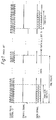
- Fig. 1 there is shown the frame format of a data signal S3, an enable signal S1 and a clock pulse signal S2 for use in a frame synchronization data transmission system.
- one frame is made up of a plurality of subframes, each subframe having 8 bits, each bit being transmitted in synchronization with a clock pulse signal S2.
- each subframe with 8 bits is referred to as an octet or an OCT.
- the enable signal S1 makes logic 1 only when a datum is present.
- a code made up of octadic Os is assigned to the starting octet as the frame synchronizing signal.
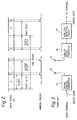
- Fig. 2 shows another frame format, in which there is an octet synchronizing signal.
- the synchronizing signal is assigned to the first bit of each octet and designated with the logic 1.
- the frame synchronizing signal and the subframe synchronizing signal are referred to as the FRM SYN and the SBFRM SYN, respectively, and the two SYNs are referred to in general as the SYN.
- Fig. 3 shows a data transmission system, in which a circuit for detecting an FRM SYN is used.
- the circuit for detecting an FRM SYN is referred to as the FRM SYN detecting circuit.
- a digital data signal sent from a transmitting terminal is converted to an analog data signal by means of digital-analog converter 91.
- the analog data signal is then transmitted through a transmitting antenna 92, received by a receiving antenna 93 and supplied to an analog-digital converter 94 to be converted to a digital data signal.
- An FRM SYN detecting circuit 95 detects an FRM SYN from the digital data signal in order to distinguish whether the digital data signal is a frame of the transmitted data signal, or a data signal which involves any other information, and then sends the digital data signal to a receiving terminal.
- the FRM SYN detecting circuit is provided at the transmitting end as well, in order to enable a check to be made to see if there has been any possible change in the data signal caused by noise.
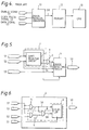
- Fig. 4 shows a block diagram of a typical previously proposed SYN detecting circuit.
- the circuit is composed of a serial-parallel converter 10, a memory 12 and a CPU 13.
- a parallel data signal S11 is first stored in the memory 12. After all of the data signals transmitted by the data transmission system concerned have been stored, the CPU 13 detects the SYN by means of software.
- a problem encountered in the SYN detecting circuit described above is that, since all the serial-to-parallel-converted data have to be stored once in the memory in order to check the bits assigned to the SYN, it takes a long time to detect them.
- an FRM SYN detecting circuit which is capable of effecting detection in real time and which is capable of detecting any error in the frame format in which all bits of the synchronizing signal are designated with codes of an identical logic level.
- a particular SBFRM SYN detecting circuit to be described below includes a starting subframe detecting means both for detecting the starting subframe and for delaying supplied data signal by M clock-pulse periods, the starting subframe detecting means generating a single-pulse signal of the first logic level in synchronization with the kth bit of the second subframe that follows the starting subframe when the starting subframe detecting means does not detect any error in the frame synchronizing signal assigned to the starting subframe, window pulse generating means for generating window pulses, the window pulses being a pulse train with a component pulse generated synchronously with the subframe synchronizing signal of each subframe except for the second subframe, the leading pulse of the pulse train being generated by delaying the single-pulse signal by M clock-pulse periods, the subsequent pulses thereof being recursively generated by delaying the preceding pulse by M clock-pulse periods, and a pulse of the recursively generated pulses that is synchronous with the single-puls
- Figs. 5 and 6 illustrate circuits for detecting a frame synchronizing signal, or an FRM SYN detecting circuit.
- the format of the frame is identical to that illustrated in Fig. 1, the FRM SYN being assigned to the starting octet with each bit designated with logic 0.
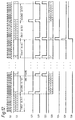
- Fig. 7 an FRM SYN including an error of logic 1 in the third bit is shown.
- the FRM SYN detecting circuit is composed of first-signal generating circuit 1 for providing a first signal S5 and error detecting circuit 4.
- First-signal generating circuit 1 is made up of 8 bit shift register circuit 2 and AND gate 3.
- Shift register circuit 2 receives enable signal S1, shifts it by 8 bits in synchronization with clock pulse signal S2, thereby delaying enable signal S1 by 8 clock-pulse periods.
- AND gate 3 produces a logical product of enable signal S1 and inverted delayed enable signal S4 and delivers the logical product as first signal S5.
- first signal S5 takes a value of logic 1 exclusively while the FRM SYN is received (cf. signal S5 in Fig. 7).
- Error detecting circuit 4 is intended to extract any error present in the FRM SYN.
- Error detecting circuit 4 is provided with AND gate 5 and register circuit 6.
- AND gate 5 receives both first signal S5 and data signal S3 and delivers the logical product as second signal S6, thereby extracting the error bit in the FRM SYN (cf. signal S6 in Fig. 7).
- Register circuit 6 is provided with AND gates 7, 8 and D flip-flop 9.
- AND gate 7 receives both clock pulse signal S2 and first signal S5 and delivers clock pulse train S7 which is active only while the FRM SYN is received (cf. signal S7 in Fig. 7).
- AND gate 8 receives both second signal S6 and clock pulse train S7 and delivers clock pulse S8 which is synchronous with two signals S6, and S7.
- D flip-flop enabled by enable signal S1, receives second signal S6 at its data input and clock pulse S8 at its clock input, latches second signal S6 at the trailing edge of pulse S8 and provides alarm signal S9.
- the FRM SYN detecting circuit can detect any error present in the FRM SYN in real time.
- Figs. 8 to 12 there is shown a circuit for detecting the octet synchronization signal, or an OCT SYN detecting circuit.
- the frame format employed is the same as that represented in Fig. 2.
- the frame is made up of 10 octets.
- the OCT SYN detecting circuit comprises, as seen in Fig. 8, starting subframe detecting circuit 20, window generating circuit 21, transmission gate 22, exclusive-or gate 23 and data converting circuit 24.
- Starting subframe detecting circuit 20 is provided with 8-bit shift register 25 and 8-input NOR gate 26, and the parallel outputs of shift register 25 are connected with the inputs of NOR gate 26, as shown in Fig. 9.
- Shift register 25 shifts data signal S3 in synchronization with clock pulse signal S2.
- the serial output terminal of shift register 25 provides data signal S3 with a delay of 8 clock-pulse periods, which will be referred to as delayed data signal S20 (cf. signal S20 in Fig. 12).
- NOR gate 26 delivers single-pulse signal S21 in synchronization with the OCT SYN of the second octet (the first bit of the second octet) only when it receives logic 0 at all of its eight inputs, i.e., only when starting subframe detecting circuit 20 does not detect any error in the FRM SYN.
- Window pulse generating circuit 21 generates window pulses.
- the window pulses make a pulse train with component pulses generated synchronously with the OCT SYNs (the first bits) of the third and subsequent octets, as shown in Fig. 12 as signal S22.
- Window generating circuit 21 is provided with 8-bit shift register 28, OR gate 29 and exclusive-or gate 30.
- OR gate 29 generates a logical sum of single-pulse signal S21 and the serial output of shift register 28 and delivers it to the serial input of shift register 28 as signal S29.
- Shift register 28 delays serial-input signal S29 by 8 clock-pulse periods and the delayed output or the serial output is again supplied to the serial input via OR gate 29.
- shift register 28 and OR gate 29 cooperate to provide recursive means which generates a pulse train having a single-pulse signal as the leading pulse with a repetition period of 8 clock-pulse periods.
- Exclusive-or gate 30 excludes single-pulse signal S21 from signal S29, thus providing window pulses S22 shown in Fig. 12.
- Transmission gate 22 shown in Fig. 8 transmits delayed data signal S20 under control of window pulse signal, thereby extracting the first bit of the second and subsequent octets assigned to the OCT SYN (delayed by 8 clock-pulse periods)
- the output of transmission gate 22 will be referred to as signal S23.
- Error detecting gate 23 is an exclusive-or gate. It receives window pulses S22 and signal S23 and excludes correct bits assigned to the OCT SYN from being output, thereby delivering any possible error bit S24, as shown in Fig. 12.
- Data converting circuit 24 is provided with serial-parallel converter 30, D flip-flop 32 and AND gate 31.
- Serial-parallel converter 30 converts serially supplied delayed data S20 to parallel data S30 in synchronization with clock pulse signal S2.
- AND gate 31 receives error bit S24 and clock pulse signal S2, and provides clock pulse S31 synchronous with the two inputs.
- D flip-flop 32 latches error bit S24 synchronously with clock pulse S31 and delivers reset signal S32. Reset signal S32 causes serial-parallel converter 30 to be disabled and also causes to generate an alarm signal.
- the FRM SYN is designated by assigning logic 0 to all bits of the starting octets (the first octet) and the OCT SYNs are designated by assigning logic 1 to the first bit in each of the second through tenth octets. Further, it is assumed that the OCT SYN of the tenth octet is in error (logic 0), as shown in data signal S3 in Fig. 12.
- Receiving data signal S3 and clock pulse signal S2, starting subframe detecting circuit 20 delivers single-pulse signal S21 in synchronization with the first bit of the second octets, which indicates the FRM SYN does not include any error.
- Receiving single-pulse signal S21, window pulse generating circuit 21, starting from single-pulse signal repeatedly generates pulses (signal S29) synchronously with the first bit in each octet.
- Exclusive-or gate 30 in window pulse generating circuit 21 shuts out single-pulse signal S21 from signal S29 to provide window pulses S22.
- Window pulses S22 control transmission of delayed data signal 20 through transmission gate 22 to extract the first bits of the second through ninth octets delayed by one octet period (8 clock-pulse periods).
- the exclusive-or gate of error detecting gate 23 excludes correct bits of the first bits delivered from transmission gate 22 from being transmitted and supplies only an error bit to data converting circuit 24.
- Data converting circuit 24 converts normally serial-input delayed data signal S20 to parallel data signal S30. When error bit S24 is detected, data converting circuit 24 stops the serial-parallel conversion and delivers an alarm signal.
- the OCT SYN is assigned to the first bit of each octet.
- the OCT SYN can be assigned to the kth bit (k is larger than 1 and equal to or less than 8).
Landscapes
- Engineering & Computer Science (AREA)
- Computer Networks & Wireless Communication (AREA)
- Signal Processing (AREA)
- Synchronisation In Digital Transmission Systems (AREA)
Applications Claiming Priority (5)
| Application Number | Priority Date | Filing Date | Title |
|---|---|---|---|
| JP22049591 | 1991-08-30 | ||
| JP220495/91 | 1991-08-30 | ||
| JP4142552A JPH05336096A (ja) | 1992-06-03 | 1992-06-03 | フレーム同期信号検出回路 |
| JP142552/92 | 1992-06-03 | ||
| EP92307835A EP0530030B1 (fr) | 1991-08-30 | 1992-08-28 | Circuit pour la détection d'un signal de synchronisation lors de la transmission de données avec synchronisation de trâme |
Related Parent Applications (1)
| Application Number | Title | Priority Date | Filing Date |
|---|---|---|---|
| EP92307835A Division EP0530030B1 (fr) | 1991-08-30 | 1992-08-28 | Circuit pour la détection d'un signal de synchronisation lors de la transmission de données avec synchronisation de trâme |
Publications (1)
| Publication Number | Publication Date |
|---|---|
| EP0880248A1 true EP0880248A1 (fr) | 1998-11-25 |
Family
ID=26474515
Family Applications (2)
| Application Number | Title | Priority Date | Filing Date |
|---|---|---|---|
| EP98201740A Withdrawn EP0880248A1 (fr) | 1991-08-30 | 1992-08-28 | Circuit pour la détection d'un signal de synchronisation lors de la transmission de données avec synchronisation de trâme |
| EP92307835A Expired - Lifetime EP0530030B1 (fr) | 1991-08-30 | 1992-08-28 | Circuit pour la détection d'un signal de synchronisation lors de la transmission de données avec synchronisation de trâme |
Family Applications After (1)
| Application Number | Title | Priority Date | Filing Date |
|---|---|---|---|
| EP92307835A Expired - Lifetime EP0530030B1 (fr) | 1991-08-30 | 1992-08-28 | Circuit pour la détection d'un signal de synchronisation lors de la transmission de données avec synchronisation de trâme |
Country Status (3)
| Country | Link |
|---|---|
| US (1) | US5367543A (fr) |
| EP (2) | EP0880248A1 (fr) |
| DE (1) | DE69227867T2 (fr) |
Families Citing this family (8)
| Publication number | Priority date | Publication date | Assignee | Title |
|---|---|---|---|---|
| US5557616A (en) * | 1992-04-02 | 1996-09-17 | Applied Digital Access, Inc. | Frame synchronization in a performance monitoring and test system |
| SE501156C2 (sv) * | 1993-04-21 | 1994-11-28 | Ellemtel Utvecklings Ab | Referenssignal sammansatt av klocksignal och synkroniseringssignal, anordning och förfarande för synkronisering m.h.a. referenssignal |
| DE4429595C1 (de) * | 1994-08-20 | 1995-06-29 | Philips Patentverwaltung | Übertragungssystem zur Übertragung und zur Erkennung des Rahmenanfangs eines rahmensynchronisierten Signals |
| JP3048504B2 (ja) * | 1994-09-26 | 2000-06-05 | 沖電気工業株式会社 | 信号検出回路及びフレーム同期回路 |
| JP2944440B2 (ja) * | 1994-12-27 | 1999-09-06 | 日本電気株式会社 | 時分割多重伝送装置 |
| JP3493111B2 (ja) * | 1997-02-25 | 2004-02-03 | 株式会社東芝 | 半導体集積回路装置 |
| US6611538B1 (en) | 1999-05-27 | 2003-08-26 | 3Com Corporation | Data transmission synchronization system |
| US6658363B2 (en) * | 2001-01-18 | 2003-12-02 | Hewlett-Packard Development Company, L.P. | Digital data pattern detection methods and arrangements |
Citations (3)
| Publication number | Priority date | Publication date | Assignee | Title |
|---|---|---|---|---|
| US3594502A (en) * | 1968-12-04 | 1971-07-20 | Itt | A rapid frame synchronization system |
| DE3013554A1 (de) * | 1979-04-10 | 1980-10-16 | Mitsubishi Electric Corp | Digitales signaluebertragungssystem |
| DE3132198A1 (de) * | 1981-08-14 | 1983-03-03 | TE KA DE Felten & Guilleaume Fernmeldeanlagen GmbH, 8500 Nürnberg | Verfahren und schaltungsanordnung zur synchronisation von datensignalen |
Family Cites Families (8)
| Publication number | Priority date | Publication date | Assignee | Title |
|---|---|---|---|---|
| GB964901A (en) * | 1960-02-12 | 1964-07-29 | Nippon Electric Co | A synchronising system for a time division multiplex pulse code modulation system |
| US3472961A (en) * | 1966-02-28 | 1969-10-14 | Xerox Corp | Synchronization monitor apparatus |
| US4247936A (en) * | 1979-06-06 | 1981-01-27 | Minnesota Mining And Manufacturing Company | Digital communications system with automatic frame synchronization and detector circuitry |
| JPS59221047A (ja) * | 1983-05-30 | 1984-12-12 | Victor Co Of Japan Ltd | デイジタル信号伝送における同期信号検出回路 |
| AU585794B2 (en) * | 1986-01-09 | 1989-06-22 | Nec Corporation | Frame synchronization detection system |
| CA1266515A (fr) * | 1986-09-04 | 1990-03-06 | Nec Corporation | Appareil de detection de configuration de debut |
| DE3722567A1 (de) * | 1987-07-08 | 1989-01-19 | Siemens Ag | Verfahren und schaltungsanordnung zur rahmensynchronisierung |
| US5228037A (en) * | 1990-03-27 | 1993-07-13 | Nec Corporation | Line interface for high-speed line |
-
1992
- 1992-08-28 EP EP98201740A patent/EP0880248A1/fr not_active Withdrawn
- 1992-08-28 DE DE69227867T patent/DE69227867T2/de not_active Expired - Fee Related
- 1992-08-28 EP EP92307835A patent/EP0530030B1/fr not_active Expired - Lifetime
- 1992-08-31 US US07/938,411 patent/US5367543A/en not_active Expired - Fee Related
Patent Citations (3)
| Publication number | Priority date | Publication date | Assignee | Title |
|---|---|---|---|---|
| US3594502A (en) * | 1968-12-04 | 1971-07-20 | Itt | A rapid frame synchronization system |
| DE3013554A1 (de) * | 1979-04-10 | 1980-10-16 | Mitsubishi Electric Corp | Digitales signaluebertragungssystem |
| DE3132198A1 (de) * | 1981-08-14 | 1983-03-03 | TE KA DE Felten & Guilleaume Fernmeldeanlagen GmbH, 8500 Nürnberg | Verfahren und schaltungsanordnung zur synchronisation von datensignalen |
Non-Patent Citations (1)
| Title |
|---|
| H. MIYAKAWA ET AL.: "Methodsof Construction of Comma-Free Codes with Fixed Block Sync Pattern", ELECTRONICS AND COMMUNICATIONS IN JAPAN, vol. 52-A, no. 5, May 1969 (1969-05-01), NEW YORK US, pages 10 - 16, XP002078137 * |
Also Published As
| Publication number | Publication date |
|---|---|
| DE69227867T2 (de) | 1999-05-27 |
| EP0530030B1 (fr) | 1998-12-16 |
| EP0530030A3 (en) | 1994-08-17 |
| US5367543A (en) | 1994-11-22 |
| DE69227867D1 (de) | 1999-01-28 |
| EP0530030A2 (fr) | 1993-03-03 |
Similar Documents
| Publication | Publication Date | Title |
|---|---|---|
| EP0773653A2 (fr) | Procédé et appareil de décodage de données codées en code Manchester | |
| EP0090019B1 (fr) | Circuit de detection d'erreurs dans des communications codees par signaux d'horloge de sources multiples | |
| JPS63296425A (ja) | 通信方法及び符号化装置 | |
| US6795515B1 (en) | Method and apparatus for locating sampling points in a synchronous data stream | |
| US5367543A (en) | Circuit for detecting synchronizing signal in frame synchronization data transmission | |
| EP0265080B1 (fr) | Dispositif pour la détection de la difference de bit-phase | |
| US6985546B2 (en) | Transmitting circuit and method thereof, receiving circuit and method thereof, and data communication apparatus | |
| US6977973B1 (en) | System and method for decoding manchester data | |
| US5627828A (en) | Method and circuit for detecting data collisions in communication network | |
| US4675545A (en) | Wave shaping apparatus for eliminating pulse width distortion | |
| JP2003134098A (ja) | シリアル受信装置 | |
| US5525974A (en) | Radio selective calling receiver for receiving a call signal intermittently under an asynchronous system | |
| US6996201B2 (en) | Data receiving system robust against jitter of clock | |
| RU2239953C2 (ru) | Устройство для синхронизации по циклам | |
| US4464769A (en) | Method and apparatus for synchronizing a binary data signal | |
| RU2231228C1 (ru) | Устройство для синхронизации по циклам | |
| US6970527B2 (en) | Transmitting circuit and method thereof, receiving circuit and method thereof, and data communication apparatus | |
| JP2973725B2 (ja) | サブフレーム同期信号検出回路 | |
| US6307904B1 (en) | Clock recovery circuit | |
| EP0479607A2 (fr) | Méthode et appareil de détection d'une séquence au bits de trame dans un système numérique de transmission de données | |
| JP2857852B2 (ja) | フレーム同期コード検出回路 | |
| JP3001414B2 (ja) | 符号誤り訂正装置 | |
| JP3279869B2 (ja) | Ami符号受信回路 | |
| JP4227860B2 (ja) | リセット回路 | |
| JP2000295193A (ja) | 同期検出装置 |
Legal Events
| Date | Code | Title | Description |
|---|---|---|---|
| PUAI | Public reference made under article 153(3) epc to a published international application that has entered the european phase |
Free format text: ORIGINAL CODE: 0009012 |
|
| 17P | Request for examination filed |
Effective date: 19980609 |
|
| AC | Divisional application: reference to earlier application |
Ref document number: 530030 Country of ref document: EP |
|
| AK | Designated contracting states |
Kind code of ref document: A1 Designated state(s): DE FR GB SE |
|
| STAA | Information on the status of an ep patent application or granted ep patent |
Free format text: STATUS: THE APPLICATION IS DEEMED TO BE WITHDRAWN |
|
| 18D | Application deemed to be withdrawn |
Effective date: 20020301 |