EP0880309A2 - Réduction du bruit électromagnétique émis par un panneau à circuit imprimé - Google Patents
Réduction du bruit électromagnétique émis par un panneau à circuit imprimé Download PDFInfo
- Publication number
- EP0880309A2 EP0880309A2 EP98108818A EP98108818A EP0880309A2 EP 0880309 A2 EP0880309 A2 EP 0880309A2 EP 98108818 A EP98108818 A EP 98108818A EP 98108818 A EP98108818 A EP 98108818A EP 0880309 A2 EP0880309 A2 EP 0880309A2
- Authority
- EP
- European Patent Office
- Prior art keywords
- power supply
- layers
- printed board
- ground
- spiral coil
- Prior art date
- Legal status (The legal status is an assumption and is not a legal conclusion. Google has not performed a legal analysis and makes no representation as to the accuracy of the status listed.)
- Withdrawn
Links
Images



Classifications
-
- H—ELECTRICITY
- H05—ELECTRIC TECHNIQUES NOT OTHERWISE PROVIDED FOR
- H05K—PRINTED CIRCUITS; CASINGS OR CONSTRUCTIONAL DETAILS OF ELECTRIC APPARATUS; MANUFACTURE OF ASSEMBLAGES OF ELECTRICAL COMPONENTS
- H05K1/00—Printed circuits
- H05K1/16—Printed circuits incorporating printed electric components, e.g. printed resistors, capacitors or inductors
- H05K1/162—Printed circuits incorporating printed electric components, e.g. printed resistors, capacitors or inductors incorporating printed capacitors
-
- H—ELECTRICITY
- H05—ELECTRIC TECHNIQUES NOT OTHERWISE PROVIDED FOR
- H05K—PRINTED CIRCUITS; CASINGS OR CONSTRUCTIONAL DETAILS OF ELECTRIC APPARATUS; MANUFACTURE OF ASSEMBLAGES OF ELECTRICAL COMPONENTS
- H05K1/00—Printed circuits
- H05K1/16—Printed circuits incorporating printed electric components, e.g. printed resistors, capacitors or inductors
- H05K1/165—Printed circuits incorporating printed electric components, e.g. printed resistors, capacitors or inductors incorporating printed inductors
-
- H—ELECTRICITY
- H05—ELECTRIC TECHNIQUES NOT OTHERWISE PROVIDED FOR
- H05K—PRINTED CIRCUITS; CASINGS OR CONSTRUCTIONAL DETAILS OF ELECTRIC APPARATUS; MANUFACTURE OF ASSEMBLAGES OF ELECTRICAL COMPONENTS
- H05K1/00—Printed circuits
- H05K1/02—Details
- H05K1/0213—Electrical arrangements not otherwise provided for
- H05K1/0216—Reduction of cross-talk, noise or electromagnetic interference
-
- H—ELECTRICITY
- H05—ELECTRIC TECHNIQUES NOT OTHERWISE PROVIDED FOR
- H05K—PRINTED CIRCUITS; CASINGS OR CONSTRUCTIONAL DETAILS OF ELECTRIC APPARATUS; MANUFACTURE OF ASSEMBLAGES OF ELECTRICAL COMPONENTS
- H05K1/00—Printed circuits
- H05K1/02—Details
- H05K1/0213—Electrical arrangements not otherwise provided for
- H05K1/0216—Reduction of cross-talk, noise or electromagnetic interference
- H05K1/023—Reduction of cross-talk, noise or electromagnetic interference using auxiliary mounted passive components or auxiliary substances
- H05K1/0233—Filters, inductors or a magnetic substance
-
- H—ELECTRICITY
- H05—ELECTRIC TECHNIQUES NOT OTHERWISE PROVIDED FOR
- H05K—PRINTED CIRCUITS; CASINGS OR CONSTRUCTIONAL DETAILS OF ELECTRIC APPARATUS; MANUFACTURE OF ASSEMBLAGES OF ELECTRICAL COMPONENTS
- H05K1/00—Printed circuits
- H05K1/02—Details
- H05K1/11—Printed elements for providing electric connections to or between printed circuits
- H05K1/115—Via connections; Lands around holes or via connections
-
- H—ELECTRICITY
- H05—ELECTRIC TECHNIQUES NOT OTHERWISE PROVIDED FOR
- H05K—PRINTED CIRCUITS; CASINGS OR CONSTRUCTIONAL DETAILS OF ELECTRIC APPARATUS; MANUFACTURE OF ASSEMBLAGES OF ELECTRICAL COMPONENTS
- H05K1/00—Printed circuits
- H05K1/02—Details
- H05K1/0213—Electrical arrangements not otherwise provided for
- H05K1/0216—Reduction of cross-talk, noise or electromagnetic interference
- H05K1/023—Reduction of cross-talk, noise or electromagnetic interference using auxiliary mounted passive components or auxiliary substances
- H05K1/0231—Capacitors or dielectric substances
-
- H—ELECTRICITY
- H05—ELECTRIC TECHNIQUES NOT OTHERWISE PROVIDED FOR
- H05K—PRINTED CIRCUITS; CASINGS OR CONSTRUCTIONAL DETAILS OF ELECTRIC APPARATUS; MANUFACTURE OF ASSEMBLAGES OF ELECTRICAL COMPONENTS
- H05K2201/00—Indexing scheme relating to printed circuits covered by H05K1/00
- H05K2201/08—Magnetic details
- H05K2201/083—Magnetic materials
- H05K2201/086—Magnetic materials for inductive purposes, e.g. printed inductor with ferrite core
-
- H—ELECTRICITY
- H05—ELECTRIC TECHNIQUES NOT OTHERWISE PROVIDED FOR
- H05K—PRINTED CIRCUITS; CASINGS OR CONSTRUCTIONAL DETAILS OF ELECTRIC APPARATUS; MANUFACTURE OF ASSEMBLAGES OF ELECTRICAL COMPONENTS
- H05K2201/00—Indexing scheme relating to printed circuits covered by H05K1/00
- H05K2201/09—Shape and layout
- H05K2201/09209—Shape and layout details of conductors
- H05K2201/0929—Conductive planes
- H05K2201/09309—Core having two or more power planes; Capacitive laminate of two power planes
-
- H—ELECTRICITY
- H05—ELECTRIC TECHNIQUES NOT OTHERWISE PROVIDED FOR
- H05K—PRINTED CIRCUITS; CASINGS OR CONSTRUCTIONAL DETAILS OF ELECTRIC APPARATUS; MANUFACTURE OF ASSEMBLAGES OF ELECTRICAL COMPONENTS
- H05K2201/00—Indexing scheme relating to printed circuits covered by H05K1/00
- H05K2201/09—Shape and layout
- H05K2201/09209—Shape and layout details of conductors
- H05K2201/0929—Conductive planes
- H05K2201/09336—Signal conductors in same plane as power plane
-
- H—ELECTRICITY
- H05—ELECTRIC TECHNIQUES NOT OTHERWISE PROVIDED FOR
- H05K—PRINTED CIRCUITS; CASINGS OR CONSTRUCTIONAL DETAILS OF ELECTRIC APPARATUS; MANUFACTURE OF ASSEMBLAGES OF ELECTRICAL COMPONENTS
- H05K2201/00—Indexing scheme relating to printed circuits covered by H05K1/00
- H05K2201/09—Shape and layout
- H05K2201/09209—Shape and layout details of conductors
- H05K2201/09654—Shape and layout details of conductors covering at least two types of conductors provided for in H05K2201/09218 - H05K2201/095
- H05K2201/097—Alternating conductors, e.g. alternating different shaped pads, twisted pairs; Alternating components
-
- H—ELECTRICITY
- H05—ELECTRIC TECHNIQUES NOT OTHERWISE PROVIDED FOR
- H05K—PRINTED CIRCUITS; CASINGS OR CONSTRUCTIONAL DETAILS OF ELECTRIC APPARATUS; MANUFACTURE OF ASSEMBLAGES OF ELECTRICAL COMPONENTS
- H05K2201/00—Indexing scheme relating to printed circuits covered by H05K1/00
- H05K2201/10—Details of components or other objects attached to or integrated in a printed circuit board
- H05K2201/10007—Types of components
- H05K2201/1003—Non-printed inductor
-
- H—ELECTRICITY
- H05—ELECTRIC TECHNIQUES NOT OTHERWISE PROVIDED FOR
- H05K—PRINTED CIRCUITS; CASINGS OR CONSTRUCTIONAL DETAILS OF ELECTRIC APPARATUS; MANUFACTURE OF ASSEMBLAGES OF ELECTRICAL COMPONENTS
- H05K3/00—Apparatus or processes for manufacturing printed circuits
- H05K3/46—Manufacturing multilayer circuits
- H05K3/4688—Composite multilayer circuits, i.e. comprising insulating layers having different properties
Definitions
- the present invention relates to a printed board which supports circuit devices including transistors, ICs (Integrated Circuits), LSI (Large Scale Integration) circuits, etc.
- Printed boards support circuit devices including transistors, ICs, LSI circuits, etc. suffer conductive or radiant electromagnetic noise due to high-frequency currents generated by the circuit devices and circulating currents known as a common-mode signal flowing through parasitic capacitances and parasitic mutual inductances which circuits on the printed boards have. When electromagnetic noise is generated, it tends to cause an error in electronic units which incorporate such printed boards or other electronic units.
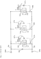
- the conventional printed board supports circuit devices 101, 102, 103 for generating high-frequency currents whose magnitudes are different from each other, the circuit devices 101, 102, 103 being connected parallel to each other between a power supply line 104 and a ground line 105.
- the circuit device 101 generates a high-frequency current whose magnitude is the greatest
- the circuit device 102 generates a high-frequency current whose magnitude is the second greatest
- the circuit device 103 generates a high-frequency current whose magnitude is the third greatest.
- the power supply line 104 is formed in a power supply layer (not shown) of the printed board, and the ground line 105 in a ground layer (not shown) of the printed board.
- the power supply layer is disposed as a planar layer which comprises an electrically conductive layer formed over the entire surface of the printed board.
- the printed board is supplied with electric energy from a power supply which is connected to a power supply terminal 104a of the power supply line 104 and a power supply ground terminal 105a of the ground line 105.
- a decoupling capacitor 106 is connected between the power supply line 104 and the ground line 105 near the power supply terminal 104a and the power supply ground terminal 105a.
- Decoupling capacitors 107a, 107b, 107c which have respective capacitances commensurate with the magnitudes of the high-frequency currents generated by the respective circuit devices 101, 102, 103, are connected across the respective circuit devices 101, 102, 103 between power supply terminals 101a, 102a, 103a and ground terminals 101b, 102b, 103b of the respective circuit devices 101, 102, 103.
- the decoupling capacitor 107a has an electrostatic capacitance whose magnitude is the greatest
- the decoupling capacitor 107b has an electrostatic capacitance whose magnitude is the second greatest
- the decoupling capacitor 107c has an electrostatic capacitance whose magnitude is the third greatest.
- the decoupling capacitor 107c Since the impedances of the decoupling capacitors 107a, 107b, 107c are inversely proportional to the magnitudes of their electrostatic capacitances, the decoupling capacitor 107c has an impedance whose magnitude is the greatest, the decoupling capacitor 107b has an impedance whose magnitude is the second greatest, and the decoupling capacitor 107a has an impedance whose magnitude is the third greatest.
- the high-frequency currents generated by the circuit devices 101, 102, 103 flow respectively through the decoupling capacitors 107a, 107b, 107c to the ground line 105, so that the voltages at the power supply terminals 101a, 102a, 103a of the circuit devices 101, 102, 103 are prevented from varying.
- the resistance, i.e., the impedance, of the power supply line 104 is small. Consequently, the voltage at the power supply layer is also prevented from varying even when high-frequency currents flow into the power supply line 104.
- the impedance of the power supply layer is smaller than the impedances of the decoupling capacitors 107a, 107b, 107c. Therefore, the high-frequency currents generated by the circuit devices 101, 102, 103 may not flow through the decoupling capacitors 107a, 107b, 107c, but may flow through the power supply layer into other circuit devices or decoupling capacitors which have smaller impedances or larger electrostatic capacitances.
- decoupling capacitors 107a, 107b, 107c have different impedance vs. frequency characteristics depending on the electrostatic capacitance even if they are of the same type. For example, the impedance of a decoupling capacitor having a smaller electrostatic capacitance tends to be smaller than the impedance of a decoupling capacitor having a larger electrostatic capacitance at frequencies higher than a certain frequency. Consequently, high-frequency currents whose frequencies reside in a wide frequency band flow into and out of the decoupling capacitors. For this reason, printed boards need to be fitted with many capacitors whose electrostatic capacitances are much greater than the electrostatic capacitances that are theoretically required.
- the high-frequency current When a high-frequency current flows into the planar power supply layer, the high-frequency current may act as a loop current in the power supply layer, or a common-mode high-frequency current may flow into a cable connected to the printed board, resulting in the radiation of electromagnetic noise. If a high-frequency current generated by a circuit device does not flow into a decoupling capacitor connected thereacross, but flows into another path, then the impedance of the path is increased, causing a large voltage variation in another circuit device, whose stable operation will adversely be affected.
- An electronic unit which comprises a plurality of such printed boards is housed in a metallic casing for preventing electromagnetic noise from leaking out. Cables connected to the electronic unit and extending out of the casing are fitted with common-mode coils and cores for suppressing the conduction of electromagnetic noise.
- common-mode coils and cores for suppressing the conduction of electromagnetic noise.
- Japanese laid-open patent publication No. 300593/88 discloses laminating a magnetic sheet to a coil pattern to form an inductor for thereby increasing the inductance.
- a magnetic layer is disposed on a first conductor layer, and covered with a second conductor layer, making up an inductive device.
- Japanese laid-open patent publications Nos. 273699/91 and 293416/96 show the formation of a coil-shaped inductor by successively connecting printed interconnections on two superposed conductor layers via through holes.
- a printed board has at least two conductor layers including a power supply layer and a ground layer, and a spiral coil inductor disposed in opposite ones of the conductor layers.
- the spiral coil inductor has a terminal connected to a power supply line of the power supply layer, and another terminal connected to a device power terminal disposed on one of the conductor layers and to be connected to a power supply terminal of a circuit device and a terminal of a decoupling capacitor.
- a device ground terminal is disposed on one of the conductor layers and to be connected to a ground terminal of the circuit device and another terminal of the decoupling capacitor, the device ground terminal being connected to a ground line of the ground layer.
- a high-frequency current generated by the circuit device flows through the decoupling capacitor to the ground layer. As a result, electromagnetic noise radiated from the printed board is reduced.
- the spiral coil inductor may comprise a toroidal spiral coil inductor for thereby increasing the impedance between the power supply line and the circuit device even though only a limited area is available for installing the spiral coil inductor.
- the opposite ones of the conductor layers may comprise the power supply layer and the ground layer, respectively. Since conductor lines of the spiral coil inductors are formed by defining frame-like recesses in the conductor layers, the conductor lines are insulated from and electrically independent of the conductor layers. Accordingly, the spiral coil inductors may be disposed between any two opposite conductor layers. Even if the conductor layers comprise only power supply and ground layers, other conductor layers do not need to be added for providing the spiral coil inductor.
- the conductor layers may comprise two opposite power supply layers and two ground layers disposed respectively on surfaces of the two opposite power supply layers, and the conductor lines of the spiral coil inductor may be disposed on the two opposite power supply layers.
- the spiral coil inductors disposed between the power supply layers are sandwiched by the ground layers, and hence provide stable characteristics.
- the ground layers serve as a shield for reducing the effect of a magnetic field generated by the toroidal spiral coil inductors on the signal layers.
- the conductor layers may further comprise two signal layers disposed respectively on surfaces of the ground layers, the through holes or via holes including through holes or via holes extending through the power supply layers and the ground layers and interconnecting the signal layers and through holes or via holes extending through the power supply layers and interconnecting the ground layers, the through holes or via holes being disposed closely to each other, lowering the impedance between the signal layers and the ground layers.
- the lowered impedance between the signal layers and the ground layers reduces electromagnetic noise induced by signal currents flowing through the through holes or via holes and minimizes distortions of the signal waveform.
- the printed board further comprises an insulating layer disposed between the opposite ones of the conductor layers, the insulating layer containing a magnetic material.
- the insulating layer mixed with a magnetic material functions as the magnetic core of the spiral coil inductors, so that the inductance of the spiral coil inductors increases.
- the insulating layer may be disposed in a coil interior surrounded by at least the conductor lines of the spiral coil inductor and the through holes or via holes.
- the insulating layer mixed with a magnetic material also functions as the magnetic core of the spiral coil inductors
- the insulating layer may comprise an insulating solvent mixed with a fine powder of Ni - Zn ferrite as the magnetic material, or an insulating solvent mixed with a fine powder of Mn - Zn ferrite as the magnetic material, or an insulating solvent mixed with a fine powder of Li ferrite as the magnetic material, or an insulating solvent mixed with a fine powder of Sendust as the magnetic material, or an insulating solvent mixed with a fine powder of amorphous material as the magnetic material, or an insulating solvent mixed with a fine powder of Permalloy as the magnetic material.
- the insulating layer may comprise an amorphous material foil having opposite surfaces each coated with an insulating coating.
- a printed board comprises at least two conductor layers and a toroidal spiral coil inductor comprising a plurality of conductor lines defined by frame-like recesses defined in opposite ones of the conductor layers, and through holes or via holes interconnecting the conductor lines. Since the toroidal spiral coil inductor has a longer coil average magnetic path than a spiral coil inductor, the inductance of the inductor on the printed board increases.
- a printed board 1 has a power supply layer 3 disposed on an upper surface of an insulating layer 2 and a ground layer 4 disposed on a lower surface of the insulating layer 2.
- Each of the power supply layer 3 and the ground layer 4 serves as a conductor layer and is formed of an electrically conductive material such as copper foil or the like.
- the power supply layer 3 comprises a power supply line 9 having a power supply terminal (not shown) for connection to a power supply (not shown), and the ground layer 4 comprises a ground line 13 having a power supply ground terminal (not shown) for connection to the power supply.
- Circuit devices including transistors, ICs, LSI circuits, etc. mounted on the printed board 1 each have a power supply terminal (not shown) and a ground terminal (not shown).
- the power supply terminals of the circuit devices are to be connected to device power terminals 3a (see Fig.5) of the power supply layer 3, and the ground terminals of the circuit devices are to be connected to device ground terminals 4a (see Fig.5) of the ground layer 4.
- the device ground terminals 4a are connected to the ground line 13.
- Decoupling capacitors (not shown) are to be connected between the device power terminals 3a and the device ground terminals 4a.
- a decoupling capacitor is also to be connected between the power supply line 9 and the ground line 13 near the power supply terminal and the power supply ground
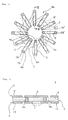
- Frame-like recesses are defined in the power supply layer 3, leaving a plurality of conductor lines 5 in the power supply layer 3.
- the conductor lines 5 are disposed at equal angular intervals in a radial pattern around a certain central point.
- the conductor lines 5 are shown parallel to each other for illustrative purpose.
- Each of the conductor lines 5 has through holes 6a, 6b defined respectively in radially inner and outer ends 5a, 5b thereof, the through holes 6a, 6b extending and connected to the ground layer 4 (see Fig. 3).
- the power supply line 9 and the ground line 13 are omitted from illustration.
- each of the conductor lines 7 has a radially inner end 7a connected to the through hole 6a defined in the radially inner end 5a of one of the conductor lines 5, and a radially outer end 7b connected to the radially outer end 5b of an adjacent one of the conductor lines 5.
- One of the conductor lines 5 has a radially outer end 5b' connected to the power supply terminal of the power supply layer 3 (see Fig. 3), and one of the conductor lines 7 has a radially outer end 7b' connected to one of the device power terminals of the power supply layer 3.
- No through hole is defined between the radially outer end 5b' and the radially outer end 7b'.
- the conductor lines 5, 7 and the through holes 6a, 6b jointly make up a toroidal spiral coil inductor 8a (see Fig. 2) disposed between the power supply layer 3 and the ground layer 4, i.e., within the printed board 1.
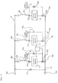
- the printed board according to the first embodiment has a plurality of toroidal spiral coil inductors 8a, 8b, 8c, each identical to the toroidal spiral coil inductor 8a shown in Fig. 2, connected between a power supply line 9 and respective device power terminals 3a of the power supply layer 3 (see Fig. 3).
- Circuit devices 10, 11, 12 have respective power supply terminals 10a, 10b, 10c connected respectively to the device power terminals 3a, and respective ground terminals 10b, 11b, 12b connected respectively to device ground terminals 4a of the ground line 13 (see Fig. 3).
- Decoupling capacitors 15a, 15b, 15c are connected across the respective circuit devices 10, 11, 12 between the device power terminals 3a and the device ground terminals 4a, thus making up decoupling circuits associated respectively with the circuit devices 10, 11, 12.
- a high-frequency filter 16 comprising a toroidal spiral coil inductor is connected between the circuit devices 10, 11.
- the toroidal spiral coil inductors 8a, 8b, 8c have respective capacitances depending on the magnitudes of high-frequency currents generated respectively by the circuit devices 10, 11, 12.
- the power supply line 9 has a power supply terminal 9a
- the ground line 13 has a power supply ground terminal 13a.
- a decoupling capacitor 14 is to be connected between the power supply line 9 and the ground line 13 near the power supply terminal 9a and the power supply ground terminal 13a.
- a power supply (not shown) is to be connected to the power supply terminal 9a and the power supply ground terminal 13a.
- the power supply terminal 9a, the power supply ground terminal 13a, the decoupling capacitor 14, and the power supply are identical to those described with respect to the conventional printed board shown in Fig. 1, and will not be described in detail below.
- the printed board according to the first embodiment may support as many circuit devices as desired, not just three circuit devices as illustrated, and those circuit devices are associated with respective decoupling circuits.
- the toroidal spiral coil inductor as a high-frequency filter 16 may be connected between other circuit devices as well as between the circuit devices 10, 11.
- the through holes 6a, 6b and other through holes described later on may be replaced with via holes.
- Fig. 6 shows in perspective a connected structure of one of the decoupling circuits of the printed board shown in Fig. 5.
- the toroidal spiral coil inductor 8a has a terminal connected to the power supply line 9 of the power supply layer 3 and another terminal connected to the power supply terminal 10a of the circuit device 10.
- the decoupling capacitor 15a has a terminal connected to the power supply terminal 10a and another terminal connected to the ground line 13 of the ground layer 4.
- the ground terminal 10b of the circuit device 10 is connected to the ground line 13.
- the toroidal spiral coil inductors 8a, 8b, 8c provide large impedances between the power supply line 9 and the circuit devices 10, 11, 12. Therefore, high-frequency currents generated by the circuit devices 10, 11, 12 do not flow through the power supply line 9, but flow through the decoupling capacitors 15a, 15b, 15c to the ground line 13. Consequently, the high-frequency currents generated by the circuit devices 10, 11, 12 are less likely to flow through the power supply layer 3 into the circuit devices 10, 11, 12 and the decoupling capacitors 15a, 15b, 15c.
- the decoupling capacitors 15a, 15b, 15c are supplied with only the high-frequency currents generated by the circuit devices 10, 11, 12 positioned closely to the decoupling capacitors 15a, 15b, 15c, the magnitudes of the high-frequency currents are able to be grasped, it is possible to determine the electrostatic capacitances of the decoupling capacitors 15a, 15b, 15c with accuracy. Inasmuch as high-frequency currents flowing into the power supply layer 3 are suppressed, no appreciable loop current is produced in the power supply layer 3, so that no electromagnetic noise will be radiated and noise immunity is prevented from being impaired. Because high-frequency currents generated by the circuit devices 10, 11, 12 are prevented from flowing into the other circuit devices 10, 11, 12, voltage variations in the circuit devices 10, 11, 12 are suppressed, and hence the circuit devices 10, 11, 12 can operate more stably.
- the power supply layer 3 which provides the power supply line 9 is formed as a planar layer except the conductor lines 5, the power supply line 9 has a relatively small resistance, and hence voltage variations in the power supply line 9 are suppressed. Any voltage variations in the circuit devices 10, 11, 12 can be minimized when the resistances of the toroidal spiral coil inductors 8a, 8b, 8c are minimized by selecting the length and width of the conductor lines 5, 7 of the toroidal spiral coil inductors 8a, 8b, 8c.
- the toroidal spiral coil inductor connected as a high-frequency 16 filter between the circuit devices 10, 11 tends to reduce the rate at which a rectangular-wave signal rises or falls in the circuit devices 10, 11 even if the circuit devices 10, 11 comprise high-speed processing ICs or LSI circuits. Therefore, the printed board is less subject to conductive or radiant electromagnetic noise which would otherwise occur if a rectangular-wave signal rises or falls too fast in the circuit devices 10, 11.
- the toroidal spiral coil inductors 8a, 8b, 8c, 8d are disposed between the power supply layer 3 and the ground layer 4 within the printed board 1. Since no inductors need to be separately mounted on the printed board 1, the printed board 1 provides a wider interconnection area thereon. Even though spaces are limited for installing the toroidal spiral coil inductors 8a, 8b, 8c therein, the toroidal spiral coil inductors 8a, 8b, 8c are effective in increasing the impedance between the power supply line 9 and the circuit devices 10, 11, 12.
- the decoupling circuit shown in Fig. 6 it is preferable to make as short as possible the path from the power supply terminal 10a through the decoupling capacitor 15a to the ground line 13. Since this is effective to reduce the resistance through the decoupling capacitor 15a, the high-frequency current generated by the circuit device 10 finds it easier to flow through the decoupling capacitor 15a.
- a plurality of conductor lines 25 of a power supply layer and a plurality of conductor lines 27 of a ground layer are disposed in a superimposed zigzag pattern in a printed board 21.
- the conductor lines 25, 27 have ends interconnected by through holes 26.
- the conductor lines 25, 27 and the through holes 26 jointly provide a non-toroidal spiral coil inductor 28 between the power supply layer and the ground layer of the printed board 21.
- the inductance of the spiral coil inductor is proportional to the square of the number of turns of the spiral coil, and is greater as the average magnetic path length is greater.
- the average magnetic path length of the non-toroidal spiral coil inductor 28 is represented by a closed curve 28a extending between radially outer and inner ends of the spiral coil.
- the closed curve 28a extending near the radially outer end of the spiral coil may not necessarily be uniform and shortest in length.
- the toroidal spiral coil inductor 8a shown in Fig. 2 has an average magnetic path length represented by a closed curve 8' which is uniform and shortest in length. Therefore, the toroidal spiral coil inductor provides a greater inductance.
- Fig. 8 shows in cross section a first modification of the printed board shown in Figs. 2 through 6.
- a printed board 31 according to the first modification has a power supply layer 33 disposed on an upper surface of a first insulating layer 32a and a ground layer 34 disposed on a lower surface of the first insulating layer 32a.
- Second insulating layers 32b are disposed respectively on outer surfaces of the power supply layer 33 and the ground layer 34.
- Signal layers 35 having interconnections for transmitting signals are disposed respectively on outer surfaces of the second insulating layers 32b.
- Toroidal spiral coil inductors (not shown) are disposed between the power supply layer 33 and the ground layer 34.
- Conductor lines and through holes (not shown) of the toroidal spiral coil inductors, the power supply layer 33, the ground layer 34, circuit devices (not shown) which are to be connected to the printed board 31, and decoupling capacitors (not shown) are identical to those of the printed board shown in Figs. 2 through 5, and will not be described in detail below.
- the device power terminals are disposed on the power layer, and the device ground terminals are disposed on the ground layer.
- the device power terminals and the device ground terminals may be disposed on any of these conductor layers.
- the toroidal spiral coil inductors are disposed between the power supply layer 33 and the ground layer 34, i.e., within the printed board 31. Therefore, the toroidal spiral coil inductors may be disposed in a printed circuit having two or more conductor layers as shown in Fig. 8. Since conductor lines of the toroidal spiral coil inductors are formed by defining frame-like recesses in the conductor layers, the conductor lined are insulated from and electrically independent of the conductor layers. Accordingly, the conductor lines may not necessarily be formed in the power supply layer 33 and the ground layer 34, but may be formed in the signal layers 35. Consequently, the toroidal spiral coil inductors may be disposed between any two opposite conductor layers, e.g., between the power supply layer 33 and the opposite signal layer 35 or between the ground line 34 and the opposite signal layer 35.
- Fig. 9 shows in cross section a second modification of the printed board shown in Figs. 2 through 6.
- a printed board 41 according to the second modification has two power supply layers 43 disposed on respective surfaces of a first insulating layer 42a, two second insulating layers 42b disposed on respective outer surfaces of the power supply layers 43, and two ground layers 44 disposed on respective outer surfaces of the second insulating layers 42b.
- Third insulating layers 42c are disposed respectively on outer surfaces of the ground layers 44, and signal layers 45 are disposed respectively on outer surfaces of the third insulating layers 42c.
- Toroidal spiral coil inductors (not shown) are disposed between the two power supply layers 43.
- Conductor lines and through holes (not shown) of the toroidal spiral coil inductors, the power supply layers 43, the ground layers 44, device power terminals (not shown), device ground terminals (not shown), circuit devices (not shown) which are to be connected to the printed board 41, and decoupling capacitors (not shown) are identical to those of the printed board shown in Figs. 2 through 5, and will not be described in detail below.
- the device power terminals are disposed on the power layer, and the device ground terminals are disposed on the ground layer.
- the device power terminals and the device ground terminals may be disposed on any of these conductor layers.
- the toroidal spiral coil inductors disposed between the power supply layers 43 are sandwiched by the ground layers 44, and hence provide stable characteristics.
- the ground layers 44 serve as a shield for reducing the effect of a magnetic field generated by the toroidal spiral coil inductors on the signal layers 45.
- the conductor lines of the power supply layers 43 and the ground layers 44 which face those conductor lines are electrostatically coupled to reduce the impedances of the toroidal spiral coil inductors.
- the electrostatic capacitance C is proportional to the area of the confronting conductors, the electrostatic capacitance C increases in proportion to the length of the conductor lines if the width of the conductor lines is constant. Therefore, the impedance Z 0 decreases in proportion to the length of the conductor lines, and hence is prevented from increasing.
- the inductance L increases in proportion to the square of the number of turns of the spiral coil. Since the overall length of the conductor lines increases as the number of turns of the spiral coil increases, the impedance Z 0 increases in proportion to the square of the length of the conductor lines.
- the impedance Z 0 can be of a greater value.
- the impedance Z 0 is not related to the frequency of the applied voltage.
- Fig. 10 shows in cross section of a third modification of the printed board shown in Figs. 2 through 6.
- a printed board 51 according to the third modification has two power supply layers 53 disposed on respective surfaces of a first insulating layer 52a, two second insulating layers 52b disposed on respective outer surfaces of the power supply layers 53, and two ground layers 54 disposed on respective outer surfaces of the second insulating layers 52b.
- Third insulating layers 52c are disposed respectively on outer surfaces of the ground layers 54, and signal layers 55 are disposed respectively on outer surfaces of the third insulating layers 52c.
- Toroidal spiral coil inductors (not shown) are disposed between the two power supply layers 53.
- the printed board 51 also has first through holes 56 extending through the power supply layers 53 and the ground layers 54 and interconnecting the signal layers 55, and second through holes 57 extending through the power supply layers 53 and interconnecting the ground layers 54.
- the first through holes 56 and the second through holes 57 are disposed closely to each other.
- Conductor lines and through holes (not shown) of the toroidal spiral coil inductors, the power supply layers 53a, the ground layers 54, device power terminals (not shown), device ground terminals (not shown), circuit devices (not shown) which are to be connected to the printed board 51, and decoupling capacitors (not shown) are identical to those of the printed board shown in Figs. 2 through 5, and will not be described in detail below.
- the device power terminals are disposed on the power layer, and the device ground terminals are disposed on the ground layer.
- the device power terminals and the device ground terminals may be disposed on any of these conductor layers.
- the first through holes 56 which interconnect the signal layers 55 and the second through holes 57 which interconnect the ground layers 54 are disposed closely to each other, lowering the impedance between the signal layers 55 and the ground layers 54.
- the lowered impedance between the signal layers 55 and the ground layers 54 reduces electromagnetic noise induced by signal currents flowing through the first through holes 56 and minimizes distortions of the signal waveform.
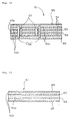
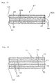
- Fig. 11 shows in cross section a printed board 61 according to a second embodiment of the present invention.
- the printed board 61 has a power supply layer 63 disposed on an upper surface of a first insulating layer 62a and a ground layer 64 disposed on a lower surface of the first insulating layer 62a.
- Second insulating layers 62b are disposed respectively on outer surfaces of the power supply layer 63 and the ground layer 64.
- Signal layers 65 are disposed respectively on outer surfaces of the second insulating layers 62b.
- Toroidal spiral coil inductors (not shown) are disposed between the power supply layer 63 and the ground layer 64.
- Conductor lines and through holes (not shown) of the toroidal spiral coil inductors, the power supply layer 63, the ground layer 64, device power terminals (not shown), device ground terminals (not shown), circuit devices (not shown) which are to be connected to the printed board 61, and decoupling capacitors (not shown) are identical to those of the printed board shown in Figs. 2 through 5, and will not be described in detail below.
- the first insulating layer 62a is made of an epoxy-base insulating solvent mixed with a magnetic material.
- the magnetic material may comprise, for example, fine powder of Ni - Zn ferrite, fine powder of Mn - Zn ferrite, fine powder of Li ferrite, fine powder of Sendust, a fine powder of amorphous material, and a fine powder of Permalloy.
- Fig. 12 shows a modified printed board 61' having a first insulating layer 62a which comprises an amorphous magnetic foil 67 with their opposite surfaces each coated with an insulating coating 66.
- Other details of the modified printed board 61' are identical to those of the printed board 61 shown in Fig. 11.
- the first insulating layer 62a mixed with a magnetic material functions as the magnetic core of the toroidal spiral coil inductors disposed between the power supply layer 63 and the ground layer 64. Therefore, the inductance of the toroidal spiral coil inductors increases.
- the first insulating layer 62a can be formed simply by mixing a magnetic material with an epoxy-base insulating solvent. Therefore, the process of fabricating the printed board is not greatly affected by employing the first insulating layer 62a. If the amorphous magnetic foil 67 with the insulating coating 66 on its opposite surfaces is employed, then since no time is required for an epoxy-base insulating solvent to solidify, the time required to form the amorphous magnetic foil 67 is relatively short.
- the printed boards 61, 61' have four layers including the power supply layer 63, the ground layer 64, and the two signal layers 65 in addition to the insulating layers.
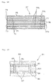
- a printed board 71 according to a third embodiment of the present invention and a modified printed board 71' have six layers including power supply layers 73, ground layers 74, and signal layers 75 in addition to first, second, and third insulating layers 72a, 72b, 72c.
- the printed boards 71, 71', the second insulating layers 72b, the third insulating layers 72c, the power supply layers 73, the ground layers 74, the signal layers 75, and the toroidal spiral coil inductors (not shown) disposed between the power supply layers 73 are identical to the corresponding members of the printed board 41 shown in Fig. 9, and will not be described in detail below.
- the first insulating layer 72a is mixed with an insulating magnetic materiel, as with the printed board 61 shown in Fig. 11.
- the printed board 71' shown in Fig. 14 has a first insulating layer which comprises an amorphous magnetic foil 77 with their opposite surfaces each coated with an insulating coating 76, as with the printed board 61' shown in Fig. 12.
- Fig. 15 shows in fragmentary cross section a toroidal spiral coil inductor in a printed board which is a modification of the printed boards shown in Figs. 11 through 14.
- the first insulating layer contains a magnetic material in its entirety. However, the magnetic material may not be present in the whole region of the first insulating layer.
- a magnetic material is present only in a coil interior 88 of a toroidal spiral coil inductor which is disposed in a region of a first insulating layer 82a that is surrounded by conductor lines 85, 87 in a power supply layer 83 and a ground layer 84, and through holes 86 interconnecting the conductor lines 85, 87, i.e., formed between the power supply layer 83 and the ground layer 84. Therefore, the first insulating layer 82a in the coil interior 88 functions as the magnetic core of the toroidal spiral coil inductor, increasing the inductance of the toroidal spiral coil inductor.
Landscapes
- Engineering & Computer Science (AREA)
- Microelectronics & Electronic Packaging (AREA)
- Physics & Mathematics (AREA)
- Electromagnetism (AREA)
- Structure Of Printed Boards (AREA)
- Filters And Equalizers (AREA)
- Coils Or Transformers For Communication (AREA)
- Parts Printed On Printed Circuit Boards (AREA)
Applications Claiming Priority (3)
| Application Number | Priority Date | Filing Date | Title |
|---|---|---|---|
| JP9128761A JP3058121B2 (ja) | 1997-05-19 | 1997-05-19 | プリント基板 |
| JP12876197 | 1997-05-19 | ||
| JP128761/97 | 1997-05-19 |
Publications (2)
| Publication Number | Publication Date |
|---|---|
| EP0880309A2 true EP0880309A2 (fr) | 1998-11-25 |
| EP0880309A3 EP0880309A3 (fr) | 2001-08-01 |
Family
ID=14992822
Family Applications (1)
| Application Number | Title | Priority Date | Filing Date |
|---|---|---|---|
| EP98108818A Withdrawn EP0880309A3 (fr) | 1997-05-19 | 1998-05-14 | Réduction du bruit électromagnétique émis par un panneau à circuit imprimé |
Country Status (8)
| Country | Link |
|---|---|
| US (1) | US6002593A (fr) |
| EP (1) | EP0880309A3 (fr) |
| JP (1) | JP3058121B2 (fr) |
| KR (1) | KR100294956B1 (fr) |
| CN (1) | CN1108733C (fr) |
| AU (1) | AU728934B2 (fr) |
| CA (1) | CA2237923C (fr) |
| TW (1) | TW388189B (fr) |
Cited By (3)
| Publication number | Priority date | Publication date | Assignee | Title |
|---|---|---|---|---|
| DE10121479C1 (de) * | 2001-05-03 | 2002-11-07 | Bosch Gmbh Robert | Zwischen verschiedenen Leuchtfunktionen umschaltbarer Kraftfahrzeugscheinwerfer mit einer Filterschaltung zur Reduzierung einer Störabstrahlung einer Endstufe |
| EP1955343A4 (fr) * | 2005-11-30 | 2009-07-22 | Avocent Corp | Ligne a retard a solenoide multicouche sur circuit imprime |
| WO2020123068A1 (fr) * | 2018-12-13 | 2020-06-18 | Qualcomm Incorporated | Substrat comprenant au moins un plan de masse à motifs pour blindage |
Families Citing this family (47)
| Publication number | Priority date | Publication date | Assignee | Title |
|---|---|---|---|---|
| JP3036629B2 (ja) * | 1996-10-07 | 2000-04-24 | 富士ゼロックス株式会社 | プリント配線基板装置 |
| JP2877132B2 (ja) * | 1997-03-26 | 1999-03-31 | 日本電気株式会社 | 多層プリント基板とその製造方法 |
| JP3214472B2 (ja) * | 1998-12-04 | 2001-10-02 | 日本電気株式会社 | 多層プリント回路基板 |
| JP3267274B2 (ja) | 1999-08-13 | 2002-03-18 | 日本電気株式会社 | 多層プリント基板 |
| JP3232562B2 (ja) | 1999-10-22 | 2001-11-26 | 日本電気株式会社 | 電磁干渉抑制部品および電磁干渉抑制回路 |
| JP2001223449A (ja) * | 2000-02-09 | 2001-08-17 | Toshiba Corp | 多層プリント基板 |
| JP2001332825A (ja) * | 2000-03-14 | 2001-11-30 | Fuji Xerox Co Ltd | 回路基板装置及び設計支援装置 |
| KR100336455B1 (ko) * | 2000-03-29 | 2002-05-11 | 문규 | 이중층 파워라인 구조를 갖는 뮤추얼 인덕터를 이용한파워라인 동시 동작 노이즈 최소화장치 |
| JP2002164713A (ja) * | 2000-11-28 | 2002-06-07 | Tdk Corp | 被覆シート、該シートを用いたトリプレート線路、該シートを用いたコンピュータ用信号バス及び該シートを用いた電子回路被覆構造 |
| JP3586435B2 (ja) * | 2001-03-30 | 2004-11-10 | ユーディナデバイス株式会社 | 高周波半導体装置 |
| JP3818864B2 (ja) * | 2001-03-30 | 2006-09-06 | ユーディナデバイス株式会社 | 高周波半導体装置 |
| US6489853B1 (en) | 2002-03-19 | 2002-12-03 | Z-Communications, Inc. | Low phase noise oscillator |
| US7259639B2 (en) * | 2002-03-29 | 2007-08-21 | M/A-Com Eurotec, B.V. | Inductor topologies and decoupling structures for filters used in broadband applications, and design methodology thereof |
| KR100957257B1 (ko) * | 2002-04-08 | 2010-05-12 | 소니 주식회사 | 신호 수신 장치 및 신호 수신 회로 |
| US6806793B2 (en) * | 2002-12-13 | 2004-10-19 | International Business Machines Corporation | MLC frequency selective circuit structures |
| CN1322386C (zh) * | 2004-01-09 | 2007-06-20 | 佛山市顺德区顺达电脑厂有限公司 | 可抑制电磁干扰的抵销电路及其运行方法 |
| US7382629B2 (en) * | 2004-05-11 | 2008-06-03 | Via Technologies, Inc. | Circuit substrate and method of manufacturing plated through slot thereon |
| US7323787B2 (en) * | 2005-01-25 | 2008-01-29 | Alcatel | Off-grid decoupling of ball grid array (BGA) devices and method |
| KR100801288B1 (ko) | 2006-02-28 | 2008-02-11 | 인천대학교 산학협력단 | 평면 회로 기판〔pcb〕전력 공급 장치 |
| US7875955B1 (en) | 2006-03-09 | 2011-01-25 | National Semiconductor Corporation | On-chip power inductor |
| KR100733279B1 (ko) * | 2006-03-14 | 2007-06-28 | 대덕전자 주식회사 | 인덕터 내장형 인쇄 회로 기판 제조 방법 |
| JP4659666B2 (ja) * | 2006-04-18 | 2011-03-30 | 株式会社日立製作所 | 放送受信装置、及び、そのチューナ装置とそのための分配器 |
| JP2008124105A (ja) * | 2006-11-09 | 2008-05-29 | Seiko Epson Corp | 多層プリント配線板 |
| CN101188902B (zh) * | 2006-11-17 | 2011-08-24 | 鸿富锦精密工业(深圳)有限公司 | 印刷电路板 |
| JP5354949B2 (ja) * | 2007-06-19 | 2013-11-27 | キヤノン株式会社 | プリント回路板 |
| US8310840B2 (en) | 2007-08-07 | 2012-11-13 | Samsung Electro-Mechanics Co., Ltd. | Electromagnetic bandgap structure and printed circuit board |
| US8169790B2 (en) | 2007-08-07 | 2012-05-01 | Samsung Electro-Mechanics Co., Ltd. | Electromagnetic bandgap structure and printed circuit board |
| KR100998718B1 (ko) * | 2008-01-21 | 2010-12-07 | 삼성전기주식회사 | 전자기 밴드갭 구조물 및 인쇄회로기판 |
| US8077000B2 (en) * | 2008-01-21 | 2011-12-13 | Samsung Electro-Mechanics Co., Ltd. | Electromagnetic bandgap structure and printed circuit board |
| US7956493B2 (en) | 2008-08-11 | 2011-06-07 | Infineon Technologies Ag | Integrated circuit and method for manufacturing an integrated circuit |
| KR101055457B1 (ko) * | 2009-04-07 | 2011-08-08 | 포항공과대학교 산학협력단 | 전자기 밴드갭 구조물 및 이를 포함하는 인쇄회로기판 |
| KR101055483B1 (ko) * | 2009-04-07 | 2011-08-08 | 포항공과대학교 산학협력단 | 전자기 밴드갭 구조물 및 이를 포함하는 인쇄회로기판 |
| KR101072591B1 (ko) * | 2009-08-10 | 2011-10-11 | 삼성전기주식회사 | Emi 노이즈 저감 인쇄회로기판 |
| KR101021548B1 (ko) * | 2009-09-18 | 2011-03-16 | 삼성전기주식회사 | 전자기 밴드갭 구조를 구비하는 인쇄회로기판 |
| KR101021551B1 (ko) * | 2009-09-22 | 2011-03-16 | 삼성전기주식회사 | 전자기 밴드갭 구조를 구비하는 인쇄회로기판 |
| KR101023541B1 (ko) * | 2009-09-22 | 2011-03-21 | 삼성전기주식회사 | Emi 노이즈 저감 인쇄회로기판 |
| KR20110134200A (ko) * | 2010-06-08 | 2011-12-14 | 삼성전기주식회사 | 전자기 밴드갭 구조물을 포함하는 emi 노이즈 차폐 기판 |
| US8631706B2 (en) | 2010-07-21 | 2014-01-21 | International Business Machines Corporation | Noise suppressor for semiconductor packages |
| CN102387657A (zh) * | 2010-08-31 | 2012-03-21 | 鸿富锦精密工业(深圳)有限公司 | 电路板 |
| JP5833465B2 (ja) * | 2011-07-25 | 2015-12-16 | 株式会社日本自動車部品総合研究所 | 電流検出器 |
| US20140369010A1 (en) * | 2012-01-27 | 2014-12-18 | Panasonic Corporation | Image display apparatus provided with back cover |
| JP5893484B2 (ja) * | 2012-04-09 | 2016-03-23 | キヤノン株式会社 | プリント回路板及びプリント配線板 |
| CN205071428U (zh) * | 2015-07-20 | 2016-03-02 | 西安中兴新软件有限责任公司 | 一种电磁带隙结构及印刷电路板 |
| JP2018073878A (ja) * | 2016-10-25 | 2018-05-10 | 矢崎総業株式会社 | 基板、及び、ノイズフィルタ構造 |
| EP3346478B1 (fr) * | 2017-01-09 | 2019-05-01 | Siemens Aktiengesellschaft | Système de condensateur et système sous-marin le comprenant |
| CN111309197B (zh) * | 2020-01-19 | 2024-08-16 | 深圳市鸿合创新信息技术有限责任公司 | 感应膜及其制作方法、感应板及其制作方法和显示设备 |
| CN115633111B (zh) * | 2022-12-21 | 2023-05-16 | 荣耀终端有限公司 | 线路板、相关装置和控制方法 |
Family Cites Families (20)
| Publication number | Priority date | Publication date | Assignee | Title |
|---|---|---|---|---|
| JPS5880805A (ja) * | 1981-11-09 | 1983-05-16 | Hitachi Ltd | インダクタンスコイルをそなえた配線板 |
| JPS58157112A (ja) * | 1982-03-15 | 1983-09-19 | Matsushita Electric Works Ltd | プリントインダクタンス |
| JPS58157109A (ja) * | 1982-03-15 | 1983-09-19 | Matsushita Electric Works Ltd | プリントインダクタンス |
| JPS58188115A (ja) * | 1982-04-27 | 1983-11-02 | Sanyo Electric Co Ltd | 誘導性素子の形成方法 |
| JPS60196910A (ja) * | 1984-03-19 | 1985-10-05 | Fujitsu Ltd | ハイブリツドic及びその製造方法 |
| JPS62139395A (ja) * | 1985-12-13 | 1987-06-23 | 松下電器産業株式会社 | 多機能回路基板 |
| JPS63300593A (ja) * | 1987-05-29 | 1988-12-07 | Nec Corp | セラミック複合基板 |
| JPS6425497A (en) * | 1987-07-21 | 1989-01-27 | Matsushita Electric Industrial Co Ltd | Inductance element |
| JPH02181961A (ja) * | 1989-01-09 | 1990-07-16 | Nec Corp | 集積回路装置 |
| JPH03214863A (ja) * | 1990-01-19 | 1991-09-20 | Toshiba Corp | ファクシミリ装置 |
| JP2741090B2 (ja) * | 1990-03-23 | 1998-04-15 | キヤノン株式会社 | プリント基板 |
| US4984146A (en) * | 1990-03-27 | 1991-01-08 | International Business Machines Corporation | Suppression of radiated EMI for power supplies |
| DE4027994A1 (de) * | 1990-09-04 | 1992-03-05 | Gw Elektronik Gmbh | Hf-magnetspulenanordnung und verfahren zu ihrer herstellung |
| JP2829151B2 (ja) * | 1991-03-04 | 1998-11-25 | メルコアジャパン株式会社 | 導電材接合素子及び回路構成 |
| JPH06112655A (ja) * | 1992-09-29 | 1994-04-22 | Matsushita Electric Ind Co Ltd | コイル内蔵多層印刷配線板およびその製造方法 |
| DE4306416A1 (de) * | 1993-03-02 | 1994-09-08 | Kolbe & Co Hans | Spulenstruktur für eine Leiterplattenanordnung |
| JPH0845738A (ja) * | 1994-07-27 | 1996-02-16 | Canon Inc | インダクタンス素子 |
| JPH08293416A (ja) * | 1995-04-24 | 1996-11-05 | Canon Inc | ノイズフィルタ |
| US5781091A (en) * | 1995-07-24 | 1998-07-14 | Autosplice Systems Inc. | Electronic inductive device and method for manufacturing |
| JPH11140915A (ja) * | 1997-11-07 | 1999-05-25 | Hitachi Constr Mach Co Ltd | 建設機械の油圧回路 |
-
1997
- 1997-05-19 JP JP9128761A patent/JP3058121B2/ja not_active Expired - Fee Related
-
1998
- 1998-05-14 EP EP98108818A patent/EP0880309A3/fr not_active Withdrawn
- 1998-05-15 CA CA002237923A patent/CA2237923C/fr not_active Expired - Fee Related
- 1998-05-15 TW TW087107587A patent/TW388189B/zh not_active IP Right Cessation
- 1998-05-18 KR KR1019980017796A patent/KR100294956B1/ko not_active Expired - Fee Related
- 1998-05-18 AU AU67063/98A patent/AU728934B2/en not_active Ceased
- 1998-05-19 CN CN98102153A patent/CN1108733C/zh not_active Expired - Fee Related
- 1998-05-19 US US09/081,137 patent/US6002593A/en not_active Expired - Fee Related
Cited By (6)
| Publication number | Priority date | Publication date | Assignee | Title |
|---|---|---|---|---|
| DE10121479C1 (de) * | 2001-05-03 | 2002-11-07 | Bosch Gmbh Robert | Zwischen verschiedenen Leuchtfunktionen umschaltbarer Kraftfahrzeugscheinwerfer mit einer Filterschaltung zur Reduzierung einer Störabstrahlung einer Endstufe |
| EP1955343A4 (fr) * | 2005-11-30 | 2009-07-22 | Avocent Corp | Ligne a retard a solenoide multicouche sur circuit imprime |
| US8031033B2 (en) | 2005-11-30 | 2011-10-04 | Avocent Corporation | Printed multilayer solenoid delay line having at least two sub-sets with different patterns |
| WO2020123068A1 (fr) * | 2018-12-13 | 2020-06-18 | Qualcomm Incorporated | Substrat comprenant au moins un plan de masse à motifs pour blindage |
| CN113366923A (zh) * | 2018-12-13 | 2021-09-07 | 高通股份有限公司 | 包括用于屏蔽的至少一个图案化接地平面的基板 |
| US11270951B2 (en) | 2018-12-13 | 2022-03-08 | Qualcomm Incorporated | Substrate comprising at least one patterned ground plane for shielding |
Also Published As
| Publication number | Publication date |
|---|---|
| CN1108733C (zh) | 2003-05-14 |
| AU728934B2 (en) | 2001-01-18 |
| JPH10321973A (ja) | 1998-12-04 |
| CA2237923A1 (fr) | 1998-11-19 |
| CN1201363A (zh) | 1998-12-09 |
| EP0880309A3 (fr) | 2001-08-01 |
| CA2237923C (fr) | 2001-04-17 |
| KR19980087147A (ko) | 1998-12-05 |
| KR100294956B1 (ko) | 2001-07-12 |
| US6002593A (en) | 1999-12-14 |
| JP3058121B2 (ja) | 2000-07-04 |
| AU6706398A (en) | 1998-11-19 |
| TW388189B (en) | 2000-04-21 |
Similar Documents
| Publication | Publication Date | Title |
|---|---|---|
| US6002593A (en) | Reducing electromagnetic noise radiated from a printed board | |
| EP0880150B1 (fr) | Plaque à circuit imprimé | |
| US6903938B2 (en) | Printed circuit board | |
| US6111479A (en) | Laminate printed circuit board with a magnetic layer | |
| KR100382804B1 (ko) | 다층 프린트 기판 | |
| CN1333492C (zh) | 减小环形天线寄生效应的技术 | |
| CN110603736B (zh) | 大面积可扩展的高度共振无线电力线圈 | |
| JP2734447B2 (ja) | 多層プリント基板 | |
| JP4916807B2 (ja) | 電圧検出用プリント基板及びそれを用いた電圧検出器 | |
| US6297965B1 (en) | Wiring arrangement including capacitors for suppressing electromagnetic wave radiation from a printed circuit board | |
| US7342477B2 (en) | Inductor | |
| EP0393644B1 (fr) | Filtre antiparasites LC | |
| WO1998005048A1 (fr) | Transformateur/inducteur plan a faible rayonnement et procede correspondant | |
| HK1008407B (en) | Lc noise filter | |
| US7538653B2 (en) | Grounding of magnetic cores | |
| JP2988421B2 (ja) | Emi抑制多層プリント基板 | |
| EP4002402B1 (fr) | Transformateur planaire fendu symétrique | |
| CN113345700A (zh) | 线圈部件以及具备其的电路基板 | |
| JPS62139395A (ja) | 多機能回路基板 | |
| CN114284237B (zh) | 具有电源管理功能的金属布线层结构及其制备方法 | |
| JPH06132131A (ja) | 薄膜形磁気誘導素子 | |
| Wolf | Integral Passive Components | |
| JPH02215213A (ja) | Lcノイズフィルタおよびこれを用いたpcボード |
Legal Events
| Date | Code | Title | Description |
|---|---|---|---|
| PUAI | Public reference made under article 153(3) epc to a published international application that has entered the european phase |
Free format text: ORIGINAL CODE: 0009012 |
|
| AK | Designated contracting states |
Kind code of ref document: A2 Designated state(s): DE FR GB |
|
| AX | Request for extension of the european patent |
Free format text: AL;LT;LV;MK;RO;SI |
|
| PUAL | Search report despatched |
Free format text: ORIGINAL CODE: 0009013 |
|
| AK | Designated contracting states |
Kind code of ref document: A3 Designated state(s): AT BE CH CY DE DK ES FI FR GB GR IE IT LI LU MC NL PT SE |
|
| AX | Request for extension of the european patent |
Free format text: AL;LT;LV;MK;RO;SI |
|
| 17P | Request for examination filed |
Effective date: 20011022 |
|
| AKX | Designation fees paid |
Free format text: DE FR GB |
|
| GRAP | Despatch of communication of intention to grant a patent |
Free format text: ORIGINAL CODE: EPIDOSNIGR1 |
|
| STAA | Information on the status of an ep patent application or granted ep patent |
Free format text: STATUS: THE APPLICATION HAS BEEN WITHDRAWN |
|
| 18W | Application withdrawn |
Effective date: 20041207 |