EP0881671A2 - Méthode de fabrication d'un dispositif semiconducteur - Google Patents
Méthode de fabrication d'un dispositif semiconducteur Download PDFInfo
- Publication number
- EP0881671A2 EP0881671A2 EP98109536A EP98109536A EP0881671A2 EP 0881671 A2 EP0881671 A2 EP 0881671A2 EP 98109536 A EP98109536 A EP 98109536A EP 98109536 A EP98109536 A EP 98109536A EP 0881671 A2 EP0881671 A2 EP 0881671A2
- Authority
- EP
- European Patent Office
- Prior art keywords
- submount
- emitting laser
- surface emitting
- semiconductor device
- fabricating
- Prior art date
- Legal status (The legal status is an assumption and is not a legal conclusion. Google has not performed a legal analysis and makes no representation as to the accuracy of the status listed.)
- Withdrawn
Links
Images





Classifications
-
- H—ELECTRICITY
- H10—SEMICONDUCTOR DEVICES; ELECTRIC SOLID-STATE DEVICES NOT OTHERWISE PROVIDED FOR
- H10P—GENERIC PROCESSES OR APPARATUS FOR THE MANUFACTURE OR TREATMENT OF DEVICES COVERED BY CLASS H10
- H10P72/00—Handling or holding of wafers, substrates or devices during manufacture or treatment thereof
- H10P72/70—Handling or holding of wafers, substrates or devices during manufacture or treatment thereof for supporting or gripping
- H10P72/74—Handling or holding of wafers, substrates or devices during manufacture or treatment thereof for supporting or gripping using temporarily an auxiliary support
-
- H—ELECTRICITY
- H01—ELECTRIC ELEMENTS
- H01S—DEVICES USING THE PROCESS OF LIGHT AMPLIFICATION BY STIMULATED EMISSION OF RADIATION [LASER] TO AMPLIFY OR GENERATE LIGHT; DEVICES USING STIMULATED EMISSION OF ELECTROMAGNETIC RADIATION IN WAVE RANGES OTHER THAN OPTICAL
- H01S5/00—Semiconductor lasers
- H01S5/02—Structural details or components not essential to laser action
- H01S5/022—Mountings; Housings
- H01S5/0235—Method for mounting laser chips
- H01S5/02355—Fixing laser chips on mounts
- H01S5/0237—Fixing laser chips on mounts by soldering
-
- H—ELECTRICITY
- H01—ELECTRIC ELEMENTS
- H01S—DEVICES USING THE PROCESS OF LIGHT AMPLIFICATION BY STIMULATED EMISSION OF RADIATION [LASER] TO AMPLIFY OR GENERATE LIGHT; DEVICES USING STIMULATED EMISSION OF ELECTROMAGNETIC RADIATION IN WAVE RANGES OTHER THAN OPTICAL
- H01S5/00—Semiconductor lasers
- H01S5/02—Structural details or components not essential to laser action
- H01S5/026—Monolithically integrated components, e.g. waveguides, monitoring photo-detectors, drivers
- H01S5/0261—Non-optical elements, e.g. laser driver components, heaters
-
- H—ELECTRICITY
- H01—ELECTRIC ELEMENTS
- H01S—DEVICES USING THE PROCESS OF LIGHT AMPLIFICATION BY STIMULATED EMISSION OF RADIATION [LASER] TO AMPLIFY OR GENERATE LIGHT; DEVICES USING STIMULATED EMISSION OF ELECTROMAGNETIC RADIATION IN WAVE RANGES OTHER THAN OPTICAL
- H01S5/00—Semiconductor lasers
- H01S5/04—Processes or apparatus for excitation, e.g. pumping, e.g. by electron beams
- H01S5/042—Electrical excitation ; Circuits therefor
- H01S5/0425—Electrodes, e.g. characterised by the structure
- H01S5/04256—Electrodes, e.g. characterised by the structure characterised by the configuration
- H01S5/04257—Electrodes, e.g. characterised by the structure characterised by the configuration having positive and negative electrodes on the same side of the substrate
-
- H—ELECTRICITY
- H10—SEMICONDUCTOR DEVICES; ELECTRIC SOLID-STATE DEVICES NOT OTHERWISE PROVIDED FOR
- H10W—GENERIC PACKAGES, INTERCONNECTIONS, CONNECTORS OR OTHER CONSTRUCTIONAL DETAILS OF DEVICES COVERED BY CLASS H10
- H10W74/00—Encapsulations, e.g. protective coatings
- H10W74/01—Manufacture or treatment
- H10W74/012—Manufacture or treatment of encapsulations on active surfaces of flip-chip devices, e.g. forming underfills
-
- H—ELECTRICITY
- H10—SEMICONDUCTOR DEVICES; ELECTRIC SOLID-STATE DEVICES NOT OTHERWISE PROVIDED FOR
- H10W—GENERIC PACKAGES, INTERCONNECTIONS, CONNECTORS OR OTHER CONSTRUCTIONAL DETAILS OF DEVICES COVERED BY CLASS H10
- H10W74/00—Encapsulations, e.g. protective coatings
- H10W74/10—Encapsulations, e.g. protective coatings characterised by their shape or disposition
- H10W74/15—Encapsulations, e.g. protective coatings characterised by their shape or disposition on active surfaces of flip-chip devices, e.g. underfills
-
- H—ELECTRICITY
- H10—SEMICONDUCTOR DEVICES; ELECTRIC SOLID-STATE DEVICES NOT OTHERWISE PROVIDED FOR
- H10W—GENERIC PACKAGES, INTERCONNECTIONS, CONNECTORS OR OTHER CONSTRUCTIONAL DETAILS OF DEVICES COVERED BY CLASS H10
- H10W90/00—Package configurations
- H10W90/20—Configurations of stacked chips
- H10W90/293—Configurations of stacked chips characterised by non-galvanic coupling between the chips, e.g. capacitive coupling
-
- H—ELECTRICITY
- H01—ELECTRIC ELEMENTS
- H01S—DEVICES USING THE PROCESS OF LIGHT AMPLIFICATION BY STIMULATED EMISSION OF RADIATION [LASER] TO AMPLIFY OR GENERATE LIGHT; DEVICES USING STIMULATED EMISSION OF ELECTROMAGNETIC RADIATION IN WAVE RANGES OTHER THAN OPTICAL
- H01S2301/00—Functional characteristics
- H01S2301/17—Semiconductor lasers comprising special layers
- H01S2301/176—Specific passivation layers on surfaces other than the emission facet
-
- H—ELECTRICITY
- H01—ELECTRIC ELEMENTS
- H01S—DEVICES USING THE PROCESS OF LIGHT AMPLIFICATION BY STIMULATED EMISSION OF RADIATION [LASER] TO AMPLIFY OR GENERATE LIGHT; DEVICES USING STIMULATED EMISSION OF ELECTROMAGNETIC RADIATION IN WAVE RANGES OTHER THAN OPTICAL
- H01S5/00—Semiconductor lasers
- H01S5/02—Structural details or components not essential to laser action
- H01S5/0206—Substrates, e.g. growth, shape, material, removal or bonding
- H01S5/0207—Substrates having a special shape
-
- H—ELECTRICITY
- H01—ELECTRIC ELEMENTS
- H01S—DEVICES USING THE PROCESS OF LIGHT AMPLIFICATION BY STIMULATED EMISSION OF RADIATION [LASER] TO AMPLIFY OR GENERATE LIGHT; DEVICES USING STIMULATED EMISSION OF ELECTROMAGNETIC RADIATION IN WAVE RANGES OTHER THAN OPTICAL
- H01S5/00—Semiconductor lasers
- H01S5/02—Structural details or components not essential to laser action
- H01S5/0206—Substrates, e.g. growth, shape, material, removal or bonding
- H01S5/0217—Removal of the substrate
-
- H—ELECTRICITY
- H01—ELECTRIC ELEMENTS
- H01S—DEVICES USING THE PROCESS OF LIGHT AMPLIFICATION BY STIMULATED EMISSION OF RADIATION [LASER] TO AMPLIFY OR GENERATE LIGHT; DEVICES USING STIMULATED EMISSION OF ELECTROMAGNETIC RADIATION IN WAVE RANGES OTHER THAN OPTICAL
- H01S5/00—Semiconductor lasers
- H01S5/02—Structural details or components not essential to laser action
- H01S5/022—Mountings; Housings
- H01S5/023—Mount members, e.g. sub-mount members
- H01S5/02325—Mechanically integrated components on mount members or optical micro-benches
-
- H—ELECTRICITY
- H01—ELECTRIC ELEMENTS
- H01S—DEVICES USING THE PROCESS OF LIGHT AMPLIFICATION BY STIMULATED EMISSION OF RADIATION [LASER] TO AMPLIFY OR GENERATE LIGHT; DEVICES USING STIMULATED EMISSION OF ELECTROMAGNETIC RADIATION IN WAVE RANGES OTHER THAN OPTICAL
- H01S5/00—Semiconductor lasers
- H01S5/02—Structural details or components not essential to laser action
- H01S5/022—Mountings; Housings
- H01S5/0233—Mounting configuration of laser chips
- H01S5/0234—Up-side down mountings, e.g. Flip-chip, epi-side down mountings or junction down mountings
-
- H—ELECTRICITY
- H01—ELECTRIC ELEMENTS
- H01S—DEVICES USING THE PROCESS OF LIGHT AMPLIFICATION BY STIMULATED EMISSION OF RADIATION [LASER] TO AMPLIFY OR GENERATE LIGHT; DEVICES USING STIMULATED EMISSION OF ELECTROMAGNETIC RADIATION IN WAVE RANGES OTHER THAN OPTICAL
- H01S5/00—Semiconductor lasers
- H01S5/02—Structural details or components not essential to laser action
- H01S5/026—Monolithically integrated components, e.g. waveguides, monitoring photo-detectors, drivers
-
- H—ELECTRICITY
- H01—ELECTRIC ELEMENTS
- H01S—DEVICES USING THE PROCESS OF LIGHT AMPLIFICATION BY STIMULATED EMISSION OF RADIATION [LASER] TO AMPLIFY OR GENERATE LIGHT; DEVICES USING STIMULATED EMISSION OF ELECTROMAGNETIC RADIATION IN WAVE RANGES OTHER THAN OPTICAL
- H01S5/00—Semiconductor lasers
- H01S5/02—Structural details or components not essential to laser action
- H01S5/028—Coatings ; Treatment of the laser facets, e.g. etching, passivation layers or reflecting layers
-
- H—ELECTRICITY
- H01—ELECTRIC ELEMENTS
- H01S—DEVICES USING THE PROCESS OF LIGHT AMPLIFICATION BY STIMULATED EMISSION OF RADIATION [LASER] TO AMPLIFY OR GENERATE LIGHT; DEVICES USING STIMULATED EMISSION OF ELECTROMAGNETIC RADIATION IN WAVE RANGES OTHER THAN OPTICAL
- H01S5/00—Semiconductor lasers
- H01S5/06—Arrangements for controlling the laser output parameters, e.g. by operating on the active medium
- H01S5/068—Stabilisation of laser output parameters
- H01S5/0683—Stabilisation of laser output parameters by monitoring the optical output parameters
-
- H—ELECTRICITY
- H01—ELECTRIC ELEMENTS
- H01S—DEVICES USING THE PROCESS OF LIGHT AMPLIFICATION BY STIMULATED EMISSION OF RADIATION [LASER] TO AMPLIFY OR GENERATE LIGHT; DEVICES USING STIMULATED EMISSION OF ELECTROMAGNETIC RADIATION IN WAVE RANGES OTHER THAN OPTICAL
- H01S5/00—Semiconductor lasers
- H01S5/10—Construction or shape of the optical resonator, e.g. extended or external cavity, coupled cavities, bent-guide, varying width, thickness or composition of the active region
- H01S5/18—Surface-emitting [SE] lasers, e.g. having both horizontal and vertical cavities
- H01S5/183—Surface-emitting [SE] lasers, e.g. having both horizontal and vertical cavities having only vertical cavities, e.g. vertical cavity surface-emitting lasers [VCSEL]
- H01S5/18305—Surface-emitting [SE] lasers, e.g. having both horizontal and vertical cavities having only vertical cavities, e.g. vertical cavity surface-emitting lasers [VCSEL] with emission through the substrate, i.e. bottom emission
-
- H—ELECTRICITY
- H01—ELECTRIC ELEMENTS
- H01S—DEVICES USING THE PROCESS OF LIGHT AMPLIFICATION BY STIMULATED EMISSION OF RADIATION [LASER] TO AMPLIFY OR GENERATE LIGHT; DEVICES USING STIMULATED EMISSION OF ELECTROMAGNETIC RADIATION IN WAVE RANGES OTHER THAN OPTICAL
- H01S5/00—Semiconductor lasers
- H01S5/10—Construction or shape of the optical resonator, e.g. extended or external cavity, coupled cavities, bent-guide, varying width, thickness or composition of the active region
- H01S5/18—Surface-emitting [SE] lasers, e.g. having both horizontal and vertical cavities
- H01S5/183—Surface-emitting [SE] lasers, e.g. having both horizontal and vertical cavities having only vertical cavities, e.g. vertical cavity surface-emitting lasers [VCSEL]
- H01S5/18361—Structure of the reflectors, e.g. hybrid mirrors
- H01S5/1838—Reflector bonded by wafer fusion or by an intermediate compound
-
- H—ELECTRICITY
- H01—ELECTRIC ELEMENTS
- H01S—DEVICES USING THE PROCESS OF LIGHT AMPLIFICATION BY STIMULATED EMISSION OF RADIATION [LASER] TO AMPLIFY OR GENERATE LIGHT; DEVICES USING STIMULATED EMISSION OF ELECTROMAGNETIC RADIATION IN WAVE RANGES OTHER THAN OPTICAL
- H01S5/00—Semiconductor lasers
- H01S5/10—Construction or shape of the optical resonator, e.g. extended or external cavity, coupled cavities, bent-guide, varying width, thickness or composition of the active region
- H01S5/18—Surface-emitting [SE] lasers, e.g. having both horizontal and vertical cavities
- H01S5/183—Surface-emitting [SE] lasers, e.g. having both horizontal and vertical cavities having only vertical cavities, e.g. vertical cavity surface-emitting lasers [VCSEL]
- H01S5/18386—Details of the emission surface for influencing the near- or far-field, e.g. a grating on the surface
- H01S5/18388—Lenses
-
- H—ELECTRICITY
- H01—ELECTRIC ELEMENTS
- H01S—DEVICES USING THE PROCESS OF LIGHT AMPLIFICATION BY STIMULATED EMISSION OF RADIATION [LASER] TO AMPLIFY OR GENERATE LIGHT; DEVICES USING STIMULATED EMISSION OF ELECTROMAGNETIC RADIATION IN WAVE RANGES OTHER THAN OPTICAL
- H01S5/00—Semiconductor lasers
- H01S5/40—Arrangement of two or more semiconductor lasers, not provided for in groups H01S5/02 - H01S5/30
- H01S5/42—Arrays of surface emitting lasers
- H01S5/423—Arrays of surface emitting lasers having a vertical cavity
-
- H—ELECTRICITY
- H10—SEMICONDUCTOR DEVICES; ELECTRIC SOLID-STATE DEVICES NOT OTHERWISE PROVIDED FOR
- H10P—GENERIC PROCESSES OR APPARATUS FOR THE MANUFACTURE OR TREATMENT OF DEVICES COVERED BY CLASS H10
- H10P72/00—Handling or holding of wafers, substrates or devices during manufacture or treatment thereof
- H10P72/70—Handling or holding of wafers, substrates or devices during manufacture or treatment thereof for supporting or gripping
- H10P72/74—Handling or holding of wafers, substrates or devices during manufacture or treatment thereof for supporting or gripping using temporarily an auxiliary support
- H10P72/743—Handling or holding of wafers, substrates or devices during manufacture or treatment thereof for supporting or gripping using temporarily an auxiliary support used as a support during manufacture of interconnect decals or build up layers
-
- H—ELECTRICITY
- H10—SEMICONDUCTOR DEVICES; ELECTRIC SOLID-STATE DEVICES NOT OTHERWISE PROVIDED FOR
- H10W—GENERIC PACKAGES, INTERCONNECTIONS, CONNECTORS OR OTHER CONSTRUCTIONAL DETAILS OF DEVICES COVERED BY CLASS H10
- H10W72/00—Interconnections or connectors in packages
- H10W72/071—Connecting or disconnecting
- H10W72/072—Connecting or disconnecting of bump connectors
-
- H—ELECTRICITY
- H10—SEMICONDUCTOR DEVICES; ELECTRIC SOLID-STATE DEVICES NOT OTHERWISE PROVIDED FOR
- H10W—GENERIC PACKAGES, INTERCONNECTIONS, CONNECTORS OR OTHER CONSTRUCTIONAL DETAILS OF DEVICES COVERED BY CLASS H10
- H10W72/00—Interconnections or connectors in packages
- H10W72/071—Connecting or disconnecting
- H10W72/072—Connecting or disconnecting of bump connectors
- H10W72/07231—Techniques
- H10W72/07236—Soldering or alloying
-
- H—ELECTRICITY
- H10—SEMICONDUCTOR DEVICES; ELECTRIC SOLID-STATE DEVICES NOT OTHERWISE PROVIDED FOR
- H10W—GENERIC PACKAGES, INTERCONNECTIONS, CONNECTORS OR OTHER CONSTRUCTIONAL DETAILS OF DEVICES COVERED BY CLASS H10
- H10W72/00—Interconnections or connectors in packages
- H10W72/071—Connecting or disconnecting
- H10W72/073—Connecting or disconnecting of die-attach connectors
-
- H—ELECTRICITY
- H10—SEMICONDUCTOR DEVICES; ELECTRIC SOLID-STATE DEVICES NOT OTHERWISE PROVIDED FOR
- H10W—GENERIC PACKAGES, INTERCONNECTIONS, CONNECTORS OR OTHER CONSTRUCTIONAL DETAILS OF DEVICES COVERED BY CLASS H10
- H10W72/00—Interconnections or connectors in packages
- H10W72/20—Bump connectors, e.g. solder bumps or copper pillars; Dummy bumps; Thermal bumps
- H10W72/241—Dispositions, e.g. layouts
-
- H—ELECTRICITY
- H10—SEMICONDUCTOR DEVICES; ELECTRIC SOLID-STATE DEVICES NOT OTHERWISE PROVIDED FOR
- H10W—GENERIC PACKAGES, INTERCONNECTIONS, CONNECTORS OR OTHER CONSTRUCTIONAL DETAILS OF DEVICES COVERED BY CLASS H10
- H10W72/00—Interconnections or connectors in packages
- H10W72/20—Bump connectors, e.g. solder bumps or copper pillars; Dummy bumps; Thermal bumps
- H10W72/251—Materials
- H10W72/252—Materials comprising solid metals or solid metalloids, e.g. PbSn, Ag or Cu
-
- H—ELECTRICITY
- H10—SEMICONDUCTOR DEVICES; ELECTRIC SOLID-STATE DEVICES NOT OTHERWISE PROVIDED FOR
- H10W—GENERIC PACKAGES, INTERCONNECTIONS, CONNECTORS OR OTHER CONSTRUCTIONAL DETAILS OF DEVICES COVERED BY CLASS H10
- H10W72/00—Interconnections or connectors in packages
- H10W72/30—Die-attach connectors
- H10W72/351—Materials of die-attach connectors
- H10W72/352—Materials of die-attach connectors comprising metals or metalloids, e.g. solders
-
- H—ELECTRICITY
- H10—SEMICONDUCTOR DEVICES; ELECTRIC SOLID-STATE DEVICES NOT OTHERWISE PROVIDED FOR
- H10W—GENERIC PACKAGES, INTERCONNECTIONS, CONNECTORS OR OTHER CONSTRUCTIONAL DETAILS OF DEVICES COVERED BY CLASS H10
- H10W72/00—Interconnections or connectors in packages
- H10W72/30—Die-attach connectors
- H10W72/351—Materials of die-attach connectors
- H10W72/353—Materials of die-attach connectors not comprising solid metals or solid metalloids, e.g. ceramics
- H10W72/354—Materials of die-attach connectors not comprising solid metals or solid metalloids, e.g. ceramics comprising polymers
-
- H—ELECTRICITY
- H10—SEMICONDUCTOR DEVICES; ELECTRIC SOLID-STATE DEVICES NOT OTHERWISE PROVIDED FOR
- H10W—GENERIC PACKAGES, INTERCONNECTIONS, CONNECTORS OR OTHER CONSTRUCTIONAL DETAILS OF DEVICES COVERED BY CLASS H10
- H10W72/00—Interconnections or connectors in packages
- H10W72/851—Dispositions of multiple connectors or interconnections
- H10W72/853—On the same surface
- H10W72/856—Bump connectors and die-attach connectors
-
- H—ELECTRICITY
- H10—SEMICONDUCTOR DEVICES; ELECTRIC SOLID-STATE DEVICES NOT OTHERWISE PROVIDED FOR
- H10W—GENERIC PACKAGES, INTERCONNECTIONS, CONNECTORS OR OTHER CONSTRUCTIONAL DETAILS OF DEVICES COVERED BY CLASS H10
- H10W90/00—Package configurations
- H10W90/701—Package configurations characterised by the relative positions of pads or connectors relative to package parts
- H10W90/721—Package configurations characterised by the relative positions of pads or connectors relative to package parts of bump connectors
- H10W90/724—Package configurations characterised by the relative positions of pads or connectors relative to package parts of bump connectors between a chip and a stacked insulating package substrate, interposer or RDL
-
- H—ELECTRICITY
- H10—SEMICONDUCTOR DEVICES; ELECTRIC SOLID-STATE DEVICES NOT OTHERWISE PROVIDED FOR
- H10W—GENERIC PACKAGES, INTERCONNECTIONS, CONNECTORS OR OTHER CONSTRUCTIONAL DETAILS OF DEVICES COVERED BY CLASS H10
- H10W99/00—Subject matter not provided for in other groups of this subclass
Definitions
- the present invention relates to a method for fabricating a semiconductor device. More particularly, the present invention relates to a method for fabricating a semiconductor device in which a semiconductor chip is processed after the semiconductor chip is mounted on a substrate.
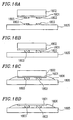
- Figures 18A-18D are cross-sectional views showing steps of a conventional method for fabricating a semiconductor device.
- Pb/Sn solders 1803 are provided in a predetermined pattern on a CMOS transistor 1805 formed on a Si substrate (not shown) and on a light modulator 1801 formed on a GaAs substrate 1802 , respectively.
- the GaAs substrate 1802 is removed by wet etching.
- the epoxy resin 1806 between the CMOS transistor 1805 and the light modulator 1801 serves as a layer for protecting the surface of the light modulator 1801 from an etchant.
- an antireflection film (not shown) is deposited on the surface of the light modulator 1801 after the GaAs substrate 1802 has been removed.
- the gap between the light modulator 1801 and the CMOS transistor 1805 is filled with the epoxy resin 1806 having a reduced viscosity.
- the heating temperature it is necessary to precisely control the heating temperature.
- voids i,e., very small bubbles
- the surface of the light modulator 1801 may be damaged.
- the present invention provides a method for fabricating a semiconductor device in which a semiconductor chip, having a first surface and a second surface substantially parallel to each other, is mounted on a submount such that the first surface faces the submount.
- the method includes: a first step of applying resin to at least one of the semiconductor chip and the submount; a second step of applying a pressure to the semiconductor chip and the submount so that the semiconductor chip and the submount are bonded to each other by the resin, resulting in electrical connection therebetween; and a third step of performing at least one of a film formation process, an etching process, a patterning process, and a washing process for the second surface of the semiconductor chip.
- a step of inspecting operational characteristics of the semiconductor chip may be further performed between the second step and the third step.
- Another semiconductor element may be formed on the second surface of the semiconductor chip in the third step.
- the method may further include, after the third step: a fourth step of removing an oxide film generated on the second surface; and a fifth step of performing an atomic layer bonding of another semiconductor chip onto the second surface of the semiconductor chip.
- another semiconductor element may be formed on the second surface of the semiconductor chip in the fifth step.
- the method may further include a step of disposing a plurality of the semiconductor chips on the submount substantially at the same time.
- the method may further include the steps of: forming a region of a metal having a low melting point on at least one of the first surface of the semiconductor chip and the submount; and heating the metal to a temperature close to the melting point thereof.
- the invention described herein makes possible the advantage of providing a method for fabricating a semiconductor device which is capable of efficiently processing the back surface of a semiconductor chip.
- Figure 1 is a general view of a semiconductor device 10 fabricated according to the method in Embodiment 1 of the present invention.
- each of the surface emitting laser chips 100 has two surfaces substantially parallel to each other.
- One of the two surfaces of the surface emitting laser chip 100 (which may be referred to as the "front surface") is in contact with the surface of the Si submount 200 .
- the "back surface” of the surface emitting laser chip 100 herein refers to the other surface of these two surfaces, which is not in contact with the Si submount 200 .
- back surface guide holes 106 through which a laser beam emitted from a surface emitting laser travels (hereinafter, simply referred to as the "guide holes 106 ") are provided.
- the guide holes 106 prevent the generated laser beam from being absorbed or scattered by the GaAs substrate on which the surface emitting laser chips 100 are formed.
- the guide hole 106 is formed in a concentric manner with the surface emitting laser formed on the front surface of the GaAs substrate. Therefore, when an optical fiber is to be coupled with the surface emitting laser, the guide hole 106 enables the alignment therebetween to be easily performed.
- the guide holes 106 are formed on the back surface of the surface emitting laser chip 100 after the surface emitting laser chip 100 is mounted on the Si submount 200 .
- a surface emitting laser to be described later is formed on the GaAs substrate so as to have an outer rim substantially in a circle.
- a diameter of the circle is, for example, in the range of about 5 ⁇ m to about 50 ⁇ m.
- a diameter of the guide hole 106 is typically set to be at about 130 ⁇ m, since a diameter of the optical fiber to be inserted into the guide hole 106 is typically about 125 ⁇ m with a margin of 5 ⁇ m.
- Figures 2A-2C are cross-sectional views explaining one of the surface emitting laser chips 100 included in the semiconductor device 10 fabricated according to the method in Embodiment 1 of the present invention.
- Wirings 204 are formed in a predetermined pattern on a Si substrate 202 of the Si submount 200 .
- the wirings 204 may be formed of, for example, a Au layer, or a plurality of metal layers including a Au layer.
- the material constituting the wirings 204 is not limited thereto.
- the surface emitting laser chip 100 is mounted on the Si submount 200 by flip chip mounting technique.
- the surface emitting laser chip 100 includes the GaAs substrate 102 and the surface emitting laser 120 provided on the GaAs substrate 102 .
- the surface emitting laser 120 includes: a p-type Bragg reflector 130 provided on the GaAs substrate 102 via an etching stop layer 104 ; an active layer 140 ; an n-type Bragg reflector 160 ; and an electrode 170 .
- the p-type Bragg reflector 130 is structured, as shown in Figure 2B , by laminating 24.5 pairs of a p-AlAs layer 132 and a p-GaAs layer 134 .
- the n-type Bragg reflector 160 has the same structure as that of the p-type Bragg reflector 130 , except that it has the n-type conductivity.
- the active layer 140 includes, as shown in Figure 2C : an n-AlGaAs layer 142 ; an AlGaAs layer 144 ; a GaAs layer 146 ; an InGaAs layer 148 ; a GaAs layer 150 ; an AlGaAs layer 152 ; and a p-AlGaAs layer 154 .
- Light generated in the active layer 140 is confined by the p-type Bragg reflector 130 and the n-type Bragg reflector 160 , thereby causing laser oscillation.
- the structure of the surface emitting laser 120 is not limited to the one which includes the p-type Bragg reflector 130 in the above-described manner, the active layer 140 and the n-type Bragg reflector 160 .
- the present invention can be applied to any surface emitting laser having at least an active layer and two reflectors interposing the active layer therebetween.
- a microbump 180 and a common anode microbump 190 are also formed on the GaAs substrate 102 so that the surface emitting laser 120 does not directly contact the Si substrate 202 upon performing the flip chip mounting. More specifically, a distance between the surface emitting laser 120 and the Si substrate 202 substantially equals the thickness of the wirings 204 , which is, for example, in the range of about 0.5 ⁇ m to about 3 ⁇ m.
- the surface emitting laser 120 is electrically connected to the microbump 180 via a Ti/Au wiring 182 .
- the Ti/Au wiring 182 may have a two-layered structure including a Ti layer and a Au layer, since it requires a certain level of mechanical strength and a low electrical resistance.
- the material constituting the wiring 182 is not limited thereto.
- Alternative materials for the Ti/Au wiring 182 include, for example, Ti, Au, Pt/Au, Ti/Pt, the combination thereof, and a TiN alloy.
- the antireflection film 108 is then deposited on an emission portion for the laser beam (i.e., in the guide hole 106 ) and on the GaAs substrate 102 .
- the guide hole 106 utilizes the etching stop layer 104 as its bottom surface.
- Each side surface of the guide hole 106 preferably has a shape of an inverted truncated cone.
- An angle formed by the generating line of the inverted truncated cone and the GaAs substrate 102 is preferably in the range of about 70° to about 85°.
- the shape of the guide hole 106 may be cylindrical.
- the space between the surface emitting laser chip 100 and the Si submount 200 is substantially filled with a UV curable resin 300 .
- the UV curable resin 300 prevents the surface of the surface emitting laser 120 from contacting the air. Accordingly, deterioration in the characteristics of the surface emitting laser 120 over time can be prevented.
- Figures 3A-3I and 4A-4C are views for illustrating steps of the method for fabricating a semiconductor device according to Embodiment 1 of the present invention, following the order of the illustration from Figure 3A to Figure 4C .
- the Si substrate 202 is pretreated in which the Si substrate 202 is typically washed with water or organic solvent.
- the wirings 204 formed of a Au layer, or a plurality of metal layers including Au, are provided in a predetermined pattern on the pretreated Si substrate 202 , thereby forming the Si submount 200 .
- the wirings 204 are intended to electrically connect the microbump 180 in the surface emitting laser chip 100 with a pad (not shown) on the Si submount 200 .
- the pad and a connecting pin Prior to the sealing of the semiconductor device 10 in a package, the pad and a connecting pin are electrically connected to each other by wire bonding.
- the Si submount 200 including the wirings 204 formed thereon is then washed with water and dried, so as to remove a foreign material on the surface of the Si submount 200 .
- the Si submount 200 may be washed with organic solvent instead of water.
- the UV curable resin 300 in a liquid form is applied to the Si submount 200 .
- the "application” herein means adhesion of the UV curable resin 300 in such a manner that the desired area on the Si submount 200 is covered therewith.
- the "application” in the present specification includes the adhesion by spraying, dropping, or the like.
- the etching stop layer 104 and crystal growth layers 124 are formed on the GaAs substrate 102 in this order using, e.g., a molecular beam epitaxy (MBE) method or a metal organic vapor phase epitaxy (MOVPE) method.
- MBE molecular beam epitaxy
- MOVPE metal organic vapor phase epitaxy
- the electrodes 170 in a predetermined array pattern are formed on the crystal growth layers 124 .
- the surface emitting laser 120 , the microbump 180 , and the common anode microbump 190 are then formed by dry-etching the crystal growth layers 124 with a mixed gas of chlorine and argon using the electrodes 170 as masks.
- the microbump 180 and the common anode microbump 190 are preferably provided with dry etching, the method is not limited thereto. For example, wet etching using a mixed solution of sulfuric acid, hydrogen peroxide solution and water may be employed.
- the surface emitting laser 120 and the microbump 180 are electrically connected to each other using the Ti/Au wiring 182 , thereby completing the surface emitting laser chip 100 .
- the surface emitting laser chip 100 is washed with water and then dried, so as to remove foreign material on the surface thereof.
- the attached material is an organic material
- the surface emitting laser chip 100 may be washed with organic solvent instead of water.
- one of, or preferably a plurality of, the surface emitting laser chips 100 are disposed so as to face the Si submount 200 , and alignment therebetween is performed.
- the surface emitting laser chips 100 are fixed on an adsorption tool 400 having inlets 402 in such a manner that the back surface of the respective chips 100 is vacuum-adsorbed to the tool 400 .
- the Si submount 200 onto which the UV curable resin 300 is dropped is fixed on an adsorption seating 410 having inlets 412 by vacuum adsorption.
- the inlets 402 and 412 are in communication with a vacuum pump (not shown), and adsorb the surface emitting laser chip 100 and the Si submount 200 , respectively, by negative pressure In the subsequent drawings, however, the inlets 402 and 412 are not shown for the purpose of simplification.
- the area of the adsorption tool 400 is typically greater than the area of the respective surface emitting laser chips 100 , so that a plurality of the surface emitting laser chips 100 can be adsorbed onto the single adsorption tool 400 , whereas the Si submount 200 with the wirings 204 corresponding to the plurality of the surface emitting laser chips 100 is adsorbed onto the adsorption seating 410 .
- the number of the surface emitting laser chips 100 to be adsorbed onto the adsorption tool 400 is preferably about 10 or greater. Alternatively, the number of the surface emitting laser chips 100 may be one.
- the surface emitting laser chips 100 and the Si submount 200 are irradiated with UV rays while being applied with pressures in directions adjacent to the surface emitting laser chips 100 and the Si submount 200 , respectively.
- the adsorption tool 400 and the adsorption seating 410 are not shown for the purpose of simplification.
- the adsorption tool 400 may be pressed against the adsorption seating 410 .
- the resin 300 which is present between the microbump 180 and the wirings 204 as well as between the cathode microbump 190 and the wirings 204 is extruded therefrom.
- the surface emitting laser chips 100 and the Si submount 200 are electrically connected to each other, and the UV curable resin 300 fills the space between the laser chips 100 and the submount 200 so as to substantially cover the surface of the surface emitting laser chips 100 opposing to the Si submount 200 .
- the pressure preferably in the range of about 3 ⁇ 10 4 N/m 2 to about 2 ⁇ 10 6 N/m 2 , and more preferably in the range of about 5 ⁇ 10 4 N/m 2 to about 7 ⁇ 10 4 N/m 2 , is applied.
- the pressure is typically applied for a period of about 20 seconds to about 10 minutes.
- the GaAs substrate 102 in the surface emitting laser chip 100 is etched away with a mixed solution of sulfuric acid, hydrogen peroxide and water. The etching is stopped when a remaining thickness of the GaAs substrate 102 becomes about 15 ⁇ m.
- the inspection is performed by operating the surface emitting laser 120 to emit light while a probe of a tester (i.e., a characteristics inspection apparatus) is allowed to stand on the wiring on the Si submount 200 electrically connected to the microbump 180 or the cathode microbump 190 , or on an inspection pad (not shown).
- a probe of a tester i.e., a characteristics inspection apparatus
- the light emitting condition of the surface emitting laser 120 is monitored by a photodetector (not shown).
- a photodetector not shown.
- the operational characteristics of the surface emitting laser 120 can be checked with the surface emitting laser chip 100 mounted on the Si submount 200 .
- the surface emitting laser chip 100 which is determined to include the surface emitting laser 120 failing to exhibit a desired characteristics as a result of this inspection process is eliminated from the subsequent fabrication process after the step in Figure 4C .
- a SiO 2 film 310 is deposited on the back surfaces of the surface emitting laser chips 100 . Thereafter, the SiO 2 film 310 is processed in a predetermined pattern with the process using normal photoresist.
- the GaAs substrate 102 with a thickness of about 15 ⁇ m is etched by reactive ion beam etching with chlorine gas, using the SiO 2 film 310 as a mask.
- the reactive ion beam etching is stopped at the etching stop layer 104 .
- the guide hole 106 is formed on the back surface of the etching stop layer 104 opposing to the surface emitting laser 120 .
- the antireflection film 108 is deposited on the back surface of the surface emitting laser chip 100 .
- the antireflection film 108 is provided in order to efficiently emit the laser beam from the surface emitting laser 120 .
- the Si submount 200 on which the integrated surface emitting laser chip 100 is mounted is divided into pieces along the scribe lines.
- the Si submount 200 including the plurality of surface emitting laser chips 100 is obtained as a single chip.
- the Si submount 200 including the single surface emitting laser chip 100 is obtained as a single chip.
- a non-defective chip is mounted onto a package and electrically connected to an external pin by a metal wire. Finally, the package is sealed.
- the guide hole 106 prevents the output light from being absorbed or scattered by the substrate, and further facilitates the coupling between the optical fiber and the surface emitting laser 120 .
- etching is performed in the step of Figure 3I ; patterning is performed in the step of Figure 4A ; and etching is performed in the step of Figure 4B .
- the present invention is not limited thereto. The advantages of the present invention can be obtained when at least any one of the film formation process, the etching process, the patterning process, and the washing process is performed with respect to the back surface which is opposite to the surface of the surface emitting laser chip 100 facing the Si submount 200 .
- the "film formation” may typically mean a film deposition by MBE or MOVPE, but is not limited thereto.
- a dielectric film, an oxide film, or an antireflection film, for example is formed.
- the "etching" herein includes the step of removing the entire film(s) formed on a wafer, and the step of selectively removing a portion excluding an area covered with a resist pattern formed typically by lithography technique.
- the etching herein includes wet etching by chemicals (e.g., an acid) and dry etching performed in a gas.
- the "patterning” herein includes the step of using a designed circuit pattern as a mask and the resist step where the mask pattern is transferred onto the wafer.
- the "washing” typically means the step of removing foreign material on a surface with water.
- the washing may be performed with organic solvent.
- drying step may be performed along with the washing.
- a microbump bonding (hereinafter, simply referred to as a "MBB") process typically including the steps shown in Figures 3A-3H , at least one of the film formation process, the etching process, the patterning process, and the washing process is performed for the back surface which is opposite to the surface of the surface emitting laser chip 100 facing the Si submount 200 .
- the back surfaces of the large number for example, in the order of about 100 to about 1000
- uniform operational characteristics, increased fabrication yield, and lower fabrication cost can be realized.
- the back surfaces of the semiconductor chips are treated, it is only necessary to fix the submount on which the semiconductor chips are mounted, rather than the semiconductor chip itself. Thus, alignment accuracy required in the production system is significantly relaxed, thereby realizing more efficient production.
- the present invention is not limited thereto.
- a plurality of field effect transistors, MOS transistors, or bipolar transistors may be formed.
- the material for the submount is typically Si, but not limited thereto.
- Figure 5 is a cross-sectional view showing one of surface emitting laser chips 100 included in a semiconductor device 20 fabricated according to the method in Embodiment 2 of the present invention.
- the semiconductor device 20 has the same structure as that of the semiconductor device 10 in Embodiment 1, except that the surface emitting laser chip 100 and the Si submount 200 are bonded to each other by fusion of microbumps 302 and 304 , and the UV curable resin 300 is not employed.
- Like components are designated with like reference numerals, and the descriptions thereof will be omitted herein.
- Figures 6A-6I and 7A-7C are views for illustrating steps in the method for fabricating a semiconductor device according to Embodiment 2 of the present invention.
- the microbumps 304 are formed on the wirings 204 .
- the microbump 302 is formed on the Ti/Au wiring 182 .
- Bismuth (Bi) may be used as a material for the microbumps 302 and 304 in Embodiment 2, but is not limited thereto. Any metal capable of fusing at such a sufficiently low temperature that a semiconductor device to be formed on the GaAs substrate 102 is not adversely affected can be used for forming the microbumps 302 and 304 . Taking this into consideration, a metal with a low melting point of about 200°C or lower is preferably used. For example, a microbump employing indium (In) may be used.
- the microbump employing Bi or In may be disposed either on the surface emitting laser chip or on the Si submount, or on both of them.
- the UV curable resin 300 is employed and irradiated with the UV rays so that the surface emitting laser chip 100 and the Si submount 200 are bonded to each other.
- the microbump 302 and the microbump 304 are heated so as to be fused and bonded to each other without use of the UV curable resin in the step of Figure 6H .
- the surface emitting laser chip 100 and the Si submount 200 are heated while being applied with pressures in directions adjacent to the surface emitting laser chip 100 and the Si submount 200 , respectively.
- the heating is performed under such conditions of temperature and time that the microbump 302 and the microbump 304 are fused.
- the microbump 302 and the microbump 304 are fused and electrically connected to each other when heated at a temperature of about 150°C for about five minutes with a pressure of about 3 ⁇ 10 4 N/m 2 .
- resist 301 is applied to those surfaces. Since the resist 301 is not intended to be used for bonding the surface emitting laser chip 100 and the Si submount 200 to each other, the resist 301 is not necessarily a UV curable resin.
- the resist 301 is typically removed using acetone.
- polyimide (not shown), for example, may be injected into the space.
- Embodiment 2 of the present invention as in Embodiment 1, at least one of the film formation process, the etching process, the patterning process, and the washing process can be simultaneously performed for the back surfaces of the large number of the surface emitting laser chips 100 .
- Figure 8 is a perspective view showing a semiconductor device 30 fabricated according to the method in Embodiment 3 of the present invention.
- Embodiment 3 of the present invention is the same as Embodiment 1, except that a Fresnel lens 110 is formed on the GaAs substrate 102 , instead of forming the guide holes 106 , in the steps shown in Figures 4A-4C in Embodiment 1.
- the GaAs substrate 102 is bonded onto the Si submount 200 by the UV curable resin 300 .
- the Fresnel lens 110 is provided on the GaAs substrate 102 .
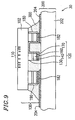
- Figure 9 is a cross-sectional view of the semiconductor device 30 fabricated according to the method in Embodiment 3 of the present invention.
- the Fresnel lens 110 is provided on the GaAs substrate 102 , i.e., on the back surface of the surface emitting laser chip 100 , so as to correspond to the center of the surface emitting laser 120 .
- Laser beam output from the surface emitting laser 120 is diffracted by the Fresnel lens 110 so as to be collected at a point (although not shown, referred to as the "light collecting point") located at a desired distance from the GaAs substrate 102 . Therefore, when an optical fiber, a photodetector, or the like, is to be deposed at the light collecting point, the output laser beam can be easily coupled to the optical fiber at a high efficiency, or the output laser beam can be easily detected at a high efficiency.
- Embodiment 3 of the present invention after etching the back surface of the surface emitting laser chip 100 in the step shown in Figure 3I described in connection with Embodiment 1, the Fresnel lens 110 is formed.
- PMMA polymethylmethacrylate
- the PMMA layer is irradiated with electron beams so as to photosensitize the PMMA layer in a pattern corresponding to the configuration of the Fresnel lens 110 to be formed.
- etching is performed with a mixed solution of saturated bromine solution and alcohol, so as to form grooves constituting the Fresnel lens 110 .
- the Fresnel lens 110 instead of the mixed solution of saturated bromine solution and alcohol used in the above for forming the Fresnel lens 110 , other materials (for example: a mixed solution of sulfuric acid, hydrogen peroxide and water; or a mixed solution of ammonia, hydrogen peroxide and water) may be used. Moreover, instead of such wet etching, dry etching using a chlorine type gas may be employed.
- Figures 8 and 9 show only one surface emitting laser chip 100
- the semiconductor device 30 can include a plurality of the laser chips 100 . In such a case, the production efficiency can be improved by simultaneously treating the large number of semiconductor chips 100 , as in Embodiment 1.
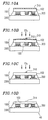
- Figures 10A-10D show some of the steps, which are different from the corresponding steps in Embodiment 1, in the method for fabricating the semiconductor device 40 according to Embodiment 4 of the present invention.
- Like components are designated with like reference numerals.
- points different from Embodiment 1 will be mainly described, and the description for the components and steps similar to the previously-explained ones will be omitted.
- the steps of Figures 3A-3I as explained in connection with Embodiment 1 are performed.
- the GaAs substrate 102 in the surface emitting laser chip 100 is etched with a mixed solution of sulfuric acid, hydrogen peroxide and water so as to have a remaining thickness of about 100 ⁇ m.
- the SiO 2 film 310 is deposited on the back surface of the surface emitting laser chip 100 .
- resist 312 is formed and patterned so as to correspond to the center of the surface emitting laser 120 .
- the pattern of the resist 312 is transferred onto the SiO 2 film 310 using tetracarbon fluoride (CF 4 ) gas.
- the back surface protrusion 314 By using the back surface protrusion 314 , coupling between the optical fiber (in which a core thereof is previously removed by 15 ⁇ m from the cut surface) and the surface emitting laser chip 100 can be realized with high accuracy and without performing alignment.
- the back surface protrusion 314 preferably has a shape of a truncated cone, which enables the optical fiber to be easily and accurately guided to a desired position in the surface emitting laser chip 100 .
- back surface protrusion 314 is formed for one surface emitting laser chip 100 in the above, a plurality of the back surface protrusions may be provided for one surface emitting laser chip 100 .
- Figures 11A-11I and 12A-12C show steps of the method for fabricating the semiconductor device 50 according to Embodiment 5 of the present invention.
- the steps shown in Figures 11A-11I respectively correspond to the steps shown in Figures 3A-3I described previously in connection with Embodiment 1.
- Like components are designated with like reference numerals. Thus, points different from Embodiment 1 will be mainly described hereinafter, and the description for the components and steps similar to the previously-explained ones will be omitted.
- a photodiode 320 is formed on the Si substrate 202 .
- the UV curable resin 300 is applied onto the Si substrate 202 so as to cover the photodiode 320 .
- the SiO 2 film 310 is deposited on the back surface of the surface emitting laser chip 100 .
- resist 322 is patterned while side walls of the resist 322 are patterned so as to have a slope of about 45° (i.e., to be processed into the "edged surface").
- the pattern of the resist 322 is transferred onto the SiO 2 film 310 so as to form an optical wave guide 324 .
- a thickness of the optical wave guide 324 i,e., a thickness of the SiO 2 film 310 is preferably in the range of about 0.01 ⁇ m to about 10 ⁇ m.
- a width of the optical wave guide 324 is preferably in the range of about 3 ⁇ m to about 50 ⁇ m.
- the optical wave guide 324 may be formed of the SiO 2 film, but is not limited thereto. Any material having a refractive index greater than that of the GaAs substrate 104 and being capable of easily guiding laser beam may be used. For example, polyimide may be used as an organic material, and AlGaAs may be employed as a semiconductor material.
- edged surfaces of the resist 322 each have a slope of about 45° as shown in Figure 12B
- the edged surfaces of the optical wave guide 324 also have a slope of about 45° after the completion of the dry etching process using tetracarbon fluoride gas as shown in Figure 12C .
- One of the edged surfaces of the optical wave guide 324 with a slope of about 45° faces the surface emitting laser 120
- the other edged surface faces the photodiode 320 .
- the optical wave guide 324 is formed on the back surface of the surface emitting laser chip 100 so as to face the surface emitting laser 120 .
- the optical wave guide 324 allows the light emitted from the surface emitting laser 120 to guide therethrough and be incident onto the photodiode 320 .
- the laser beam output from the surface emitting laser 120 transmits through the etching stop layer 104 and is incident on the edged surface of the optical wave guide 324 . Since the edged surface has a slope of about 45°, part of the beam is reflected thereon so as to be guided through the optical wave guide 324 , while the remaining part of the beam is output to the outside.
- the guided laser beam reaches the other edged surface of the optical wave guide 324 so that part of the guided beam is reflected again and is incident on the photodiode 320 .
- a signal from the photodiode 320 through the Si submount 200 to realize a feedback control for the surface emitting laser 120 it becomes possible to control the intensity of the laser beam output from the surface emitting laser 120 so as to be maintained at a constant level.
- the angle made by the edged surfaces of the resist 322 and the optical wave guide 324 is about 45°.
- any different angle except for 90° may be used, since it is only necessary for part of the laser beam output from the surface emitting laser to be reflected at the edged surface of the optical wave guide 324 and propagated through the optical wave guide 324 .
- an angle of the edged surface of the optical waveguide 324 is preferably in the range of about 30° to about 70°.
- one photodiode 320 receives only the laser beam emitted from one surface emitting laser 120 in the above explanation, the present invention is not limited thereto.
- the optical wave guide is provided such that one photodiode receives the laser beams respectively emitted from a plurality of surface emitting lasers, the laser beam output from the plurality of the surface emitting lasers can be detected as a whole at the photodiode.
- Figures 13A-13J show steps of the method for fabricating the semiconductor device 60 according to Embodiment 6 of the present invention. Like components are designated with like reference numerals. Thus, points different from Embodiment 1 will be mainly described hereinafter, and the description for the components and steps similar to the previously-explained ones will be omitted.
- the laser beam is not significantly absorbed or scattered by the GaAs substrate 102 , it is not necessary to completely remove the GaAs substrate 102 . Rather, it is sufficient to perform the etching for removing the GaAs substrate 102 by controlling the etching time so as to leave about 1/10 of the original thickness of the GaAs substrate 102 , without providing the etching stop layer 104 .
- an antireflection film 330 is deposited on the back surface of the surface emitting laser chip 100 .
- the antireflection film 330 is formed on the back surface of the surface emitting laser chip 100 which functions as an output surface (an emission portion) for the laser beam.
- the light reflection is suppressed at the back surface of the substrate, thereby being capable of efficiently emitting the laser beam.
- the amount of the laser beam which returns to the active layer is reduced, thereby eliminating the adverse effects caused by the returned light noise and an external cavity mode to be generated between the Bragg reflector and the back surface of the substrate.
- Figure 14 is a cross-sectional view showing one of surface emitting laser chips 100 included in a semiconductor device 70 fabricated according to the method in Embodiment 7 of the present invention.
- elements different from those in Embodiment 1 will be mainly described hereinafter.
- Like elements are designated with like reference numerals, and the description therefor will be omitted.
- the semiconductor device 70 includes a SEL/HBT chip 500 provided on the Si submount 200 .
- the SEL/HBT chip 500 includes a surface emitting laser 530 and a heterojunction bipolar transistor 540 provided on the same GaAs substrate 102 .
- An emitter 542 , a base 544 , and a collector 546 of the heterojunction bipolar transistor 540 are provided in this order on the GaAs substrate 102 .
- the n-type Bragg reflector 160 , the active layer 140 , the p-type Bragg reflector 130 , and the electrode 170 of the surface emitting laser 530 are provided in this order.
- the collector 546 of the heterojunction bipolar transistor 540 is electrically connected to the n-type Bragg reflector 160 of the surface emitting laser 530 .
- an electric signal input to the base 544 of the heterojunction bipolar transistor 540 is amplified by the heterojunction bipolar transistor 540 and then supplied to the surface emitting laser 530 .
- the semiconductor device 70 can perform the amplification of the input electric signal in addition to the output of the laser beam.
- the microbump 180 , a base microbump 550 , and a common cathode microbump 560 are formed on the GaAs substrate 102 such that a SEL/HBT chip 520 does not contact the Si submount 200 upon performing the flip chip mounting.
- the electrode 170 and the microbump 180 , as well as the base 544 and the base microbump 550 , are electrically connected to each other by the Ti/Au wirings 182 .
- the GaAs substrate 102 is etched away so as to have a remaining thickness of about 100 ⁇ m.
- Figures 15A-15I show steps of the method for fabricating a semiconductor device according to Embodiment 7 of the present invention.
- points different from Embodiment 1 will be mainly described.
- the description for the steps similar to the previously-explained steps will be omitted.
- the microbump 180 , the SEL/HBT 520 , the base microbump 550 , and the common cathode microbump 560 are formed on the GaAs substrate 102 , and the electrode 170 is further formed thereon.
- the GaAs substrate 102 is etched away in the step of Figure 15I , but in a different manner from Embodiment 1, so as to have a remaining thickness of about 100 ⁇ m. With such a reduced remaining thickness of the GaAs substrate 102 , the adverse effects typically caused by the scattering and absorption of the output laser beam in the GaAs substrate 102 can be reduced. As a result, the laser beam can be emitted at a high efficiency.
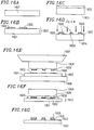
- FIG. 16A-16G and 17A-17I show steps of the method for fabricating the semiconductor device 80 according to Embodiment 8 of the present invention.
- Embodiment 8 differs from Embodiment 1 in that electrical connection is achieved by a microbump employing gold (Au) instead of the microbump employing Bi in Embodiment 2; and a film is deposited on the back surface of a surface emitting laser chip using atomic layer junction technique after the mounting of the chip.
- Au gold
- pre-treatment is performed for a Si substrate 1601 in which the Si substrate 1601 is, for example, washed with organic solvent such as acetone.
- organic solvent such as acetone.
- a wiring 1602 typically having a layered structure including an Au layer is formed in a desired pattern on the Si substrate 1601 , thereby completing a Si submount 1603 .
- an n-type Bragg reflector 1605 is grown on a GaAs substrate 1604 using a molecular beam epitaxy (MBE) method or a metal organic vapor phase epitaxy (MOVPE) method.
- MBE molecular beam epitaxy
- MOVPE metal organic vapor phase epitaxy
- the n-type Bragg reflector 1605 has the n-type conductivity, and is formed of a plurality of layers which are made of two kinds of materials having different refractive indexes.
- a Au bump 1606 is formed on the n-type Bragg reflector 1605 .
- the n-type Bragg reflector 1605 and the Au bump 1606 are etched away by dry etching with a mixed gas of chlorine and argon using the Au bump 1606 as a mask, so as to reach the GaAs substrate 1604 .
- the Si submount 1603 and the GaAs substrate 1604 are mounted. Alignment therebetween is performed while the Si submount 1603 is fixed onto an adsorption seating 1608 so as to face the GaAs substrate 1604 with the back surface thereof being vacuum-adsorbed onto an adsorption tool 1607 .
- the wiring 1602 and the Au bump 1606 are electrically connected to each other by the application of pressure in the step of Figure 16F .
- the Si submount 1603 and the GaAs substrate 1604 are heated to a temperature of about 400°C or greater while being applied with the pressure, so as to form a Au-Au junction between the wiring 1602 and the Au bump 1606 .
- a bump using different metal other than Au may be employed to realize the electrical connection between the wiring 1602 and the bump 1606 .
- resist 1609 is injected between the n-type Bragg reflector 1605 and the Si substrate 1601 of the Si submount 1603 , and then cured.
- the GaAs substrate 1604 is removed with a mixed solution of sulfuric acid, hydrogen peroxide and water. After further removing an oxide film on the back surface of the n-type Bragg reflector 1605 with hydrofluoric acid, the resist 1609 is removed.
- Figure 17A shows the state after the step in Figure 16G is completed.
- an InGaAsP active layer 1705 is grown on an InP substrate 1704 using MOVPE method.
- the Si submount 1603 (on which the n-type Bragg reflector 1605 is mounted via the Au bump 1606 ) and the InP substrate 1704 (on which the InGaAsP active layer 1705 is grown) are disposed so as to face each other, and then made closely contacted to each other.
- about several hundred grams of molybdenum (not shown) are put on the back surface of the InP substrate 1704 as a weight. While maintaining such a state, heating is performed at a temperature of about 500°C or greater in a reducing atmosphere so as to realize the atomic layer bonding between the n-type Bragg reflector 1605 and the InGaAsP active layer 1705 .
- resist 1706 is injected between the Si substrate 1601 and the InGaAsP active layer 1705 , and then cured.
- the InP substrate 1704 is then removed with a mixed solution of hydrochloric acid and phosphoric acid to obtain a bonded submount 1701 .
- the resist 1706 is removed.
- a p-type Bragg reflector 1708 is grown on a GaAs substrate 1707 using MBE method or MOVPE method.
- the bonded submount 1701 (on which the InGaAsP active layer 1705 and the n-type Bragg reflector 1605 are mounted) and the GaAs substrate 1707 are disposed so as to face each other, and made closely contacted to each other.
- about several hundred grams of molybdenum (not shown) are again put on the back surface of the GaAs substrate 1707 as a weight. While maintaining such a state, heating is performed at a temperature of about 500°C or greater in a reducing atmosphere so as to realize the atomic layer bonding between the InGaAsP active layer 1705 and the p-type Bragg reflector 1708 .
- resist 1709 is injected between the Si substrate 1601 and the InGaAsP active layer 1705 of the bonded submount 1701 , and then cured. Then, the GaAs substrate 1707 is etched away with a mixed solution of sulfuric acid, hydrogen peroxide, and water so as to have a remaining thickness of about 100 ⁇ m or less. After further removing the resist 1709 , the semiconductor device 80 is obtained as shown in Figure 17I .
- the atomic layer bonding technique By using the atomic layer bonding technique in the above-described manner, it is possible to fabricate a surface emitting laser for optical communication which is structured by a Bragg reflector with a high reflectivity. Thus, a surface emitting laser for optical communication with a reduced threshold current can be realized.
- the application of the atomic layer bonding technique to the method for fabricating a semiconductor device according to the present invention makes it possible to fabricate a surface emitting laser which can be simultaneously produced in a greater number and has less variation in characteristics, as compared to the case where a single surface emitting laser is fabricated using the atomic layer junction technique.
- a semiconductor device other than the surface emitting laser for example, a photodetector for measuring and controlling the intensity of laser beam
- the surface emitting laser and the photodetector for controlling laser beam intensity for example, can be integrated so as to be formed on the same submount.
- InGaAsP is used for the active layer of the surface emitting laser in the present embodiment, other semiconductor material such as InGaAs, GaInNAs, and InGaN may be employed.
- the present invention is described in the context of the combination of the surface emitting laser and the Si submount in each of the above-described embodiments, another electronic device such as a field effect transistor, heterojunction bipolar transistor, HEMT, and MOS transistor may be mounted on the Si submount.
- the material for the submount is not limited to silicon (Si).
- Si silicon
- glass or aluminum nitride (AlN) may be used.
- specific conditions, such as a deposited film thickness are described for illustrative purpose only, and the present invention is not limited thereto.
- one or more certain processing steps i.e., the film formation process, the etching process, the patterning process, or the washing process
- the back surfaces of the large number of the semiconductor chips can be simultaneously processed. Consequently, the large number of the semiconductor chips are processed in the same step.
- the conventional technique it is difficult to mount a semiconductor chip onto a submount after the back surface thereof is processed.
- the present invention on the other hand, it is easily realized to mount a semiconductor chip onto a submount after the back surface thereof is processed.
- the above-described feature is especially advantageous when the submount is far larger than the size of the semiconductor chip.
Landscapes
- Physics & Mathematics (AREA)
- Condensed Matter Physics & Semiconductors (AREA)
- General Physics & Mathematics (AREA)
- Electromagnetism (AREA)
- Optics & Photonics (AREA)
- Semiconductor Lasers (AREA)
- Die Bonding (AREA)
- Wire Bonding (AREA)
Applications Claiming Priority (3)
| Application Number | Priority Date | Filing Date | Title |
|---|---|---|---|
| JP13890397 | 1997-05-28 | ||
| JP138903/97 | 1997-05-28 | ||
| JP9138903A JPH10335383A (ja) | 1997-05-28 | 1997-05-28 | 半導体装置の製造方法 |
Publications (2)
| Publication Number | Publication Date |
|---|---|
| EP0881671A2 true EP0881671A2 (fr) | 1998-12-02 |
| EP0881671A3 EP0881671A3 (fr) | 1999-06-30 |
Family
ID=15232832
Family Applications (1)
| Application Number | Title | Priority Date | Filing Date |
|---|---|---|---|
| EP98109536A Withdrawn EP0881671A3 (fr) | 1997-05-28 | 1998-05-26 | Méthode de fabrication d'un dispositif semiconducteur |
Country Status (3)
| Country | Link |
|---|---|
| US (2) | US6184066B1 (fr) |
| EP (1) | EP0881671A3 (fr) |
| JP (1) | JPH10335383A (fr) |
Cited By (11)
| Publication number | Priority date | Publication date | Assignee | Title |
|---|---|---|---|---|
| WO2001080285A3 (fr) * | 2000-04-12 | 2002-02-07 | Honeywell Int Inc | Dispositifs optoelectroniques a eclairage vertical comportant des circuits integres micro-optiques et electroniques |
| WO2002071560A3 (fr) * | 2001-03-06 | 2004-02-19 | Digital Optics Corp | Separation de modules integres optiques et structures ainsi formees |
| US6709607B2 (en) | 1996-12-31 | 2004-03-23 | Honeywell International Inc. | Flexible optic connector assembly |
| US6872983B2 (en) | 2002-11-11 | 2005-03-29 | Finisar Corporation | High speed optical transceiver package using heterogeneous integration |
| EP1094511A3 (fr) * | 1999-10-22 | 2005-09-07 | Lucent Technologies Inc. | Empaquetage pour circuit intégré à profil bas |
| EP1363371A3 (fr) * | 2002-04-26 | 2006-02-22 | Fuji Xerox Co., Ltd. | Laser semiconducteur à emission de surface et son procédé de fabrication |
| US7224856B2 (en) | 2001-10-23 | 2007-05-29 | Digital Optics Corporation | Wafer based optical chassis and associated methods |
| US7961989B2 (en) | 2001-10-23 | 2011-06-14 | Tessera North America, Inc. | Optical chassis, camera having an optical chassis, and associated methods |
| EP2887388A1 (fr) * | 2013-12-03 | 2015-06-24 | Forelux Inc. | Module optoélectronique intégré |
| US9142743B2 (en) | 2011-08-02 | 2015-09-22 | Kabushiki Kaisha Toshiba | High temperature gold-free wafer bonding for light emitting diodes |
| EP2669963A4 (fr) * | 2011-01-28 | 2015-12-23 | Seoul Viosys Co Ltd | Boîtier de diode électroluminescente sur tranche et son procédé de production |
Families Citing this family (78)
| Publication number | Priority date | Publication date | Assignee | Title |
|---|---|---|---|---|
| JP3064998B2 (ja) * | 1997-10-28 | 2000-07-12 | 日本電気株式会社 | 半導体装置及びその製造方法 |
| US6730541B2 (en) * | 1997-11-20 | 2004-05-04 | Texas Instruments Incorporated | Wafer-scale assembly of chip-size packages |
| US6379577B2 (en) * | 1999-06-10 | 2002-04-30 | International Business Machines Corporation | Hydrogen peroxide and acid etchant for a wet etch process |
| US6337265B1 (en) * | 1999-09-03 | 2002-01-08 | Teraconnect, Inc. | Method for integration of integrated circuit devices |
| US6461891B1 (en) | 1999-09-13 | 2002-10-08 | Intel Corporation | Method of constructing an electronic assembly having an indium thermal couple and an electronic assembly having an indium thermal couple |
| US6576505B2 (en) * | 1999-11-25 | 2003-06-10 | Imec, Vzw | Method for transferring and stacking of semiconductor devices |
| US6344664B1 (en) * | 1999-12-02 | 2002-02-05 | Tera Connect Inc. | Electro-optical transceiver system with controlled lateral leakage and method of making it |
| JP3735526B2 (ja) * | 2000-10-04 | 2006-01-18 | 日本電気株式会社 | 半導体装置及びその製造方法 |
| US6780682B2 (en) * | 2001-02-27 | 2004-08-24 | Chippac, Inc. | Process for precise encapsulation of flip chip interconnects |
| JP4778627B2 (ja) * | 2001-04-04 | 2011-09-21 | シチズンファインテックミヨタ株式会社 | レーザダイオード用サブマウント及びその製造方法 |
| US6775308B2 (en) | 2001-06-29 | 2004-08-10 | Xanoptix, Inc. | Multi-wavelength semiconductor laser arrays and applications thereof |
| US6753197B2 (en) | 2001-06-29 | 2004-06-22 | Xanoptix, Inc. | Opto-electronic device integration |
| US6633421B2 (en) | 2001-06-29 | 2003-10-14 | Xanoptrix, Inc. | Integrated arrays of modulators and lasers on electronics |
| US6724794B2 (en) * | 2001-06-29 | 2004-04-20 | Xanoptix, Inc. | Opto-electronic device integration |
| US6790691B2 (en) | 2001-06-29 | 2004-09-14 | Xanoptix, Inc. | Opto-electronic device integration |
| US6753199B2 (en) * | 2001-06-29 | 2004-06-22 | Xanoptix, Inc. | Topside active optical device apparatus and method |
| US7831151B2 (en) * | 2001-06-29 | 2010-11-09 | John Trezza | Redundant optical device array |
| KR100918512B1 (ko) * | 2001-06-29 | 2009-09-24 | 큐빅 웨이퍼 인코포레이티드 | 광전자 소자 집적 |
| US6620642B2 (en) * | 2001-06-29 | 2003-09-16 | Xanoptix, Inc. | Opto-electronic device integration |
| US6731665B2 (en) | 2001-06-29 | 2004-05-04 | Xanoptix Inc. | Laser arrays for high power fiber amplifier pumps |
| US6504242B1 (en) | 2001-11-15 | 2003-01-07 | Intel Corporation | Electronic assembly having a wetting layer on a thermally conductive heat spreader |
| JP4054958B2 (ja) * | 2001-12-18 | 2008-03-05 | セイコーエプソン株式会社 | 発光装置、光モジュール、表示装置、光伝送装置 |
| US7068511B1 (en) * | 2001-12-31 | 2006-06-27 | Richard S. Norman | High-density architecture for a microelectronic complex on a planar body |
| US20040021214A1 (en) * | 2002-04-16 | 2004-02-05 | Avner Badehi | Electro-optic integrated circuits with connectors and methods for the production thereof |
| JP3885677B2 (ja) | 2002-07-10 | 2007-02-21 | 富士ゼロックス株式会社 | 面発光型半導体レーザ及びその製造方法ならびにその製造装置 |
| KR100512361B1 (ko) * | 2002-12-09 | 2005-09-02 | 엘지이노텍 주식회사 | 링 형태의 메사 구조를 갖는 대면적 플립칩 led |
| JP2005129776A (ja) * | 2003-10-24 | 2005-05-19 | Hamamatsu Photonics Kk | 半導体受光素子 |
| JP4279650B2 (ja) * | 2003-10-24 | 2009-06-17 | 浜松ホトニクス株式会社 | 半導体受光素子 |
| JPWO2005067062A1 (ja) * | 2003-12-26 | 2007-12-20 | 日本電気株式会社 | 光入力付基板、光出力付基板、光入出力付基板及びこれらの製造方法、光素子一体型半導体集積回路 |
| JPWO2005067061A1 (ja) * | 2003-12-26 | 2007-12-20 | 日本電気株式会社 | 光素子一体型半導体集積回路及びその製造方法 |
| KR101217590B1 (ko) * | 2004-09-22 | 2013-01-03 | 오스람 옵토 세미컨덕터스 게엠베하 | 히트 싱크 상에서 측면으로 광학적으로 펌핑된 표면발광반도체 레이저 |
| US7786592B2 (en) | 2005-06-14 | 2010-08-31 | John Trezza | Chip capacitive coupling |
| US7946331B2 (en) * | 2005-06-14 | 2011-05-24 | Cufer Asset Ltd. L.L.C. | Pin-type chip tooling |
| US7534722B2 (en) | 2005-06-14 | 2009-05-19 | John Trezza | Back-to-front via process |
| US7767493B2 (en) * | 2005-06-14 | 2010-08-03 | John Trezza | Post & penetration interconnection |
| US7838997B2 (en) * | 2005-06-14 | 2010-11-23 | John Trezza | Remote chip attachment |
| US20060278996A1 (en) * | 2005-06-14 | 2006-12-14 | John Trezza | Active packaging |
| US7687400B2 (en) * | 2005-06-14 | 2010-03-30 | John Trezza | Side stacking apparatus and method |
| US7851348B2 (en) * | 2005-06-14 | 2010-12-14 | Abhay Misra | Routingless chip architecture |
| US8456015B2 (en) * | 2005-06-14 | 2013-06-04 | Cufer Asset Ltd. L.L.C. | Triaxial through-chip connection |
| US7781886B2 (en) * | 2005-06-14 | 2010-08-24 | John Trezza | Electronic chip contact structure |
| US7521806B2 (en) * | 2005-06-14 | 2009-04-21 | John Trezza | Chip spanning connection |
| US20060281303A1 (en) * | 2005-06-14 | 2006-12-14 | John Trezza | Tack & fuse chip bonding |
| US7560813B2 (en) | 2005-06-14 | 2009-07-14 | John Trezza | Chip-based thermo-stack |
| TWI284332B (en) * | 2005-07-06 | 2007-07-21 | Monolithic Power Systems Inc | Equalizing discharge lamp currents in circuits |
| JP4466503B2 (ja) | 2005-08-08 | 2010-05-26 | ソニー株式会社 | 半導体レーザ |
| CN101341600B (zh) * | 2005-12-26 | 2012-11-28 | 日本电气株式会社 | 半导体光学元件 |
| US7687397B2 (en) * | 2006-06-06 | 2010-03-30 | John Trezza | Front-end processed wafer having through-chip connections |
| US20070281460A1 (en) * | 2006-06-06 | 2007-12-06 | Cubic Wafer, Inc. | Front-end processed wafer having through-chip connections |
| EP1906496B1 (fr) * | 2006-09-29 | 2010-01-06 | OSRAM Opto Semiconductors GmbH | Laser semi-conducteur et son procédé de fabrication |
| KR101175393B1 (ko) * | 2006-10-17 | 2012-08-20 | 쿠퍼 에셋 엘티디. 엘.엘.씨. | 웨이퍼 비아 형성 |
| US7705613B2 (en) * | 2007-01-03 | 2010-04-27 | Abhay Misra | Sensitivity capacitive sensor |
| GB2446611B (en) * | 2007-02-14 | 2011-08-17 | Bookham Technology Plc | Low creep metallization for optoelectronic applications |
| US7670874B2 (en) | 2007-02-16 | 2010-03-02 | John Trezza | Plated pillar package formation |
| US7748116B2 (en) * | 2007-04-05 | 2010-07-06 | John Trezza | Mobile binding in an electronic connection |
| US7850060B2 (en) * | 2007-04-05 | 2010-12-14 | John Trezza | Heat cycle-able connection |
| US7960210B2 (en) * | 2007-04-23 | 2011-06-14 | Cufer Asset Ltd. L.L.C. | Ultra-thin chip packaging |
| JP2009071140A (ja) * | 2007-09-14 | 2009-04-02 | Canon Inc | 面発光型デバイス |
| DE102008008595A1 (de) * | 2007-12-21 | 2009-06-25 | Osram Opto Semiconductors Gmbh | Oberflächenemittierender Halbleiterlaser und Verfahren zu dessen Herstellung |
| DE102008009108A1 (de) * | 2008-02-14 | 2009-08-20 | Osram Opto Semiconductors Gmbh | Verfahren zur Herstellung eines Halbleiterlasers sowie Halbleiterlaser |
| US7951648B2 (en) * | 2008-07-01 | 2011-05-31 | International Business Machines Corporation | Chip-level underfill method of manufacture |
| US8797057B2 (en) | 2011-02-11 | 2014-08-05 | Taiwan Semiconductor Manufacturing Company, Ltd. | Testing of semiconductor chips with microbumps |
| JP6362026B2 (ja) * | 2014-05-13 | 2018-07-25 | 株式会社リコー | レーザ装置、レーザ加工機及び表示装置 |
| JP6205088B1 (ja) * | 2014-09-25 | 2017-09-27 | コーニンクレッカ フィリップス エヌ ヴェKoninklijke Philips N.V. | 垂直共振器面発光レーザ |
| DE102017127920A1 (de) | 2017-01-26 | 2018-07-26 | Taiwan Semiconductor Manufacturing Company, Ltd. | Erhöhte Durchkontaktierung für Anschlüsse auf unterschiedlichen Ebenen |
| US11374384B2 (en) | 2017-05-31 | 2022-06-28 | Sony Corporation | Light-emitting device and method of manufacturing light-emitting device |
| JP7021829B2 (ja) * | 2017-08-14 | 2022-02-17 | ルメンタム・オペレーションズ・リミテッド・ライアビリティ・カンパニー | 表面実装対応可能なvcselアレイ |
| US10833483B2 (en) * | 2017-12-07 | 2020-11-10 | Lumentum Operations Llc | Emitter array having structure for submount attachment |
| JP2019134019A (ja) * | 2018-01-30 | 2019-08-08 | セイコーエプソン株式会社 | 発光装置 |
| US10622302B2 (en) | 2018-02-14 | 2020-04-14 | Taiwan Semiconductor Manufacturing Company, Ltd. | Via for semiconductor device connection and methods of forming the same |
| DE102018126130B4 (de) | 2018-06-08 | 2023-08-10 | Taiwan Semiconductor Manufacturing Co., Ltd. | Halbleitervorrichtung und -verfahren |
| US11158775B2 (en) | 2018-06-08 | 2021-10-26 | Taiwan Semiconductor Manufacturing Company, Ltd. | Semiconductor device and method |
| US10992100B2 (en) * | 2018-07-06 | 2021-04-27 | Taiwan Semiconductor Manufacturing Company, Ltd. | Semiconductor device and method |
| TWI701882B (zh) * | 2018-11-08 | 2020-08-11 | 晶智達光電股份有限公司 | 雷射元件 |
| CN215377954U (zh) * | 2021-03-12 | 2021-12-31 | 三赢科技(深圳)有限公司 | Vcsel器件 |
| US11557874B2 (en) * | 2021-05-18 | 2023-01-17 | Trumpf Photonics, Inc. | Double-sided cooling of laser diodes |
| US11876343B2 (en) | 2021-05-18 | 2024-01-16 | Trumpf Photonics, Inc. | Laser diode packaging platforms |
| US20230085957A1 (en) * | 2021-09-22 | 2023-03-23 | Apple Inc. | Integrated optical transceiver |
Family Cites Families (19)
| Publication number | Priority date | Publication date | Assignee | Title |
|---|---|---|---|---|
| US4749120A (en) * | 1986-12-18 | 1988-06-07 | Matsushita Electric Industrial Co., Ltd. | Method of connecting a semiconductor device to a wiring board |
| JP2657214B2 (ja) * | 1988-08-05 | 1997-09-24 | 科学技術振興事業団 | 面発光レーザ素子の製造方法 |
| US5130531A (en) * | 1989-06-09 | 1992-07-14 | Omron Corporation | Reflective photosensor and semiconductor light emitting apparatus each using micro Fresnel lens |
| US5202754A (en) * | 1991-09-13 | 1993-04-13 | International Business Machines Corporation | Three-dimensional multichip packages and methods of fabrication |
| US5270261A (en) * | 1991-09-13 | 1993-12-14 | International Business Machines Corporation | Three dimensional multichip package methods of fabrication |
| US5234153A (en) * | 1992-08-28 | 1993-08-10 | At&T Bell Laboratories | Permanent metallic bonding method |
| US5434426A (en) * | 1992-09-10 | 1995-07-18 | Kabushiki Kaisha Toshiba | Optical interconnection device |
| US5436503A (en) * | 1992-11-18 | 1995-07-25 | Matsushita Electronics Corporation | Semiconductor device and method of manufacturing the same |
| JP3484543B2 (ja) * | 1993-03-24 | 2004-01-06 | 富士通株式会社 | 光結合部材の製造方法及び光装置 |
| US5517754A (en) * | 1994-06-02 | 1996-05-21 | International Business Machines Corporation | Fabrication processes for monolithic electronic modules |
| US5796714A (en) * | 1994-09-28 | 1998-08-18 | Matsushita Electric Industrial Co., Ltd. | Optical module having a vertical-cavity surface-emitting laser |
| JP3658426B2 (ja) * | 1995-01-23 | 2005-06-08 | 株式会社日立製作所 | 光半導体装置 |
| KR0181615B1 (ko) * | 1995-01-30 | 1999-04-15 | 모리시다 요이치 | 반도체 장치의 실장체, 그 실장방법 및 실장용 밀봉재 |
| US5513204A (en) * | 1995-04-12 | 1996-04-30 | Optical Concepts, Inc. | Long wavelength, vertical cavity surface emitting laser with vertically integrated optical pump |
| JPH09260552A (ja) * | 1996-03-22 | 1997-10-03 | Nec Corp | 半導体チップの実装構造 |
| US5866953A (en) * | 1996-05-24 | 1999-02-02 | Micron Technology, Inc. | Packaged die on PCB with heat sink encapsulant |
| US5774614A (en) * | 1996-07-16 | 1998-06-30 | Gilliland; Patrick B. | Optoelectronic coupling and method of making same |
| US5925898A (en) * | 1996-07-18 | 1999-07-20 | Siemens Aktiengesellschaft | Optoelectronic transducer and production methods |
| US6016027A (en) * | 1997-05-19 | 2000-01-18 | The Board Of Trustees Of The University Of Illinois | Microdischarge lamp |
-
1997
- 1997-05-28 JP JP9138903A patent/JPH10335383A/ja not_active Withdrawn
-
1998
- 1998-05-26 EP EP98109536A patent/EP0881671A3/fr not_active Withdrawn
- 1998-05-27 US US09/085,545 patent/US6184066B1/en not_active Expired - Fee Related
-
2000
- 2000-08-16 US US09/640,280 patent/US6423561B1/en not_active Expired - Fee Related
Cited By (18)
| Publication number | Priority date | Publication date | Assignee | Title |
|---|---|---|---|---|
| US6709607B2 (en) | 1996-12-31 | 2004-03-23 | Honeywell International Inc. | Flexible optic connector assembly |
| EP1094511A3 (fr) * | 1999-10-22 | 2005-09-07 | Lucent Technologies Inc. | Empaquetage pour circuit intégré à profil bas |
| US6586776B1 (en) | 2000-04-12 | 2003-07-01 | Honeywell International Inc. | Top-emitting and top-illuminated optoelectronic integrated circuit device |
| US6780661B1 (en) | 2000-04-12 | 2004-08-24 | Finisar Corporation | Integration of top-emitting and top-illuminated optoelectronic devices with micro-optic and electronic integrated circuits |
| WO2001080285A3 (fr) * | 2000-04-12 | 2002-02-07 | Honeywell Int Inc | Dispositifs optoelectroniques a eclairage vertical comportant des circuits integres micro-optiques et electroniques |
| US7208771B2 (en) | 2001-03-06 | 2007-04-24 | Digital Optics Corporation | Separating of optical integrated modules and structures formed thereby |
| WO2002071560A3 (fr) * | 2001-03-06 | 2004-02-19 | Digital Optics Corp | Separation de modules integres optiques et structures ainsi formees |
| US7751659B2 (en) | 2001-10-23 | 2010-07-06 | Tessera North America, Inc. | Optical apparatus |
| US7224856B2 (en) | 2001-10-23 | 2007-05-29 | Digital Optics Corporation | Wafer based optical chassis and associated methods |
| US7961989B2 (en) | 2001-10-23 | 2011-06-14 | Tessera North America, Inc. | Optical chassis, camera having an optical chassis, and associated methods |
| US8233757B2 (en) | 2001-10-23 | 2012-07-31 | Digitaloptics Corporation East | Wafer based optical chassis and associated methods |
| US7058104B2 (en) | 2002-04-26 | 2006-06-06 | Fuji Xerox Co., Ltd. | Surface emitting semiconductor laser and method of fabricating the same |
| EP1363371A3 (fr) * | 2002-04-26 | 2006-02-22 | Fuji Xerox Co., Ltd. | Laser semiconducteur à emission de surface et son procédé de fabrication |
| US7306959B2 (en) | 2002-11-11 | 2007-12-11 | Finisar Corporation | Methods of fabricating integrated optoelectronic devices |
| US6872983B2 (en) | 2002-11-11 | 2005-03-29 | Finisar Corporation | High speed optical transceiver package using heterogeneous integration |
| EP2669963A4 (fr) * | 2011-01-28 | 2015-12-23 | Seoul Viosys Co Ltd | Boîtier de diode électroluminescente sur tranche et son procédé de production |
| US9142743B2 (en) | 2011-08-02 | 2015-09-22 | Kabushiki Kaisha Toshiba | High temperature gold-free wafer bonding for light emitting diodes |
| EP2887388A1 (fr) * | 2013-12-03 | 2015-06-24 | Forelux Inc. | Module optoélectronique intégré |
Also Published As
| Publication number | Publication date |
|---|---|
| JPH10335383A (ja) | 1998-12-18 |
| US6184066B1 (en) | 2001-02-06 |
| EP0881671A3 (fr) | 1999-06-30 |
| US6423561B1 (en) | 2002-07-23 |
Similar Documents
| Publication | Publication Date | Title |
|---|---|---|
| US6423561B1 (en) | Method for fabricating semiconductor device | |
| US6999493B2 (en) | Surface emission laser and manufacturing method for surface emission laser, light reception element and manufacturing method for light reception element, and optical transceiver module | |
| US6444491B1 (en) | Composite semiconductor devices and method for manufacture thereof | |
| KR101195311B1 (ko) | 반도체 발광 소자 및 그 제조 방법 | |
| EP0704947B1 (fr) | Module optique avec un laser à semi-conducteur à émission de surface à cavité verticale | |
| US6658041B2 (en) | Wafer bonded vertical cavity surface emitting laser systems | |
| US6368890B1 (en) | Top contact VCSEL with monitor | |
| US6674948B2 (en) | Optoelectronic IC module | |
| US9859681B2 (en) | Optical device and light irradiation apparatus | |
| US6692979B2 (en) | Methods of fabricating optoelectronic IC modules | |
| WO2021124968A1 (fr) | Élément laser à émission par la surface à cavité verticale, réseau d'éléments laser à émission par la surface à cavité verticale, module laser à émission par la surface à cavité verticale et procédé de fabrication d'élément laser à émission par la surface à cavité verticale | |
| JP6536004B2 (ja) | 面発光レーザ装置及びその製造方法 | |
| JP2002368334A (ja) | 面発光レーザ、フォトダイオード、それらの製造方法及びそれらを用いた光電気混載回路 | |
| US20030031218A1 (en) | VCSEL structure and method of making same | |
| US5906753A (en) | Method of making optical semi-conductor device | |
| JP3941713B2 (ja) | 面発光レーザを備えた半導体集積回路、半導体集積回路の製造方法および電子機器 | |
| JPH09223848A (ja) | 半導体集積回路 | |
| JP4643891B2 (ja) | パラレル光学系接続装置用の位置決め方法 | |
| CN114765338A (zh) | 将微透镜应用于小孔径光电检测器和vcsel上以用于高数据速率应用的方法 | |
| US8178364B2 (en) | Testing method of surface-emitting laser device and testing device thereof | |
| JP2002057283A (ja) | 半導体集積回路の製造方法 | |
| US20250201735A1 (en) | Optical semiconductor device and method for manufacturing optical semiconductor device | |
| Goossen et al. | 1/spl times/12 VCSEL array with optical monitoring via flip-chip bonding | |
| Zhang et al. | Micro-transfer-printed III-V-on-silicon C-band Distributed Bragg Reflector Laser | |
| JP2005093722A (ja) | 光機能素子および光機能素子の製造方法 |
Legal Events
| Date | Code | Title | Description |
|---|---|---|---|
| PUAI | Public reference made under article 153(3) epc to a published international application that has entered the european phase |
Free format text: ORIGINAL CODE: 0009012 |
|
| AK | Designated contracting states |
Kind code of ref document: A2 Designated state(s): DE FR GB NL |
|
| AX | Request for extension of the european patent |
Free format text: AL;LT;LV;MK;RO;SI |
|
| 17P | Request for examination filed |
Effective date: 19981110 |
|
| PUAL | Search report despatched |
Free format text: ORIGINAL CODE: 0009013 |
|
| RIC1 | Information provided on ipc code assigned before grant |
Free format text: 6H 01L 21/70 A, 6H 01L 21/77 B, 6H 01L 21/98 B, 6H 01L 33/00 B, 6H 01S 3/025 B, 6H 01S 3/25 B |
|
| AK | Designated contracting states |
Kind code of ref document: A3 Designated state(s): AT BE CH CY DE DK ES FI FR GB GR IE IT LI LU MC NL PT SE |
|
| AX | Request for extension of the european patent |
Free format text: AL;LT;LV;MK;RO;SI |
|
| AKX | Designation fees paid |
Free format text: DE FR GB NL |
|
| 17Q | First examination report despatched |
Effective date: 20031029 |
|
| RAP1 | Party data changed (applicant data changed or rights of an application transferred) |
Owner name: PANASONIC CORPORATION |
|
| STAA | Information on the status of an ep patent application or granted ep patent |
Free format text: STATUS: THE APPLICATION IS DEEMED TO BE WITHDRAWN |
|
| 18D | Application deemed to be withdrawn |
Effective date: 20091201 |