EP0881871A2 - Schmales Kabelmodem und dessen Halter - Google Patents
Schmales Kabelmodem und dessen Halter Download PDFInfo
- Publication number
- EP0881871A2 EP0881871A2 EP98304243A EP98304243A EP0881871A2 EP 0881871 A2 EP0881871 A2 EP 0881871A2 EP 98304243 A EP98304243 A EP 98304243A EP 98304243 A EP98304243 A EP 98304243A EP 0881871 A2 EP0881871 A2 EP 0881871A2
- Authority
- EP
- European Patent Office
- Prior art keywords
- housing
- section
- face
- circuit board
- cable modem
- Prior art date
- Legal status (The legal status is an assumption and is not a legal conclusion. Google has not performed a legal analysis and makes no representation as to the accuracy of the status listed.)
- Granted
Links
Images




Classifications
-
- H—ELECTRICITY
- H05—ELECTRIC TECHNIQUES NOT OTHERWISE PROVIDED FOR
- H05K—PRINTED CIRCUITS; CASINGS OR CONSTRUCTIONAL DETAILS OF ELECTRIC APPARATUS; MANUFACTURE OF ASSEMBLAGES OF ELECTRICAL COMPONENTS
- H05K7/00—Constructional details common to different types of electric apparatus
- H05K7/20—Modifications to facilitate cooling, ventilating, or heating
-
- H—ELECTRICITY
- H05—ELECTRIC TECHNIQUES NOT OTHERWISE PROVIDED FOR
- H05K—PRINTED CIRCUITS; CASINGS OR CONSTRUCTIONAL DETAILS OF ELECTRIC APPARATUS; MANUFACTURE OF ASSEMBLAGES OF ELECTRICAL COMPONENTS
- H05K5/00—Casings, cabinets or drawers for electric apparatus
- H05K5/0017—Casings, cabinets or drawers for electric apparatus with operator interface units
-
- H—ELECTRICITY
- H05—ELECTRIC TECHNIQUES NOT OTHERWISE PROVIDED FOR
- H05K—PRINTED CIRCUITS; CASINGS OR CONSTRUCTIONAL DETAILS OF ELECTRIC APPARATUS; MANUFACTURE OF ASSEMBLAGES OF ELECTRICAL COMPONENTS
- H05K7/00—Constructional details common to different types of electric apparatus
- H05K7/20—Modifications to facilitate cooling, ventilating, or heating
- H05K7/20009—Modifications to facilitate cooling, ventilating, or heating using a gaseous coolant in electronic enclosures
-
- Y—GENERAL TAGGING OF NEW TECHNOLOGICAL DEVELOPMENTS; GENERAL TAGGING OF CROSS-SECTIONAL TECHNOLOGIES SPANNING OVER SEVERAL SECTIONS OF THE IPC; TECHNICAL SUBJECTS COVERED BY FORMER USPC CROSS-REFERENCE ART COLLECTIONS [XRACs] AND DIGESTS
- Y10—TECHNICAL SUBJECTS COVERED BY FORMER USPC
- Y10S—TECHNICAL SUBJECTS COVERED BY FORMER USPC CROSS-REFERENCE ART COLLECTIONS [XRACs] AND DIGESTS
- Y10S345/00—Computer graphics processing and selective visual display systems
- Y10S345/905—Display device with housing structure
Definitions
- the present invention relates to a cable modem, as well as a stand for mounting the cable modem thereon, which is to be used as an interface for connecting a CATV (Cable Television) line and a personal computer to each other.
- CATV Consumer Television
- the cable modem has been playing an important role in recent years as an interface for high-speed data communications between CATV line and home or business equipment.
- This cable modem is equipped with an interface function of converting encoded transmission information into reception signals for personal computers.
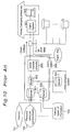
- Fig. 10 shows a schematic view of a prior art example of the cable modem system.
- Internet 101, personal computer communication 102 or various types of information 103 is transmitted via servers 201, 202 or via a server 203 other than the CATV station (e.g., a server provided within a company), and in relay of a router 204 and further through an information encoding process by a cable modem encoder 205, to each home or company or the like 300.
- This encoded information which could not be received as it is by personal computers, is subjected to signal transformation by a cable modem 301 so as to be receivable by a personal computer 302.
- the cable modem is fabricated through steps of inserting a metal plate for heat radiation between the two boards, mounting the circuit board structure with the metal plate inserted, in which the two boards and the metal plate have been connected to each other by screws, to a metallic chassis having a generally U-shaped cross section, and further housing the chassis in a box type cabinet.
- Such a cable modem would take much time in assembly and inevitably involve increased outside dimensions of the cabinet, occupying a considerable space when installed on a desk, and besides the cable modem would be heavy in unit weight so as to be inconvenient to carry. Further, when the cable modem, which is normally positioned horizontally, is positioned vertically for saving space, it would be unstable, being prone to tilt. Furthermore, as another problem, when the cable modem is of smaller size and thin type design, use environmental temperatures of the circuit components would be exceeded due to temperature increase in the interior of the cabinet, causing malfunction.
- an object of the present invention is to provide a high reliability cable modem which can be designed for thinner thickness and lighter weight as compared with the prior art, and which is superior in assembling workability, heat radiation, mounting stability and the like.
- a thin type cable modem comprising: a circuit board which is a substantially single board on which at least a front end section, a logic circuit section and an LED display section are mounted; and a housing which covers the circuit board and which has a front face, a rear face, a left side face, a right side face, a top face and a bottom face, wherein a plurality of symbol displays for indicating an operational state of the LED display section are provided in the front face of the housing, and a plurality of exhaust holes for radiating heat generated from the front end section and the logic circuit section mounted on the circuit board are provided in the top face of the housing, and wherein a plurality of inlet holes for taking outside air into an interior of the housing are provided in the bottom face of the housing, and the front end section is mounted on the circuit board at a position near the plurality of exhaust holes provided in the top face of the housing.
- Heat generated from the front end section and the logic circuit section mounted on the circuit board can be radiated efficiently along with an air stream that passes from the bottom face of the housing into the housing interior through the inlet holes and flows upward of the housing through the exhaust holes.
- the LED display section is implemented by surface-mounted LED chips and mounted on the circuit board.
- the front end section, the logic circuit section and the LED display circuit components are mounted and completed onto a substantially single board all by an automatic mounting machine, there is no need of separately preparing the front end section and LED display circuit board and the logic circuit board and thereafter combining the two boards by manual work, which would be involved in the prior art, and neither is there a need of inserting the LED lamp by hand nor, after hand soldering, cutting off leads, so that the assembly process can be omitted.
- the production cost can be reduced.
- the housing has, inside its front face, a plurality of light guide sections for guiding an optical signal, which designates an operational state, from the plurality of LED chips to the plurality of symbol displays.
- the light guide section fixed to the front panel and the LED chips for the light source are of independent structure, there is no need of positioning the front end portion of the LED lamp to a center portion of the front panel opening, so that the assembly process can be omitted. Thus, the production cost can be reduced.
- a stand for mounting a thin type cable modem which comprises: a circuit board which is a substantially single board on which at least a front end section, a logic circuit section and an LED display section are mounted; and a housing which covers the circuit board and which has a front face, a rear face, a left side face, a right side face, a top face and a bottom face, wherein a plurality of exhaust holes for radiating heat generated from the front end section and the logic circuit section mounted on the circuit board are provided in the top face of the housing, and a plurality of inlet holes for taking outside air into an interior of the housing are provided in the bottom face of the housing, the mounting stand comprising: both side walls; a housing mounting portion; a recessed portion provided in the housing mounting portion so as not to close the plurality of inlet holes provided in the bottom face of the housing; and an engaging portion which is formed in the recessed portion and which is to be engaged with the inlet holes.
- the mounting stand allows the thin type cable modem to be stably mounted thereon and, at the same time, serves also as a slide stopper for the cable modem body.
- the engaging portion of the mounting stand becomes parallel to the inlet holes so that the inlet holes and the engaging portion are engaged with each other when the bottom face of the housing having the plurality of inlet holes is mounted on the mounting stand, while the engaging portion of the mounting stand becomes non-parallel to the exhaust holes so that the exhaust holes and the engaging portion are not engaged with each other when the top face of the housing having the plurality of exhaust holes is mounted on the mounting stand.
- the housing can be prevented from being inversely mounted onto the mounting stand.
- Fig. 1 is an appearance perspective view showing a thin type cable modem according to an embodiment of the present invention in conjunction with the appended Claims 1 to 3.
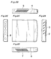
- Figs. 2A, 2B, 2C, 2D and 2E are a front face view, a top face view, a side face view, a bottom face view and a rear face view, respectively, of the cable modem.
- a plurality of symbol displays 3 for indicating operating state of an LED display section.
- a top face 4 of the housing are provided a plurality of exhaust holes 5 for radiating heat generated from a front end section and a logic circuit section mounted on a circuit board.
- a bottom face 6 of the housing there are a plurality of inlet holes 7 for taking outside air into the interior of the housing.
- a power supply cord and various connectors are connected to a rear face 8 . Outside dimensions of the housing are about 209 mm long ⁇ about 35 mm wide ⁇ about 170 mm deep.
- Fig. 3 is an arrangement diagram of circuit components mounted onto a board 9 in the housing of the cable modem, where numeral 11 denotes the front end section, 12 denotes the logic circuit section, 13 denotes the LED display section and 14 denotes a light guide section.
- This front end section 11 is mounted on a circuit board 10 located near the plurality of exhaust holes 5 provided in the top face 4 of the housing.
- the board 9 is substantially a single circuit board such as a multi-layer circuit board, a double-sided circuit board or other board of various kinds of constitution.
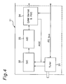
- Fig. 4 is a circuit block diagram of the front end section
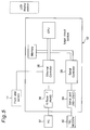
- Fig. 5 is a circuit block diagram of the logic circuit section
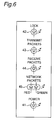
- Fig. 6 is a circuit block diagram of the LED display section. Operations of the individual circuit blocks are described with reference to the accompanying drawings.
- a desired signal is selected by a tuner 31 from among down RF data signals from a CATV station.
- An IF signal derived from the tuner is converted into a base band signal by a down converter 32, further converted from analog to digital form by an analog-to-digital converter 33, thereafter demodulated and error-corrected by a 64QAM (Quadrature Amplitude Modulation) and FEC (Forward Error Correction) 34, and after these steps, led out as a data signal.
- 64QAM Quadrature Amplitude Modulation
- FEC Forward Error Correction
- a data signal demodulated by the QAM and led out from the front end section 11 is transmitted to a personal computer 37 via an Ethernet controller 35 and through a 10 Base-T connector 36.
- a data signal derived from the personal computer 37 is led out from a serial port 39 via the Ethernet controller 35 and using the DMA (Direct Memory Access) system via a serial controller 38, and thus connected to an external telephone modem 40.
- DMA Direct Memory Access
- an LED 41 marked as POWER is lit upon power-up
- an LED 42 marked as LOCK is lit by occurrence of a clock signal from the front end section
- LEDs 43, 44 marked as TRANSMIT PACKETS, RECEIVE PACKETS are lit upon transmission and reception of a packet signal, respectively.
- an LED 45 marked as NETWORK PACKETS is lit red during the transmit and reception of packet signals, and green after the transmission and reception of packet signals (at an end of packets).
- Power consumption of the whole cable modem is 5 - 6 W in the standby state and 10 - 11 W in the operating state, thus necessitating heat radiation in both standby state and operating state.
- no cooling fan is attached, and neither is a metallic plate nor metallic chassis or the like for heat radiation provided.
- the front end section is placed in upper part of the circuit board near the exhaust holes for use of heat radiation while the logic circuit section is placed in lower part of the circuit board, in order to prevent heat accumulation in the housing interior. If the front end section was disposed in lower part of the circuit board, logic circuit components positioned above the front end section would be heated and adversely affected and moreover the whole housing interior would be increased in temperature, which would lead to some malfunction of the circuits.
- a chimney effect by making use of air flow is taken into consideration by providing a plurality of inlet holes in the bottom face of the housing. That is, heat released from the front end section and the logic circuit section goes up as it rides on an upward air stream caused by the heat, and is radiated upward of the housing through the plurality of exhaust holes provided in the top face of the housing. This upward air stream causes the internal air pressure to decrease, so that outside air flows into the interior of the housing through the plurality of inlet holes provided in the bottom face of the housing.
- the cable modem can be designed for a thin type by making it possible to mount the front end section, the logic circuit section and the LED display circuit components on a single board, which is achieved by miniaturizing the components of the front end section and the logic circuit section and by reducing the parts amount as a result of adopting an FPGA (Field Programmable Gate Array) or ASIC (Application Specific Integrated Circuit) for the logic circuit components, and besides by using a surface-mounted chip LED and further by lowering the noise level to a permissible noise level as a result of separating the power supply line for the tuner, the high-frequency section and the digital section as well as the ground line, and further forming a linear and shortest path for signal flow in the tuner, the high-frequency section and the digital section to thereby optimize the wiring pattern.
- FPGA Field Programmable Gate Array
- ASIC Application Specific Integrated Circuit
- Fig. 7 shows the structure of the LED display section, where Fig. 7A is a front perspective view and Fig. 7B is a sectional view taken along the line B - B of Fig. 7A.
- Fig. 7B light outputted from an LED chip 52 automatically mounted on a circuit board 51 by the surface mount technology becomes incident on a light guide section 53 fixed to a front panel 54, and is reflected by a tilted side face portion S of the light guide section 53, finally reaching an end portion T. Accordingly, the LED display section becomes easier to assemble, as compared with the manual mounting of the LED lamp in the prior art example.
- Fig. 8 is an appearance perspective view showing the structure of a stand for mounting the thin type cable modem according to the present invention.
- Reference numeral 60 denotes both side walls, which sandwich the housing of the cable modem therebetween.
- Numeral 61 denotes a cable modem housing mounting portion, and 62 denotes a recessed portion formed in the housing mounting portion so that the inlet holes in the bottom face of the housing are not closed.
- numeral 63 denotes an engaging portion which is formed in the recessed portion 62 of the housing mounting portion so as to be engaged with the inlet holes in the bottom face of the housing.
- Numeral 66 denotes rubber feet for prevention of vibrations and slides.
- Fig. 9 shows the positional relation between the mounting stand and the inlet/exhaust holes of the housing when the thin type cable modem of the invention is mounted on the mounting stand, where Fig. 9A shows the mounting stand, Fig. 9B shows the inlet holes in the bottom face of the housing and Fig. 9C shows the exhaust holes in the top face of the housing.
Landscapes
- Engineering & Computer Science (AREA)
- Microelectronics & Electronic Packaging (AREA)
- Physics & Mathematics (AREA)
- Thermal Sciences (AREA)
- Cooling Or The Like Of Electrical Apparatus (AREA)
- Telephonic Communication Services (AREA)
- Insertion, Bundling And Securing Of Wires For Electric Apparatuses (AREA)
Applications Claiming Priority (3)
| Application Number | Priority Date | Filing Date | Title |
|---|---|---|---|
| JP13805997A JP3323881B2 (ja) | 1997-05-28 | 1997-05-28 | 薄型ケーブルモデム及びその載置用スタンド |
| JP138059/97 | 1997-05-28 | ||
| JP13805997 | 1997-05-28 |
Publications (3)
| Publication Number | Publication Date |
|---|---|
| EP0881871A2 true EP0881871A2 (de) | 1998-12-02 |
| EP0881871A3 EP0881871A3 (de) | 1999-08-18 |
| EP0881871B1 EP0881871B1 (de) | 2004-07-21 |
Family
ID=15213025
Family Applications (1)
| Application Number | Title | Priority Date | Filing Date |
|---|---|---|---|
| EP98304243A Expired - Lifetime EP0881871B1 (de) | 1997-05-28 | 1998-05-28 | Flaches Kabelmodem und dessen Halter |
Country Status (7)
| Country | Link |
|---|---|
| US (1) | US6229507B1 (de) |
| EP (1) | EP0881871B1 (de) |
| JP (1) | JP3323881B2 (de) |
| KR (1) | KR100300690B1 (de) |
| CN (1) | CN1102332C (de) |
| DE (1) | DE69825099T2 (de) |
| TW (1) | TW454434B (de) |
Cited By (8)
| Publication number | Priority date | Publication date | Assignee | Title |
|---|---|---|---|---|
| US6590782B2 (en) | 2001-02-28 | 2003-07-08 | Adc Telecommunications, Inc. | Telecommunications chassis and card |
| WO2002096124A3 (en) * | 2001-05-18 | 2003-07-24 | Adc Telecommunications Inc | Telecommunications chassis and card |
| US6637845B2 (en) | 2001-02-28 | 2003-10-28 | Adc Telecommunications, Inc. | Telecommunications chassis and card with flame spread containment |
| WO2003089224A1 (en) * | 2002-04-19 | 2003-10-30 | Nokia Corporation | Method for fabricating a plastic molded indicator symbol and a plastic molded indicator symbol |
| WO2003019306A3 (en) * | 2001-08-24 | 2004-03-18 | Honeywell Int Inc | Controller input/output module visual indicator and safety means |
| US6940730B1 (en) | 2001-02-28 | 2005-09-06 | Adc Telecommunications, Inc. | Telecommunications chassis and card |
| EP1890430A1 (de) | 2006-08-17 | 2008-02-20 | Belkin International Inc. | Netzwerk-Hardwareelement zur Kopplung von Computernetzwerkelementen und Verfahren zur Informationsanzeige darauf |
| US7675862B2 (en) | 2006-08-17 | 2010-03-09 | Belkin International, Inc. | Networking hardware element to couple computer network elements and method of displaying a network layout map thereon |
Families Citing this family (26)
| Publication number | Priority date | Publication date | Assignee | Title |
|---|---|---|---|---|
| MY122767A (en) * | 1999-11-02 | 2006-05-31 | Matsushita Electric Industrial Co Ltd | Network connection apparatus |
| US6730889B1 (en) * | 2000-03-15 | 2004-05-04 | The Holmes Group, Inc. | Programmable slow-cooker accessory |
| US6573483B1 (en) | 2000-03-15 | 2003-06-03 | The Holmes Group, Inc. | Programmable slow-cooker appliance |
| US6987250B2 (en) * | 2000-04-28 | 2006-01-17 | The Holmes Group, Inc. | Control circuit for kitchen appliances |
| US6448899B1 (en) * | 2000-10-25 | 2002-09-10 | Nortel Networks Limited | Power indicating ethernet outlet and method therefor |
| USD452233S1 (en) | 2000-11-21 | 2001-12-18 | Novatel Wireless, Inc. | RF wireless modem |
| US6362459B1 (en) * | 2001-01-12 | 2002-03-26 | The Metal Ware Company | Electronically controlled roaster oven with digital control assembly |
| KR100411255B1 (ko) * | 2001-06-11 | 2003-12-18 | 삼성전기주식회사 | 케이블 모뎀 튜너 모듈의 히트싱크 |
| US7453693B2 (en) * | 2002-12-20 | 2008-11-18 | Allied Telesis Kabushiki Kaisha | Network device |
| CN1315361C (zh) * | 2003-06-09 | 2007-05-09 | 三星电子株式会社 | 显示器及其控制方法 |
| TWM270461U (en) * | 2005-01-07 | 2005-07-11 | Datastor Technology Co Ltd | External storage device with outward projection light source |
| CN200956692Y (zh) * | 2006-09-22 | 2007-10-03 | 鸿富锦精密工业(深圳)有限公司 | 电子设备 |
| US8651704B1 (en) | 2008-12-05 | 2014-02-18 | Musco Corporation | Solid state light fixture with cooling system with heat rejection management |
| FR2948485B1 (fr) * | 2009-07-24 | 2011-10-21 | Sagem Comm | Dispositif d'accueil pour disque dur |
| USD649151S1 (en) * | 2009-09-04 | 2011-11-22 | Netgear, Inc. | Network device having wide viewing angle indicators for performance |
| US7903405B1 (en) * | 2009-09-18 | 2011-03-08 | Fisher-Rosemount Systems, Inc. | Electronic device enclosures having improved ventilation to dissipate heat |
| USD628573S1 (en) * | 2010-05-04 | 2010-12-07 | Datastore Technology Corp. | External storage device case |
| KR101080737B1 (ko) | 2010-09-17 | 2011-11-07 | (주)동부로봇 | 다수의 조명창을 갖는 서보모터 |
| TW201225723A (en) * | 2010-12-03 | 2012-06-16 | Askey Computer Corp | Wireless network apparatus capable of illumination |
| US20130335998A1 (en) * | 2011-03-15 | 2013-12-19 | Kazuya Inoue | Electronic device and method of guiding light in the same |
| US20130291365A1 (en) * | 2012-05-03 | 2013-11-07 | Fluke Corporation | Accessory mounting system |
| EP2747533B1 (de) * | 2012-12-21 | 2017-11-29 | Minimax GmbH & Co. KG | Elektronischer Schaltschrank mit Kühlung |
| CN104320930B (zh) * | 2014-09-30 | 2017-08-08 | 深圳市理邦精密仪器股份有限公司 | 一种层叠式的超声模块布局结构 |
| USD760719S1 (en) * | 2014-10-20 | 2016-07-05 | Hand Held Products, Inc. | Scanner |
| US9436238B1 (en) * | 2015-03-09 | 2016-09-06 | Adtran, Inc. | Convection-cooled electronic system |
| CN104901721B (zh) * | 2015-05-29 | 2018-07-10 | 北京人师北清科技发展有限公司 | 一种测试cmts的猫车 |
Family Cites Families (13)
| Publication number | Priority date | Publication date | Assignee | Title |
|---|---|---|---|---|
| CA1310186C (en) * | 1988-03-31 | 1992-11-17 | Frederick Dimmick | Display sign |
| JPH0737356Y2 (ja) | 1989-03-15 | 1995-08-23 | 沖電気工業株式会社 | スタンド構造 |
| JPH0617167Y2 (ja) | 1989-04-27 | 1994-05-02 | シーケーディ株式会社 | 表示装置 |
| EP0419689B1 (de) | 1989-09-25 | 1994-06-01 | Siemens Aktiengesellschaft | Baugruppe mit einer Leiterplatte |
| US5214621A (en) | 1990-12-20 | 1993-05-25 | Square D Company | Universal circuit board housing with a hinged member |
| JP2745924B2 (ja) | 1992-01-16 | 1998-04-28 | ヤマハ株式会社 | 縦形デスクトップ機器のスタンド |
| JPH05266643A (ja) | 1992-03-19 | 1993-10-15 | Sony Corp | 外部記憶装置のスタンド |
| JPH0684487U (ja) | 1993-05-17 | 1994-12-02 | 株式会社ヤマウ | 発光標識体 |
| GB2280534B (en) * | 1993-07-30 | 1997-04-16 | Koito Mfg Co Ltd | Display device |
| US5481440A (en) * | 1993-12-27 | 1996-01-02 | At&T Corp. | Circuit pack with light pipes |
| US5760754A (en) * | 1995-12-04 | 1998-06-02 | Motorola, Inc. | Light pipe assembly and electrical device using same |
| US5623392A (en) * | 1996-06-04 | 1997-04-22 | Ma; Hsi-Kuang | LCD assembly with projection function |
| US5781411A (en) * | 1996-09-19 | 1998-07-14 | Gateway 2000, Inc. | Heat sink utilizing the chimney effect |
-
1997
- 1997-05-28 JP JP13805997A patent/JP3323881B2/ja not_active Expired - Fee Related
-
1998
- 1998-05-19 US US09/080,463 patent/US6229507B1/en not_active Expired - Fee Related
- 1998-05-21 TW TW087107875A patent/TW454434B/zh not_active IP Right Cessation
- 1998-05-27 KR KR1019980019197A patent/KR100300690B1/ko not_active Expired - Fee Related
- 1998-05-28 DE DE69825099T patent/DE69825099T2/de not_active Expired - Fee Related
- 1998-05-28 CN CN98114963A patent/CN1102332C/zh not_active Expired - Fee Related
- 1998-05-28 EP EP98304243A patent/EP0881871B1/de not_active Expired - Lifetime
Cited By (12)
| Publication number | Priority date | Publication date | Assignee | Title |
|---|---|---|---|---|
| US6590782B2 (en) | 2001-02-28 | 2003-07-08 | Adc Telecommunications, Inc. | Telecommunications chassis and card |
| US6637845B2 (en) | 2001-02-28 | 2003-10-28 | Adc Telecommunications, Inc. | Telecommunications chassis and card with flame spread containment |
| US6707686B2 (en) | 2001-02-28 | 2004-03-16 | Adc Telecommunications, Inc. | Telecommunications chassis and card |
| US6940730B1 (en) | 2001-02-28 | 2005-09-06 | Adc Telecommunications, Inc. | Telecommunications chassis and card |
| US7324348B2 (en) | 2001-02-28 | 2008-01-29 | Adc Telecommunications, Inc. | Telecommunications chassis and card |
| US7639510B2 (en) | 2001-02-28 | 2009-12-29 | Adc Telecommunications, Inc. | Telecommunications chassis having a repeater card |
| WO2002082877A3 (en) * | 2001-04-03 | 2003-08-14 | Adc Telecommunications Inc | Telecommunications chassis and card |
| WO2002096124A3 (en) * | 2001-05-18 | 2003-07-24 | Adc Telecommunications Inc | Telecommunications chassis and card |
| WO2003019306A3 (en) * | 2001-08-24 | 2004-03-18 | Honeywell Int Inc | Controller input/output module visual indicator and safety means |
| WO2003089224A1 (en) * | 2002-04-19 | 2003-10-30 | Nokia Corporation | Method for fabricating a plastic molded indicator symbol and a plastic molded indicator symbol |
| EP1890430A1 (de) | 2006-08-17 | 2008-02-20 | Belkin International Inc. | Netzwerk-Hardwareelement zur Kopplung von Computernetzwerkelementen und Verfahren zur Informationsanzeige darauf |
| US7675862B2 (en) | 2006-08-17 | 2010-03-09 | Belkin International, Inc. | Networking hardware element to couple computer network elements and method of displaying a network layout map thereon |
Also Published As
| Publication number | Publication date |
|---|---|
| KR19980087409A (ko) | 1998-12-05 |
| JPH10335864A (ja) | 1998-12-18 |
| DE69825099T2 (de) | 2005-07-21 |
| US6229507B1 (en) | 2001-05-08 |
| TW454434B (en) | 2001-09-11 |
| CN1204229A (zh) | 1999-01-06 |
| JP3323881B2 (ja) | 2002-09-09 |
| DE69825099D1 (de) | 2004-08-26 |
| KR100300690B1 (ko) | 2001-09-28 |
| CN1102332C (zh) | 2003-02-26 |
| EP0881871B1 (de) | 2004-07-21 |
| EP0881871A3 (de) | 1999-08-18 |
Similar Documents
| Publication | Publication Date | Title |
|---|---|---|
| US6229507B1 (en) | Thin type cable modem and stand for mounting the same | |
| JP5387772B2 (ja) | ファンユニット、電子機器、及びファンユニットの製造方法 | |
| US20220141949A1 (en) | Linecard system using riser printed circuit boards (pcbs) | |
| US20220303155A1 (en) | Modular physical layer and integrated connector module for local area networks | |
| JP4381038B2 (ja) | 送受信装置およびケーブルモデムモジュール装置 | |
| US20070268667A1 (en) | Air-cooling system configuration for touch screen | |
| US10305217B2 (en) | Thermally-enhanced pluggable modules | |
| WO2009057124A2 (en) | A set-top-box cabinet for natural cooling of internal electronics | |
| US6219235B1 (en) | Electronic assembly for standard rack enclosures | |
| JP2004063861A (ja) | 光通信器、光送信器、光送受信器および光伝送システム | |
| JP2016220082A (ja) | 光伝送モジュール及び伝送装置 | |
| US20020160742A1 (en) | Transmitting and amplifying unit for wireless communication device | |
| US8769808B2 (en) | Method for fixed and replaceable module architecture | |
| US20090298340A1 (en) | Common module for tab up type and tab down type network connector | |
| EP1542521B1 (de) | Elektronische Vorrichtung | |
| JP4854635B2 (ja) | ビデオカメラの放熱構造 | |
| HK1017569A (en) | Thin type cable modem and stand for mounting the same | |
| AU2005220272A1 (en) | Electronic equipment | |
| JP2015087481A (ja) | 光アンプモジュール | |
| JP5157152B2 (ja) | 電子機器 | |
| US20030043548A1 (en) | Power supply | |
| KR200359093Y1 (ko) | 데이터 통신 서버 케이스 | |
| CN216531956U (zh) | 一种电路板上元器件的保护结构 | |
| CN111031757A (zh) | 一种微波组件 | |
| JP2005108881A (ja) | 電子機器 |
Legal Events
| Date | Code | Title | Description |
|---|---|---|---|
| PUAI | Public reference made under article 153(3) epc to a published international application that has entered the european phase |
Free format text: ORIGINAL CODE: 0009012 |
|
| AK | Designated contracting states |
Kind code of ref document: A2 Designated state(s): DE FR GB |
|
| AX | Request for extension of the european patent |
Free format text: AL;LT;LV;MK;RO;SI |
|
| PUAL | Search report despatched |
Free format text: ORIGINAL CODE: 0009013 |
|
| AK | Designated contracting states |
Kind code of ref document: A3 Designated state(s): AT BE CH CY DE DK ES FI FR GB GR IE IT LI LU MC NL PT SE |
|
| AX | Request for extension of the european patent |
Free format text: AL;LT;LV;MK;RO;SI |
|
| RIC1 | Information provided on ipc code assigned before grant |
Free format text: 6H 05K 7/20 A, 6H 05K 5/00 B |
|
| 17P | Request for examination filed |
Effective date: 19991013 |
|
| AKX | Designation fees paid |
Free format text: DE FR GB |
|
| 17Q | First examination report despatched |
Effective date: 20030228 |
|
| GRAP | Despatch of communication of intention to grant a patent |
Free format text: ORIGINAL CODE: EPIDOSNIGR1 |
|
| GRAS | Grant fee paid |
Free format text: ORIGINAL CODE: EPIDOSNIGR3 |
|
| GRAA | (expected) grant |
Free format text: ORIGINAL CODE: 0009210 |
|
| AK | Designated contracting states |
Kind code of ref document: B1 Designated state(s): DE FR GB |
|
| REG | Reference to a national code |
Ref country code: GB Ref legal event code: FG4D |
|
| REF | Corresponds to: |
Ref document number: 69825099 Country of ref document: DE Date of ref document: 20040826 Kind code of ref document: P |
|
| ET | Fr: translation filed | ||
| PLBE | No opposition filed within time limit |
Free format text: ORIGINAL CODE: 0009261 |
|
| STAA | Information on the status of an ep patent application or granted ep patent |
Free format text: STATUS: NO OPPOSITION FILED WITHIN TIME LIMIT |
|
| 26N | No opposition filed |
Effective date: 20050422 |
|
| PGFP | Annual fee paid to national office [announced via postgrant information from national office to epo] |
Ref country code: DE Payment date: 20080605 Year of fee payment: 11 |
|
| PGFP | Annual fee paid to national office [announced via postgrant information from national office to epo] |
Ref country code: GB Payment date: 20080528 Year of fee payment: 11 |
|
| GBPC | Gb: european patent ceased through non-payment of renewal fee |
Effective date: 20090528 |
|
| REG | Reference to a national code |
Ref country code: FR Ref legal event code: ST Effective date: 20100129 |
|
| PG25 | Lapsed in a contracting state [announced via postgrant information from national office to epo] |
Ref country code: FR Free format text: LAPSE BECAUSE OF NON-PAYMENT OF DUE FEES Effective date: 20090602 |
|
| PGFP | Annual fee paid to national office [announced via postgrant information from national office to epo] |
Ref country code: FR Payment date: 20080514 Year of fee payment: 11 |
|
| PG25 | Lapsed in a contracting state [announced via postgrant information from national office to epo] |
Ref country code: GB Free format text: LAPSE BECAUSE OF NON-PAYMENT OF DUE FEES Effective date: 20090528 |
|
| PG25 | Lapsed in a contracting state [announced via postgrant information from national office to epo] |
Ref country code: DE Free format text: LAPSE BECAUSE OF NON-PAYMENT OF DUE FEES Effective date: 20091201 |