EP0883131A2 - Dispositif de mémoire à semiconducteurs tel que qu'une mémoire cache - Google Patents
Dispositif de mémoire à semiconducteurs tel que qu'une mémoire cache Download PDFInfo
- Publication number
- EP0883131A2 EP0883131A2 EP98110315A EP98110315A EP0883131A2 EP 0883131 A2 EP0883131 A2 EP 0883131A2 EP 98110315 A EP98110315 A EP 98110315A EP 98110315 A EP98110315 A EP 98110315A EP 0883131 A2 EP0883131 A2 EP 0883131A2
- Authority
- EP
- European Patent Office
- Prior art keywords
- memory cell
- memory cells
- data
- row
- pair
- Prior art date
- Legal status (The legal status is an assumption and is not a legal conclusion. Google has not performed a legal analysis and makes no representation as to the accuracy of the status listed.)
- Granted
Links
Images



Classifications
-
- G—PHYSICS
- G11—INFORMATION STORAGE
- G11C—STATIC STORES
- G11C11/00—Digital stores characterised by the use of particular electric or magnetic storage elements; Storage elements therefor
- G11C11/21—Digital stores characterised by the use of particular electric or magnetic storage elements; Storage elements therefor using electric elements
- G11C11/34—Digital stores characterised by the use of particular electric or magnetic storage elements; Storage elements therefor using electric elements using semiconductor devices
- G11C11/40—Digital stores characterised by the use of particular electric or magnetic storage elements; Storage elements therefor using electric elements using semiconductor devices using transistors
- G11C11/41—Digital stores characterised by the use of particular electric or magnetic storage elements; Storage elements therefor using electric elements using semiconductor devices using transistors forming static cells with positive feedback, i.e. cells not needing refreshing or charge regeneration, e.g. bistable multivibrator or Schmitt trigger
- G11C11/413—Auxiliary circuits, e.g. for addressing, decoding, driving, writing, sensing, timing or power reduction
- G11C11/417—Auxiliary circuits, e.g. for addressing, decoding, driving, writing, sensing, timing or power reduction for memory cells of the field-effect type
- G11C11/419—Read-write [R-W] circuits
-
- G—PHYSICS
- G06—COMPUTING OR CALCULATING; COUNTING
- G06F—ELECTRIC DIGITAL DATA PROCESSING
- G06F12/00—Accessing, addressing or allocating within memory systems or architectures
- G06F12/02—Addressing or allocation; Relocation
- G06F12/08—Addressing or allocation; Relocation in hierarchically structured memory systems, e.g. virtual memory systems
- G06F12/0802—Addressing of a memory level in which the access to the desired data or data block requires associative addressing means, e.g. caches
- G06F12/0804—Addressing of a memory level in which the access to the desired data or data block requires associative addressing means, e.g. caches with main memory updating
-
- Y—GENERAL TAGGING OF NEW TECHNOLOGICAL DEVELOPMENTS; GENERAL TAGGING OF CROSS-SECTIONAL TECHNOLOGIES SPANNING OVER SEVERAL SECTIONS OF THE IPC; TECHNICAL SUBJECTS COVERED BY FORMER USPC CROSS-REFERENCE ART COLLECTIONS [XRACs] AND DIGESTS
- Y02—TECHNOLOGIES OR APPLICATIONS FOR MITIGATION OR ADAPTATION AGAINST CLIMATE CHANGE
- Y02D—CLIMATE CHANGE MITIGATION TECHNOLOGIES IN INFORMATION AND COMMUNICATION TECHNOLOGIES [ICT], I.E. INFORMATION AND COMMUNICATION TECHNOLOGIES AIMING AT THE REDUCTION OF THEIR OWN ENERGY USE
- Y02D10/00—Energy efficient computing, e.g. low power processors, power management or thermal management
Definitions
- the present invention relates to improvement of a semiconductor storage device such as a cache memory.
- a recent microprocessor is generally provided with a high-speed cache memory disposed between a CPU and a low-speed main mass storage device in order to improve the entire performance.
- a cache memory is described in detail in, for example, "Computer Architecture: A Quantitative Approach” written by John L. Hennessy and David A. Patterson, published by Morgan Knafmann Publishers, Inc. (1990).
- a control system for a cache memory is basically classified into the following two systems respectively adopting different write methods: a write through (store in) system and a write back system.
- a write through system both the cache memory and the main storage device are written.
- the write back system merely the cache memory is written, and when a block in the cache memory where data has been changed is to be rewritten, the data is written in the main storage device.
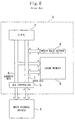
- Figure 8 illustrates such a conventional cache memory, and is a block diagram for showing an exemplified configuration of the cache memory and peripheral related equipment.
- a reference numeral 1 denotes a microprocessor, whose composing elements relating to the invention alone are shown in Figure 8 .
- a reference numeral 3 denotes a CPU
- a reference numeral 4 denotes an external main storage device
- a reference numeral 5 denotes a bus controller
- a reference numeral 6 denotes an address bus
- a reference numeral 7 denotes a data bus
- a reference numeral 8 denotes a cache memory
- a reference numeral 9 denotes a write back buffer.
- the address bus 6 transfers an address signal supplied by the CPU 3 to the cache memory 8 and also to the main storage device 4 through the bus controller 5 .
- the data bus 7 transfers data between the cache memory 8 or the main storage device 4 and the CPU 3 .
- the bus controller 5 controls the address bus 6 and the data bus 7 between the bus controller 5 and the main storage device 4 .
- a minimum unit of data transferred between the cache memory 8 and the main storage device 4 is designated as a block or a line, and the size of a block is generally larger than, for example, an integral number of times as large as a data width (bit number) of data transferred between the cache memory 8 and the data bus 7 in a batch.
- the write back buffer 9 is used for temporarily holding the data to be written back in the main storage device 4 so that waiting time can be shortened.
- the write back buffer 9 is provided as an external circuit of the cache memory 8 , and hence, the write (save) operation in the write back buffer 9 should be conducted through the data bus 7 .
- Data to be saved in the write back buffer 9 corresponds to all data of a minimum unit transferred between the cache memory 8 and the main storage device 4 , namely, all data of the block including the address to be written, and the block size is several times as large as the data width of data transferred between the cache memory 8 and the data bus 7 in a batch. Therefore, in order to save the data of one block in the write back buffer 9 , it is necessary to make several accesses to the cache memory 8 to read the data.
- the data width of data transferred between the cache memory 8 and the data bus 7 in a batch is 32 bits and the block size is 128 bits (16 bytes)
- at least four accesses should be made to the cache memory 8 in order to save the data of one block in the write back buffer 9 . Accordingly, the throughput of the entire system using the microprocessor 1 can be disadvantageously degraded.
- the write back buffer 9 is required to hold data of a block with a large size. Therefore, even when the write back buffer 9 is constructed by using, for example, a generally used flip-flop and the like, the write back buffer 9 occupies a large area, resulting in increasing the chip area.
- the objects of the invention are, in temporarily storing data necessary to be written back in a main storage device, improving throughput and decreasing consumed power by temporarily storing all the data to be written back through a smaller number of accesses, preferably through one access, to a cache memory, as well as decreasing the chip area by constructing a write back buffer or the like by using memory cells.
- the memory cell array of the cache memory of this invention is provided with a specific memory cell row for constituting a write back buffer, so that the data to be written back in the main storage device can be written and temporarily held in the specific memory cell row without using a data bus.
- the semiconductor storage device of this invention comprises a memory cell array including memory cells aligned in an array, each of the memory cells connected with each interconnection point between plural word lines extending in a row direction and plural bit line pairs extending in a column direction, and in this semiconductor storage device, one word line is selected among the plural word lines for selecting memory cells aligned in one row connected with the selected word line, and data are read from and written in the selected memory cells through bit line pairs connected with the selected memory cells, the memory cell array is provided with a specific memory cell row including at least one row of memory cells extending in the row direction, and the semiconductor storage device is further provided with writing means capable of writing all data of the memory cells aligned in one row and selected by the selected word line in the specific memory cell row through the bit line pairs connected with the selected memory cells.
- the data of the memory cells aligned in one row and selected by the selected word line are read through the bit line pairs connected with the selected memory cells regardless of an operation of the writing means, and the writing means selects the specific memory cell row in reading the data of the selected memory cell aligned in one row, and writes all the data of the selected memory cells aligned in one row in the one row of memory cells included in the specific memory cell row through the bit line pairs connected with the selected memory cells.
- the memory cells aligned in one row and included in the specific memory cell row are selected by a word line for selecting the specific memory cell row, and data of the selected memory cells included in the specific memory cell row are read through bit line pairs connected with the selected memory cells.
- the semiconductor storage device can further comprise a column switch for selecting part of plural data read in the plural bit line pairs, and the part of data selected by the column switch is externally output to a data bus of a microprocessor.
- each of the memory cells included in the specific memory cell row is constructed by using a static memory cell including a cross connection circuit having a pair of inverting devices each constructed by a serial circuit having an input terminal and an output terminal and including serially connected load device and driving MOSFET, the pair of inverting devices being cross connected with the input terminals and the output terminals of the serial circuits; at least one pair of transferring MOSFETs each disposed between each of the output terminals of the pair of inverting devices and a bit line pair; and a controlling MOSFET disposed between a shared source shared by the driving MOSFETs of the pair of inverting devices and a reference potential line and controlled to be set in an unselected state in a data write operation.
- each of the memory cells included in the specific memory cell row is constructed by using a static memory cell including a cross connection circuit having a pair of inverting devices each constructed by a serial circuit having an input terminal and an output terminal and including serially connected load device and driving MOSFET, the pair of inverting devices being cross connected with the input terminals and the output terminals of the serial circuits; at least one pair of transferring MOSFETs each disposed between each of the output terminals of the pair of inverting devices and a bit line pair; and a pair of controlling MOSFETs disposed respectively between one of the driving MOSFETs of the pair of inverting devices and a reference potential line and between the other of the driving MOSFETs and the reference potential line and controlled to be set in an unselected state in a data write operation.
- the cache memory of this invention comprises a cache memory cell array including memory cells aligned in an array, each of the memory cells connected with each intersection point between plural word lines extending in a row direction and plural bit line pairs extending in a column direction, and in this cache memory, one of the plural word lines is selected for selecting memory cells aligned in one row connected with the selected word line, and data are read from and written in the selected memory cells through bit line pairs connected with the selected memory cells, the cache memory is further provided with a write back buffer for temporarily holding data written in a part of memory cells of the cache memory cell array when the data is necessary to be written in a main storage device, the write back buffer is constituted by a specific memory cell row included in the cache memory cell array, and including at least one row of memory cells extending in the row direction, and bit line pairs connected with the memory cells of the specific memory cell row constituting the write back buffer are commonly used as the bit line pairs of the cache memory cell array.
- data of the memory cells aligned in one row selected by the selected word line are read through the bit line pairs connected with the selected memory cells regardless of selection of the specific memory cell row constituting the write back buffer, and the cache memory is further provided with writing means for selecting the specific memory cell row constituting the write back buffer when the data of the memory cells aligned in one row selected by the selected word line are read, and writing all data of the selected memory cells aligned in one row in the memory cells included in the specific memory cell row constituting the write back buffer through the bit line pairs connected with the selected memory cells.
- the memory cells aligned in one row and included in the specific memory cell row constituting the write back buffer are selected by a word line for selecting the specific memory cell row, and data of the selected memory cells aligned in one row and included in the specific memory cell row are read through bit line pairs connected with the selected memory cells.
- the cache memory can further comprises a column switch for selecting a part of plural data read in the plural bit line pairs, and the part of data selected by the column switch is externally output to a data bus of a microprocessor.
- each row of the cache memory cell array and the specific memory cell row constituting the write back buffer includes memory cells in a number equal to a number of data in a minimum unit transferred to and received from the main storage device.
- each of the memory cells included in the specific memory cell row is constructed by using a static memory cell including a cross connection circuit having a pair of inverting devices each constructed by a serial circuit having an input terminal and an output terminal and including serially connected load device and driving MOSFET, the pair of inverting devices being cross connected with the input terminals and the output terminals of the serial circuits; at least a pair of transferring MOSFETs each disposed between each of the output terminals of the pair of inverting devices and a bit line pair; and a controlling MOSFET disposed between a shared source shared by the driving MOSFETs of the pair of inverting devices and a reference potential line and controlled to be set in an unselected state in a data write operation.
- each of the memory cells included in the specific memory cell row is constructed by using a static memory cell including a cross connection circuit having a pair of inverting devices each constructed by a serial circuit having an input terminal and an output terminal and including serially connected load device and driving MOSFET, the pair of inverting devices being cross connected with the input terminals and the output terminals of the serial circuits; at least a pair of transferring MOSFETs each disposed between each of the output terminals of the pair of inverting devices and a bit line pair; and a pair of controlling MOSFETs disposed respectively between one of the driving MOSFETs of the pair of inverting devices and a reference potential line and between the other of the driving MOSFETs and the reference potential line and controlled to be set in an unselected state in a data write operation.
- all data selected by an arbitrary word line in the memory cell array can be written in the specific memory cell row through the plural bit line pairs in a batch at the same time as a read operation.
- the data output to the bit line pairs are externally output from the semiconductor storage device through the column switch, the sense circuit and the output buffer, but the number of bit line pairs which are simultaneously selected by one word line and to which the data are output is several times as large as the bit number of externally output data. Accordingly, the data of the memory cells in a number several times as large as the bit number of the externally output data can be simultaneously written or saved in the specific memory cell row in a batch.
- the driving MOSFETs included in the memory cells of the specific memory cell row are disconnected from the reference potential lines. Therefore, the data of the specific memory cell row are not output to the bit lines but the data in the memory cell array selected by the arbitrary word line are output. Moreover, storage nodes of the memory cells included in the specific memory cell row are supplied with the potential of the bit lines. In other words, when the specific memory cell row is controlled to be set in the write state, all the data of the memory cells aligned in one row selected by the arbitrary word line in the memory cell array can be written in the specific memory cell row through the bit line pairs.
- data of the memory cells in a number several times as large as the data width of data transferred between the cache memory and a data bus in a batch can be simultaneously written and saved in the write back buffer in a batch. For example, when addresses in the cache memory are set so that one block is allocated to one word line and the number of memory cells simultaneously selected by one word line is set at the same number as the block size, all the data of one block can be simultaneously saved in the write back buffer through one data read operation.
- the number of accesses to be made to the cache memory in saving data in the write back buffer can be largely decreased. Furthermore, also since the data bus is not used in saving the data in the write back buffer, the throughput of the entire system using the microprocessor can be improved and the power consumption can be decreased. Also, since the write back buffer is constructed by using the memory cells, the chip area can be simultaneously decreased.
- the cache memory of this invention when the number of data output from the cache memory to the data bus is smaller than the number of data in a minimum unit (i.e., a block) transferred between the cache memory and the main storage device, the data of one block can be saved in the write back buffer in a batch through one read operation.
- a minimum unit i.e., a block
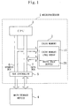
- FIG. 1 is a block diagram for showing an exemplified configuration of a cache memory according to a first embodiment of the invention and peripheral related equipment.
- a reference numeral 1 denotes a microprocessor, whose composing elements relating to the invention alone are shown in Figure 1 .
- a reference numeral 3 denotes a CPU, and a reference numeral 4 denotes an external main storage device.
- the microprocessor 1 includes, in addition to the CPU 3 , a bus controller 5 , an address bus 6 , a data bus 7 and a cache memory 2 .
- the microprocessor 1 is provided with the cache memory according to this invention (namely, the cache memory 2 ) having a write back buffer 20 included in a cache memory cell array 10 therein.
- the write back buffer 9 is used for temporarily holding the data to be written back in the low-speed main storage device 4 .
- the cache memory cell array (memory cell array) 10 of the cache memory 2 of this embodiment includes the write back buffer 20 . Therefore, in performing a write operation (save operation) in the write back buffer 20 , there is no need to use the data bus 7 , and the write operation, namely, the save operation, can be performed within the cache memory cell array 10 alone.
- Figure 2 shows an exemplified configuration of the cache memory 2 , which includes the memory cell array 10 , an address decoder 31 , a word line driver 32 , a column switch 33 , a sense circuit 34 and a data output buffer 35 .
- AD indicates an address signal input from the address bus 6
- DOUT indicates data output output to the data bus 7 .
- a clock controller, a write circuit and the like are omitted.
- a reference numeral 20 denotes a specific memory cell row or a write back buffer included in the memory cell array 10 .
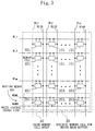
- Figure 3 shows an exemplified configuration of the cache memory cell array 10 , and the cache memory cell array 10 of Figure 3 is constructed in a matrix of m rows by n columns (wherein m and n are arbitrary integers), which does not limit the invention.
- reference numerals 101 denote plural memory cells
- reference numerals 201 denote plural memory cells included in the specific memory cell row 20
- WL1 through WLm indicates word lines
- BL1 through BLn and BL1B through BLnB indicate bit line pairs
- WBWL indicates a word line of the specific memory cell row
- WBWR indicates a write control signal line for controlling a write operation in the specific memory cell row.
- the address signal AD is decoded by the address decoder 31 , and one word line among the word lines WL1 through WLm corresponding to the address signal AD is selectively driven by the word line driver 32 , thereby outputting data in the memory cells 101 corresponding to the selected word line to the bit line pairs BL1 and BL1B through BLn and BLnB .
- n memory cells 101 are simultaneously selected, and the data are output to all the bit line pairs BL1 and BL1B through BLn and BLnB .
- the data of a part of the bit line pairs selected by the column switch 33 is amplified by the sense circuit 34 so as to be output by the data output buffer 35 .
- the word line WBWL of the specific memory cell row 20 is not selected, this operation is the same as a general read operation of a static RAM .
- the clock controller, the write circuit and the like are omitted.
- bit line pairs BL1 and BL1B through BLn and BLnB are supplied with the data from all the memory cells corresponding to one word line selected among the word lines WL1 through WLm , the data are written in all the memory cells 201 included in the specific memory cell row 20 at the same time.
- the column switch 33 selects a part of the bit line pairs, and hence, the number n of the bit line pairs is larger than the bit number of the data output DOUT .
- the number n of the bit line pairs can be 64, 128, 256, etc.
- the number n of the bit line pairs is determined in view of the delay time of the word line and a consumed current depending upon the number of bit line pairs simultaneously selected.
- the data of all the memory cells corresponding to the selected word line can be written in the specific memory cell row 20 through the bit line pairs at the same time and in a batch through one access. Furthermore, in reading the specific memory cell row 20 , the data can be read in the same manner as in reading the general memory cells 101 , with all the word lines WL1 through WLm unselected, with the word line WBWL of the specific memory cell row 20 selected, and with the write control signal line WBWR to the specific memory cell row 20 controlled to be set in the read state.
- Figure 4 shows an exemplified configuration of the general memory cell 101 , wherein WL indicates a word line, BL and BLB indicate a bit line pair, ML1 and ML2 indicate loading MOSFETs, MD1 and MD2 indicate driving MOSFETs, and MA1 and MA2 indicate transferring MOSFETs.
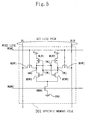
- Figure 5 shows an exemplified configuration of the memory cell 201 included in the specific memory cell row 20 , and in this example, the memory cell 201 is constituted by a static memory cell.
- WBWL indicates a word line
- BL and BLB indicate a bit line pair.
- the memory cell 201 includes a pair of inverting devices, one of which includes serial connection of a loading MOSFET (load device) MLW1 and a driving MOSFET MDW1 and the other of which includes serial connection of another loading MOSFET (load device) MLW2 and another driving MOSFET MDW2 .
- the input terminals IW1 and IW2 and the output terminals NW1 and NW2 of these inverting devices are cross connected, thereby constituting a cross connection circuit. Furthermore, between the output terminal NW1 of one inverting device and one bit line BL of the bit line pair BL and BLB , a transferring MOSFET MAW1 is interposed, and between the output terminal NW2 of the other inverting device and the other bit line BLB , a transferring MOSFET MAW2 is interposed. These transferring MOSFETs MAW1 and MAW2 are controlled by the word line WBWL . Also, MWR0 indicates a controlling MOSFET to be controlled to be unselected by the write control signal line WBWR in a write operation.
- This controlling MOSFET MWR0 is disposed between a shared source shared by the pair of driving MOSFETs MDW1 and MDW2 and a reference potential line GND .
- p-channel MOSFETs are used as the transferring MOSFETs MAW1 and MAW2 because of a bit line potential described below.
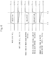
- Figure 6 shows a rough waveform in a write operation in the memory cell 201 of Figure 5 .
- the word line WL of the general memory cells 101 Through the activation (selection) of the word line WL of the general memory cells 101 , the data of the corresponding memory cells 101 are output to the bit line pairs BL and BLB . At this point, when the word line WBWL of the memory cells 201 included in the specific memory cell row 20 is deactivated (unselected), the general read operation is conducted.
- the word line WBWL of the memory cells 201 included in the specific memory cell row 20 is activated (selected) and the controlling MOSFET MWR0 is controlled to be unselected by the write control signal line WBWR . Since the controlling MOSFET MWR0 is unselected, the data storage nodes (output terminals) NW1 and NW2 of the memory cells 201 included in the specific memory cell row 20 are disconnected from the ground potential.
- the data held in the data storage nodes NW1 and NW2 are not output to the bit line pair BL and BLB , but the data output to the bit line pair BL and BLB from the general memory cell 101 are transferred to the data storage nodes NW1 and NW2 .
- the bit line pair BL and BLB are precharged to a supply voltage, and the p-channel MOSFETs are used as the transferring MOSFETs MAW1 and MAW2 , and hence, a small amplitude between the bit line pair BL and BLB close to the supply voltage can be transferred to the data storage nodes NW1 and NW2 .
- the controlling MOSFET MWR0 is controlled to be selected by using the write control signal line WBWR , and the memory cells 201 conduct the same operation as a sense circuit, so that the small amplitude close to the supply voltage between the data storage nodes NW1 and NW2 can be increased to a reference potential.
- the data can be accurately held (time t2 ).
- the data stored by the general memory cells 101 are written in the memory cells 201 .
- the word line WL of the general memory cells 101 and the word line WBWL of the memory cells 201 included in the specific memory cell row 20 can be placed in the unselected state.
- the word line WBWL of the memory cells 201 included in the specific memory cell row 20 is selected with the word line WL of the general memory cells 101 set in the unselected state and with the controlling MOSFET MWR0 selected by the write control signal line WBWR , the data in the memory cells 201 included in the specific memory cell row 20 are output to the bit line pair BL and BLB .
- the data can be read in the same manner as in the general operation.
- writing means 200 is constructed by the configuration where the word line WBWL of the memory cells 201 included in the specific memory cell row 20 is activated (selected) and the controlling MOSFET MWR0 is controlled to be unselected by the write control signal line WBWR .
- the read data can be simultaneously written in the memory cells 201 included in the specific memory cell row 20 through the bit line pairs by operating the writing means 200 .
- the semiconductor storage device is used as the cache memory in the microprocessor 1 of Figure 1 as follows:
- addresses in the cache memory 2 are set so that entire one block (namely, data in a minimum unit transferred between the cache memory and the main storage device 4 ) can be selected by the same one word line, and the number of memory cells aligned in one row and simultaneously selected by one word line is set at the same as the block size (the number of transferred data in a minimum unit). In this manner, all the data in one block can be output to the bit line pairs by selecting one word line, and the data of one block can be all saved in the write back buffer 20 simultaneously through one data read operation.
- the number of accesses to be made to the cache memory 2 can be largely decreased.
- data of all memory cells aligned in one row in the memory cell array 10 and selected by an arbitrary word line can be written in the specific memory cell row 20 through the bit line pairs in a batch at the same time as the read operation.
- the specific memory cell row 20 of this semiconductor storage device is used as the write back buffer and the semiconductor storage device is used as a cache memory in the system using the microprocessor 1 including the cache memory 2 , the number of accesses to be made to the cache memory 2 for saving data in the write back buffer 20 can be largely decreased.
- the data bus 7 is not used in the save operation in the write back buffer 20 , the throughput of the entire system using the microprocessor 1 can be improved as well as the power consumption of the microprocessor 1 can be decreased.
- the write back buffer 20 is constructed by using the memory cells, the occupied area can be simultaneously decreased.
- the specific memory cell row or write back buffer 20 has merely one row of memory cells, namely, merely one word line WBWL is used.
- the specific memory cell row or write back buffer 20 can include plural rows of memory cells.
- plural word lines WBWL are provided so as to correspond to the plural rows of the memory cells included in the specific memory cell row or write back buffer 20 , and the address decoder 31 and the word line driver 32 are used for the selection of the word lines. In this manner, data in all memory cells in plural rows selected by plural word lines WL in the memory cell array 10 can be written and saved in the plural rows of the memory cells included in the specific memory cell row or write back buffer 20 .
- the plural rows of the memory cells in the specific memory cell row 20 included in the memory cell array 10 can be used as the write back buffer.
- Figure 7 shows a modification of the memory cell 201 included in the specific memory cell row 20 shown in Figure 5 .
- FIG. 7 The configuration of Figure 7 is different from that of Figure 5 as follows: A pair of controlling MOSFETs MWR1 and MWR2 controlled to be unselected by the write control signal line WBWR are respectively serially connected between the sources of the driving MOSFETs MDW1 and MDW2 and reference potential lines GND . The rest of the configuration is the same as that of Figure 5 . Also, the operation and the effect are completely the same.
- CMOS type memory cell is used as the memory cell, which does not limit the invention.
- a high resistance type memory cell or a TFT type memory cell can be used.
- a multiport type memory cell including two or more pairs of transferring MOSFETs can be used.
Landscapes
- Engineering & Computer Science (AREA)
- Theoretical Computer Science (AREA)
- Microelectronics & Electronic Packaging (AREA)
- Computer Hardware Design (AREA)
- Physics & Mathematics (AREA)
- General Engineering & Computer Science (AREA)
- General Physics & Mathematics (AREA)
- Memory System Of A Hierarchy Structure (AREA)
- Static Random-Access Memory (AREA)
- Dram (AREA)
- Microcomputers (AREA)
Applications Claiming Priority (3)
| Application Number | Priority Date | Filing Date | Title |
|---|---|---|---|
| JP14955797 | 1997-06-06 | ||
| JP149557/97 | 1997-06-06 | ||
| JP14955797A JP3489967B2 (ja) | 1997-06-06 | 1997-06-06 | 半導体記憶装置及びキャッシュメモリ装置 |
Publications (3)
| Publication Number | Publication Date |
|---|---|
| EP0883131A2 true EP0883131A2 (fr) | 1998-12-09 |
| EP0883131A3 EP0883131A3 (fr) | 1999-12-01 |
| EP0883131B1 EP0883131B1 (fr) | 2006-01-25 |
Family
ID=15477782
Family Applications (1)
| Application Number | Title | Priority Date | Filing Date |
|---|---|---|---|
| EP98110315A Expired - Lifetime EP0883131B1 (fr) | 1997-06-06 | 1998-06-05 | Dispositif de mémoire à semiconducteurs tel que qu'une mémoire cache |
Country Status (5)
| Country | Link |
|---|---|
| US (1) | US6304943B1 (fr) |
| EP (1) | EP0883131B1 (fr) |
| JP (1) | JP3489967B2 (fr) |
| CN (1) | CN1212619C (fr) |
| DE (1) | DE69833291T2 (fr) |
Cited By (1)
| Publication number | Priority date | Publication date | Assignee | Title |
|---|---|---|---|---|
| WO2007096374A1 (fr) * | 2006-02-21 | 2007-08-30 | Mentor Graphics Corporation | Mémoire à accès aléatoire pour environnement d'émulation |
Families Citing this family (7)
| Publication number | Priority date | Publication date | Assignee | Title |
|---|---|---|---|---|
| KR20010091134A (ko) * | 2000-03-13 | 2001-10-23 | 심성식 | 보안장치가 구비된 정보통신시스템 |
| JP2002074941A (ja) * | 2000-08-23 | 2002-03-15 | Nec Corp | 複数ラインバッファ型メモリlsi |
| JP2003196142A (ja) * | 2001-12-25 | 2003-07-11 | Sony Corp | ライトワンス型メモリ装置及びファイル管理方法 |
| JP2006190402A (ja) * | 2005-01-07 | 2006-07-20 | Renesas Technology Corp | 半導体装置 |
| US8996812B2 (en) * | 2009-06-19 | 2015-03-31 | International Business Machines Corporation | Write-back coherency data cache for resolving read/write conflicts |
| US20120151232A1 (en) * | 2010-12-12 | 2012-06-14 | Fish Iii Russell Hamilton | CPU in Memory Cache Architecture |
| US20120246407A1 (en) * | 2011-03-21 | 2012-09-27 | Hasenplaugh William C | Method and system to improve unaligned cache memory accesses |
Family Cites Families (12)
| Publication number | Priority date | Publication date | Assignee | Title |
|---|---|---|---|---|
| US4193127A (en) * | 1979-01-02 | 1980-03-11 | International Business Machines Corporation | Simultaneous read/write cell |
| JPS59221891A (ja) * | 1983-05-31 | 1984-12-13 | Toshiba Corp | スタテイツク型半導体記憶装置 |
| DE3680843D1 (de) * | 1985-08-30 | 1991-09-19 | Sgs Thomson Microelectronics | Parallele zeile pro zeile datenuebertragung in ram-speichern. |
| JPS6371746A (ja) | 1986-09-12 | 1988-04-01 | Fujitsu Ltd | フアイル制御装置 |
| US5208783A (en) * | 1988-04-05 | 1993-05-04 | Matsushita Electric Industrial Co., Ltd. | Memory unit delay-compensating circuit |
| EP0470574A3 (en) | 1990-08-06 | 1992-07-08 | Fujitsu Limited | Multiprocessor system including cache memories and method of controlling cache memories to maintain coherence of data therebetween |
| JP2669133B2 (ja) * | 1990-09-30 | 1997-10-27 | 日本電気株式会社 | 半導体記憶装置 |
| US5295259A (en) | 1991-02-05 | 1994-03-15 | Advanced Micro Devices, Inc. | Data cache and method for handling memory errors during copy-back |
| JP2839060B2 (ja) * | 1992-03-02 | 1998-12-16 | インターナショナル・ビジネス・マシーンズ・コーポレイション | データ処理システムおよびデータ処理方法 |
| US5265047A (en) | 1992-03-09 | 1993-11-23 | Monolithic System Technology | High density SRAM circuit with single-ended memory cells |
| US5526510A (en) * | 1994-02-28 | 1996-06-11 | Intel Corporation | Method and apparatus for implementing a single clock cycle line replacement in a data cache unit |
| JPH0863975A (ja) | 1994-08-25 | 1996-03-08 | Fujitsu Ltd | スタティックramおよびこのスタティックramを有する処理装置 |
-
1997
- 1997-06-06 JP JP14955797A patent/JP3489967B2/ja not_active Expired - Fee Related
-
1998
- 1998-06-02 CN CNB981023215A patent/CN1212619C/zh not_active Expired - Fee Related
- 1998-06-05 DE DE69833291T patent/DE69833291T2/de not_active Expired - Lifetime
- 1998-06-05 US US09/090,983 patent/US6304943B1/en not_active Expired - Lifetime
- 1998-06-05 EP EP98110315A patent/EP0883131B1/fr not_active Expired - Lifetime
Cited By (5)
| Publication number | Priority date | Publication date | Assignee | Title |
|---|---|---|---|---|
| WO2007096374A1 (fr) * | 2006-02-21 | 2007-08-30 | Mentor Graphics Corporation | Mémoire à accès aléatoire pour environnement d'émulation |
| US7826282B2 (en) | 2006-02-21 | 2010-11-02 | Mentor Graphics Corporation | Random access memory for use in an emulation environment |
| US8259517B2 (en) | 2006-02-21 | 2012-09-04 | Mentor Graphics Corporation | Random access memory for use in an emulation environment |
| US8638620B2 (en) | 2006-02-21 | 2014-01-28 | Mentor Graphics Corporation | Random access memory for use in an emulation environment |
| US8947954B2 (en) | 2006-02-21 | 2015-02-03 | Mentor Graphics Corporation | Random access memory for use in an emulation environment |
Also Published As
| Publication number | Publication date |
|---|---|
| JP3489967B2 (ja) | 2004-01-26 |
| CN1204086A (zh) | 1999-01-06 |
| CN1212619C (zh) | 2005-07-27 |
| DE69833291D1 (de) | 2006-04-13 |
| EP0883131A3 (fr) | 1999-12-01 |
| DE69833291T2 (de) | 2006-07-20 |
| JPH10340225A (ja) | 1998-12-22 |
| EP0883131B1 (fr) | 2006-01-25 |
| US6304943B1 (en) | 2001-10-16 |
Similar Documents
| Publication | Publication Date | Title |
|---|---|---|
| KR920008055B1 (ko) | 반도체기억장치 | |
| US5155705A (en) | Semiconductor memory device having flash write function | |
| US5343437A (en) | Memory having nonvolatile and volatile memory banks | |
| EP0347530A2 (fr) | Dispositif de mémoire RAM avec une fonction de réduction de consommation | |
| KR920013478A (ko) | 스태틱형 반도체 기억장치 | |
| JP3754593B2 (ja) | データビットを記憶するメモリーセルを有する集積回路および集積回路において書き込みデータビットをメモリーセルに書き込む方法 | |
| KR19980080153A (ko) | 고속 기입 회복을 하는 메모리 장치 및 고속 기입회복 방법 | |
| US5493536A (en) | Dual-port random access memory having memory cell controlled by write data lines and read enable line | |
| US5450353A (en) | Static random access memory device having reset controller | |
| US6304943B1 (en) | Semiconductor storage device with block writing function and reduce power consumption thereof | |
| US4882708A (en) | Semiconductor memory device | |
| JPH07211077A (ja) | 半導体記憶装置 | |
| EP0321847B1 (fr) | Mémoire à semi-conducteurs capable de modifier la vitesse de réécriture de données | |
| EP0271283A2 (fr) | Dispositif de mémoire à semi-conducteurs ayant une opération de hausse de tension pour lignes de but | |
| EP0869506A1 (fr) | Dispositif de mémoire avec une dissipation de puissance réduite | |
| JPH1011969A (ja) | 半導体記憶装置 | |
| JP4408366B2 (ja) | 半導体記憶装置 | |
| EP1543525B1 (fr) | Cellules de memoire multiports | |
| US5440513A (en) | SRAM with programmable preset data | |
| US20070201262A1 (en) | Logic SRAM cell with improved stability | |
| JP2001312888A (ja) | 半導体記憶装置 | |
| JPH0438698A (ja) | 半導体メモリ | |
| US6094393A (en) | Stacked sense-amp cache memory system and method | |
| JP2000173270A (ja) | 半導体メモリ | |
| EP0594266B1 (fr) | SRAM avec une remise simultanée à l'état de départ pour des lignes d'entrée et de sortie sélectionnées |
Legal Events
| Date | Code | Title | Description |
|---|---|---|---|
| PUAI | Public reference made under article 153(3) epc to a published international application that has entered the european phase |
Free format text: ORIGINAL CODE: 0009012 |
|
| AK | Designated contracting states |
Kind code of ref document: A2 Designated state(s): DE FR GB NL |
|
| AX | Request for extension of the european patent |
Free format text: AL;LT;LV;MK;RO;SI |
|
| PUAL | Search report despatched |
Free format text: ORIGINAL CODE: 0009013 |
|
| AK | Designated contracting states |
Kind code of ref document: A3 Designated state(s): AT BE CH CY DE DK ES FI FR GB GR IE IT LI LU MC NL PT SE |
|
| AX | Request for extension of the european patent |
Free format text: AL;LT;LV;MK;RO;SI |
|
| 17P | Request for examination filed |
Effective date: 20000218 |
|
| AKX | Designation fees paid |
Free format text: DE FR GB NL |
|
| 17Q | First examination report despatched |
Effective date: 20030527 |
|
| GRAP | Despatch of communication of intention to grant a patent |
Free format text: ORIGINAL CODE: EPIDOSNIGR1 |
|
| GRAS | Grant fee paid |
Free format text: ORIGINAL CODE: EPIDOSNIGR3 |
|
| GRAA | (expected) grant |
Free format text: ORIGINAL CODE: 0009210 |
|
| AK | Designated contracting states |
Kind code of ref document: B1 Designated state(s): DE FR GB NL |
|
| REG | Reference to a national code |
Ref country code: GB Ref legal event code: FG4D |
|
| REF | Corresponds to: |
Ref document number: 69833291 Country of ref document: DE Date of ref document: 20060413 Kind code of ref document: P |
|
| ET | Fr: translation filed | ||
| PLBE | No opposition filed within time limit |
Free format text: ORIGINAL CODE: 0009261 |
|
| STAA | Information on the status of an ep patent application or granted ep patent |
Free format text: STATUS: NO OPPOSITION FILED WITHIN TIME LIMIT |
|
| 26N | No opposition filed |
Effective date: 20061026 |
|
| PGFP | Annual fee paid to national office [announced via postgrant information from national office to epo] |
Ref country code: NL Payment date: 20100616 Year of fee payment: 13 |
|
| PGFP | Annual fee paid to national office [announced via postgrant information from national office to epo] |
Ref country code: FR Payment date: 20110621 Year of fee payment: 14 |
|
| PGFP | Annual fee paid to national office [announced via postgrant information from national office to epo] |
Ref country code: GB Payment date: 20110601 Year of fee payment: 14 |
|
| PGFP | Annual fee paid to national office [announced via postgrant information from national office to epo] |
Ref country code: DE Payment date: 20110601 Year of fee payment: 14 |
|
| REG | Reference to a national code |
Ref country code: NL Ref legal event code: V1 Effective date: 20120101 |
|
| PG25 | Lapsed in a contracting state [announced via postgrant information from national office to epo] |
Ref country code: NL Free format text: LAPSE BECAUSE OF NON-PAYMENT OF DUE FEES Effective date: 20120101 |
|
| GBPC | Gb: european patent ceased through non-payment of renewal fee |
Effective date: 20120605 |
|
| REG | Reference to a national code |
Ref country code: FR Ref legal event code: ST Effective date: 20130228 |
|
| PG25 | Lapsed in a contracting state [announced via postgrant information from national office to epo] |
Ref country code: FR Free format text: LAPSE BECAUSE OF NON-PAYMENT OF DUE FEES Effective date: 20120702 Ref country code: GB Free format text: LAPSE BECAUSE OF NON-PAYMENT OF DUE FEES Effective date: 20120605 Ref country code: DE Free format text: LAPSE BECAUSE OF NON-PAYMENT OF DUE FEES Effective date: 20130101 |
|
| REG | Reference to a national code |
Ref country code: DE Ref legal event code: R119 Ref document number: 69833291 Country of ref document: DE Effective date: 20130101 |