EP0883179A2 - Dissipateur de chaleur à ailettes hélicoidales pour des empaquetages électroniques - Google Patents
Dissipateur de chaleur à ailettes hélicoidales pour des empaquetages électroniques Download PDFInfo
- Publication number
- EP0883179A2 EP0883179A2 EP98109814A EP98109814A EP0883179A2 EP 0883179 A2 EP0883179 A2 EP 0883179A2 EP 98109814 A EP98109814 A EP 98109814A EP 98109814 A EP98109814 A EP 98109814A EP 0883179 A2 EP0883179 A2 EP 0883179A2
- Authority
- EP
- European Patent Office
- Prior art keywords
- pin
- fin
- fins
- heat sink
- heat
- Prior art date
- Legal status (The legal status is an assumption and is not a legal conclusion. Google has not performed a legal analysis and makes no representation as to the accuracy of the status listed.)
- Withdrawn
Links
Images




Classifications
-
- H—ELECTRICITY
- H10—SEMICONDUCTOR DEVICES; ELECTRIC SOLID-STATE DEVICES NOT OTHERWISE PROVIDED FOR
- H10W—GENERIC PACKAGES, INTERCONNECTIONS, CONNECTORS OR OTHER CONSTRUCTIONAL DETAILS OF DEVICES COVERED BY CLASS H10
- H10W40/00—Arrangements for thermal protection or thermal control
- H10W40/20—Arrangements for cooling
- H10W40/22—Arrangements for cooling characterised by their shape, e.g. having conical or cylindrical projections
- H10W40/226—Arrangements for cooling characterised by their shape, e.g. having conical or cylindrical projections characterised by projecting parts, e.g. fins to increase surface area
-
- H—ELECTRICITY
- H10—SEMICONDUCTOR DEVICES; ELECTRIC SOLID-STATE DEVICES NOT OTHERWISE PROVIDED FOR
- H10W—GENERIC PACKAGES, INTERCONNECTIONS, CONNECTORS OR OTHER CONSTRUCTIONAL DETAILS OF DEVICES COVERED BY CLASS H10
- H10W40/00—Arrangements for thermal protection or thermal control
- H10W40/20—Arrangements for cooling
- H10W40/22—Arrangements for cooling characterised by their shape, e.g. having conical or cylindrical projections
- H10W40/226—Arrangements for cooling characterised by their shape, e.g. having conical or cylindrical projections characterised by projecting parts, e.g. fins to increase surface area
- H10W40/228—Arrangements for cooling characterised by their shape, e.g. having conical or cylindrical projections characterised by projecting parts, e.g. fins to increase surface area the projecting parts being wire-shaped or pin-shaped
-
- H—ELECTRICITY
- H10—SEMICONDUCTOR DEVICES; ELECTRIC SOLID-STATE DEVICES NOT OTHERWISE PROVIDED FOR
- H10W—GENERIC PACKAGES, INTERCONNECTIONS, CONNECTORS OR OTHER CONSTRUCTIONAL DETAILS OF DEVICES COVERED BY CLASS H10
- H10W72/00—Interconnections or connectors in packages
- H10W72/851—Dispositions of multiple connectors or interconnections
- H10W72/874—On different surfaces
- H10W72/884—Die-attach connectors and bond wires
-
- H—ELECTRICITY
- H10—SEMICONDUCTOR DEVICES; ELECTRIC SOLID-STATE DEVICES NOT OTHERWISE PROVIDED FOR
- H10W—GENERIC PACKAGES, INTERCONNECTIONS, CONNECTORS OR OTHER CONSTRUCTIONAL DETAILS OF DEVICES COVERED BY CLASS H10
- H10W74/00—Encapsulations, e.g. protective coatings
-
- H—ELECTRICITY
- H10—SEMICONDUCTOR DEVICES; ELECTRIC SOLID-STATE DEVICES NOT OTHERWISE PROVIDED FOR
- H10W—GENERIC PACKAGES, INTERCONNECTIONS, CONNECTORS OR OTHER CONSTRUCTIONAL DETAILS OF DEVICES COVERED BY CLASS H10
- H10W90/00—Package configurations
- H10W90/701—Package configurations characterised by the relative positions of pads or connectors relative to package parts
- H10W90/731—Package configurations characterised by the relative positions of pads or connectors relative to package parts of die-attach connectors
- H10W90/734—Package configurations characterised by the relative positions of pads or connectors relative to package parts of die-attach connectors between a chip and a stacked insulating package substrate, interposer or RDL
-
- H—ELECTRICITY
- H10—SEMICONDUCTOR DEVICES; ELECTRIC SOLID-STATE DEVICES NOT OTHERWISE PROVIDED FOR
- H10W—GENERIC PACKAGES, INTERCONNECTIONS, CONNECTORS OR OTHER CONSTRUCTIONAL DETAILS OF DEVICES COVERED BY CLASS H10
- H10W90/00—Package configurations
- H10W90/701—Package configurations characterised by the relative positions of pads or connectors relative to package parts
- H10W90/751—Package configurations characterised by the relative positions of pads or connectors relative to package parts of bond wires
- H10W90/754—Package configurations characterised by the relative positions of pads or connectors relative to package parts of bond wires between a chip and a stacked insulating package substrate, interposer or RDL
Definitions
- This invention relates generally to semiconductor packaging technology, and more particularly, to providing heat sinks useful with semiconductor packages. Still more particularly, the invention relates to providing heat sinks useful with semiconductor packages having improved heat dissipating pin-fins.
- the amount of heat generated by a semiconductor device, or chip is related to the number of transistors on the device and the clock speeds at which they are operated. As more and more transistors are fabricated onto a single semiconductor device, the overall amount of heat generated by the device is increased. Similarly, the faster the transistors on the chip are operated, the more heat is generated by the device. Since advances in semiconductor fabrication technology continue to make possible both increased transistor density and higher clock speeds, the problem of heat generation is becoming increasingly severe, particularly in high performance devices which push the limits of fabrication technology.
- the junction temperatures of the transistors in the device increases proportionately.
- the failure rate of a semiconductor device is directly related to the junction temperature at which it is operated. The higher the junction temperature, the higher the failure rate.
- Heat sinks generally are located as physically close to the semiconductor device as possible in order to maximize the amount of heat transferred. Heat sinks typically are constructed from a high thermal conductivity material, such as copper, aluminum or high thermal conductivity plastic, and are designed to present a maximum amount of surface area to the ambient air in order to allow the heat generated by the semiconductor device to be removed, either by natural or forced convection.
- heat sinks increase the amount of surface area available for heat dissipation is to provide a plurality cooling pin-fins which rise vertically from a horizontal surface, or base member.
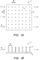
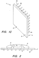
- One conventional heat sink is shown in Figures 1A, 1B and 1C.
- the heat sink 1 includes a base member 2, having a base surface 3 which is attachable to a corresponding surface of the semiconductor package.
- Heat sink 1 is also provided with a heat dissipating surface 5.
- the surface 5 includes pin-fins 4a, 4b, ... 4n which provide greater surface area for convection cooling. Forced convection may be provided by a fan which passes air over a circuit board to which the packaged semiconductor is mounted, or, in some cases, a fan may be mounted directly onto the top of the heat sink pin-fins themselves.
- the encapsulated package shown in cross-section in Figure 2.
- the particular encapsulated package shown is referred to as a ball grid array ("BGA").
- BGA ball grid array
- the semiconductor die 6 is attached to a substrate 7 by a suitable adhesive, or die attach material 8.
- Substrate 7 is typically of laminar construction and various electrically conductive paths are formed on individual layers. Electrical connection between the individual layers is provided by vias in the substrate. Electrical connection between the I/O bond pads on the die 6 and conductive paths provided on the substrate 7 is provided by bond wires 9.
- the conductive paths on substrate 7 are coupled to electrically conductive members, i.e., solder balls 10 which provide electrical connection to a printed circuit board ("PCB").
- PCB printed circuit board
- the chip is encapsulated with, for example, epoxy 11 to form what is sometimes referred to as a "glob-top.”
- Similar encapsulated packages include, for example, pin grid array packages (“PGA”) which provide cylindrical pins in place of the solder balls 10 shown in the figure.
- the substrate 7 is constructed from either a ceramic material, in which case the package is referred to as a ceramic ball grid array (“CBGA”), or a plastic material, in which case the package is referred to as a plastic ball grid array (“PBGA”).
- CBGA ceramic ball grid array
- PBGA plastic ball grid array
- the ceramic substrates offer certain advantages over plastic substrates with respect to heat conductivity, mechanical strength and moisture resistance
- plastic substrates are being increasingly used because of lower manufacturing costs and their ability to provide thinner overall packages.
- advances in manufacturing have improved the plastic substrates relative to their ceramic counterparts. For example, improvements in sealing the laminar layers of the plastic substrates have made them almost as moisture resistant as ceramic substrates.
- a semiconductor package comprises: a semiconductor die mounted to an upper surface of a package substrate, the semiconductor die having a plurality of bond pads which are electrically coupled to conductive traces formed on the package substrate; a plurality of conductive members attached to a lower surface of the package substrate and coupled to conductive traces formed on the package substrate, wherein the conductive members are connectable to conductive traces formed on a printed circuit board to provide electrical connection between the bond pads on the semiconductor die and the conductive traces formed on the printed circuit board; a heat sink comprising: a base member having an upper surface and a lower surface, the lower surface being attachable to a surface of a semiconductor package; and a plurality of heat dissipating pin-fins, wherein each pin-fin of the plurality comprises a bonding point and a distal end, wherein each pin-fin of the plurality is coupled to the upper surface of the base member at the bonding
- a heat sink useful in semiconductor packages.
- a heat sink comprises: a base member having an upper surface and a lower surface, the lower surface being attachable to a surface of a semiconductor package; and a plurality of heat dissipating pin-fins, wherein each pin-fin of the plurality comprises a bonding point and a distal end, wherein each pin-fin of the plurality is coupled to the upper surface of the base member at the bonding point, wherein each pin-fin of the plurality of heat dissipating pin-fins comprises at least one fin.
- Figure 1A is a top view of a conventional pin-fin heat sink.
- Figure 1B is a side view of the conventional pin-fin heat sink shown in Figure 1A.
- Figure 1C is a perspective view of the conventional pin-fin heat sink shown in Figures 1A and 1B.
- Figure 2 is a cross-sectional side view of a ball grid array (“BGA”) semiconductor package.
- BGA ball grid array
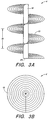
- Figure 3A is a side view of a single pin-fin of the present invention with a spiral fin.
- Figure 3B is a top view of the pin-fin shown in Figure 3A.
- Figure 4 is a side view of a single pin-fin of the present invention with a plurality of disc fins.
- Figure 5 is a top view of an embodiment of the single pin-fin shown in figure 4, this embodiment having circular disc fins.
- Figure 6 is a top view of an embodiment of the single pin-fin shown in figure 4, this embodiment having square disc fins.
- Figure 7 is a side view of a pin-fin with a plurality of disc fins which are warped.
- Figure 8 is a side view of a pin-fin with a plurality of disc fins which are corrugated.
- Figure 9 is a side view of a pin-fin with a plurality of disc fins which are corrugated and placed in an offset fashion.
- Figure 10A is a top view of a heat sink embodiment of the present invention having pin-fins arranged in in-line fashion.
- Figure 10B is a side view of the heat sink embodiment of the present invention having pin-fins shown in Figure 10A.
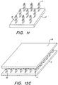
- Figure 11 is a perspective view of a heat sink of the present invention having pin- fins attached thereto with spiral fins.
- Figure 12A is a top view of a heat sink embodiment of the present invention having pin-fins arranged in staggered fashion.
- Figure 12B is a side view of the heat sink embodiment of the present invention having pin-fins shown in Figure 12A.
- Figure 13A is a top view of a ducted heat sink embodiment of the present invention.
- Figure 13B is a side view of the ducted heat sink embodiment shown in Figure 13A.
- Figure 13C is a perspective view of a ducted heat sink embodiment similar to that shown in Figures 13A and 13B, except the pin-fins have spiral fins.
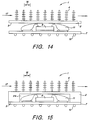
- Figure 14 is a cross-sectional side view of a heat sink of the present invention attached to a semiconductor package.
- Figure 15 is a cross-sectional side view of a heat sink of the present invention having a recess, attached to a semiconductor package.
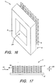
- Figure 16 is a perspective view of a heat sink of the present invention having a recess.
- Figure 17 is a side view of a heat sink of the present invention having disc fins on adjacent pin-fins which are offset to enable closer placement of the pin-fins to each other.
- the pin-fin 4 comprises a central pin 12 which supports a spiral fin 13.
- the central pin 12 has a bonding point 20 for attaching the central pin to a base member of a heat sink.
- the spiral fin 13 is attached to the central pin 12 beginning at the bottom of the central pin 12, circling around the central pin 12 in an upward spiral fashion until it reaches the top of the central pin 12.
- the size of the spiral fin 13 is defined by the radius of the spiral and the pitch 15 of the spiral fin 13.
- the pitch 15 is a measurement of the distance between two consecutive windings of the spiral fin 13 in a direction parallel to the central pin 12.
- an optimum pitch is that which provides the greatest heat dissipation by having a perfect balance between the surface area and the turbulence of the air flow.
- FIG. 4 a side view of an alternative embodiment of the pin-fin is shown.
- the central pin 12 has a bonding point 20 for attaching the central pin 12 to a base member of a heat sink and several disc fins 14 attached thereto.
- the disc, fins 14 are planar and perpendicular to the central pin 12.
- the pitch 15 is a measure of the distance between two adjacent disc fins 14. Of course, the more disc fins 14 attached to the central pin 12, the greater the surface area of the particular pin-fin 4 and the smaller the pitch 15.
- FIG. 5 a top view of an alternative embodiment of the pin-fin shown in Figure 4 is depicted.
- the central pin 12 and disc fins 14 are circular.
- the circular disc fins are more advantageous where it is desirable to have densely packed pin-fins on a heat sink.
- Figure 6 a top view of an embodiment of the pin-fin shown in Figure 4 is shown.
- both the central pin 12 and the disc fins 14 are rectangularly shaped.
- the square comers of the central pin 12 induce turbulence in the fluid which flows around the pin-fin.
- the square disc fins 14 provide additional surface area depending on the proximity and placement of adjacent pin-fins.
- Another center pin 12 has a corrugated, dimpled or bumpy surface to further induce turbulence at the surface of the center pin 12.
- the disc fins 14 and spiral fins 13 also may have a dimpled or bumpy surface to further induce turbulence at the surface of the fins.
- Figure 7 is a side view of a pin-fin having square disc fins 14 attached to a central pin 12.
- the square disc fins 14 have warped comers 19 which are turned up and down.
- the warped corners 19 induce turbulence around the pin-fin 4.
- alternative embodiments comprise spiral and disc fins which are corrugated.
- a side view of one embodiment with corrugated disc fins 14 is shown in Figure 8. While the corrugation shown has a "V" shaped cross-section, other cross- sections are also possible such as a "square block" shape and a sinusoidal shape.
- the heat exchanging fluid passes over the pin-fin 4 from different directions, it is preferred to attach the different disc fins 14 to the central pin 12 with the corrugation lines running in different directions. This ensures that the corrugation lines of at least one disc fin are transverse to the direction of fluid flow.
- the increased turbulence caused by the corrugations results in increased impingement and mixing of the particles that make up the fluid which flows around the pin-fins 4 of the heat sink 1.
- the increased impingement and mixing effectively results in an increase in the heat transfer coefficient.
- an increased heat transfer coefficient results in greater heat transfer Q for a particular heat sink.
- the amount of increased turbulence in the fluid flow can be controlled by adjusting the corrugation angle 21 shown in Figure 8.
- Any suitable corrugation angle can be chosen, from 0, i.e., a planar fin, to 90°.
- the invention comprises a plurality of corrugated disc fins having a corrugation angle a of between about 5° and about 90°.
- the amount of turbulence in the fluid flow through the space between adjacent disc fins 14 of the same pin-fin 4 may also be controlled by offsetting the undulations in one disc fin 14 with those in adjacent disc fin 14.
- the undulations in adjacent disc fins correspond to other.
- adjacent disc fins are disposed such that when an undulation increases in one direction in one disc fin, the corresponding undulation the adjacent disc fin decreases in the same direction.
- the distance between the walls of the disc fins changes along their lengths.
- turbulence of the fluid flow can be increased by providing different corrugation angles to different disc fins attached to the same central pin.
- the pitch 15 is an important factor in determining the surface area of the pin-fin. Because heat is transferred to the pin-fin at the bonding point 20 of the central pin 12 from the base member 2 of the heat sink 1, it is desirable to have as much pin-fin surface area near the base member of the heat sink. Therefore, in an embodiment of the pin-fin 4, the pitch 15 of the pin-fin 4 increases from the bonding point 20 toward the distal end of the pin-fin.
- an embodiment comprises a pin-fin wherein the pitch decreases from the bonding point 20 toward the distal end of the pin-fin.
- FIG. 10A, and 10B top and side views of a heat sink of the present invention are shown.
- the heat sink 1 has a rectangular base member 2 with a plurality of pin-fins 4 which protrude perpendicularly from the base member 2 and placed in in-line fashion.
- the pin-fins 4 are attached to the base member 2 to create a pattern wherein channels 16 are created between the rows of pins in transverse directions.
- a perspective view of a similar embodiment of the invention having spiral pin-fins is shown in Figure 11. These embodiments are preferred where it is desirable to move a large volume of heat exchanging fluid across the heat sink with little resistance.
- heat exchanging fluid which flows along fluid flow lines 17 passes easily between the pin-fins through the channels 16.
- These embodiments are particularly applicable to large heat sinks where uniform heat dissipation is important across the entire surface of the heat sink.
- the pin-fins 4 are either machined or molded and then bonded to the heat sink base member 2 by soldering the pin-fins 4 to the base member 2.
- the pin-fins 4 are constructed from a high thermal conductivity material, such as copper, aluminum or high thermal conductivity plastic, or any other material known to persons of skill.
- FIGS. 12A and 12B top and side views of a heat sink of the present invention are shown.
- Pin-fins 4 are perpendicularly attached to base member 2 according to a particular pattern and placed in staggered fashion.
- the pin-fins 4 are more densely packed to create channels 16 which are neither perpendicular nor parallel to fluid flow lines 17.
- As heat exchanging fluid enters one side of the heat exchanger the fluid passes from side to side as it flows around the pin-fins 4 until it reaches the opposite side of the heat sink 1.
- This pattern significantly increases the turbulence of the heat exchanging fluid.
- the heat sink is effectively a quasi-ducted heat sink.
- planar disc fins of one pin-fin are immediately adjacent the planar disc fins of the next pin-fin.
- Each level of planar disc fins which are equidistant from the base member 2 of the heat sink 1, collectively form a ducting surface which forces heat exchanging fluid to remain close to the base member 2 as it passes over the heat sink.
- a further embodiment of the heat sink has pin-fins 4 with spiral fins 13.
- the spiral fins 13 wrap around the central pins 12 of each pin-fin 4 in clockwise or counterclockwise directions.
- the turbulence may be increased by alternating the direction of wrap of the spiral fins 13 for adjacent pin-fins 4.
- FIGS 13A and 13B depict a heat sink 1 according to still a further embodiment of the invention.
- the heat sink 1 is similar to the heat sink shown in Figures 10A and 10B and has a base member 2 having a lower base surface 3 and an upper-heat dissipating surface 5.
- Pin-fins 4 are attached perpendicularly to the upper heat dissipating surface 5 of the heat sink base 2.
- a top plate 18 is disposed on top of the pin- fins 4 in order to create a ducted heat sink which allows air flow through the space between the base member 2 and the top plate 18.
- the air, or other fluid, which flows through the heat sink 1 must go through the space between the base member 2 and the top plate 18 and cannot rise, or fall, perpendicularly from the heat sink base 2, as is the case in the heat sink shown in Figures 10A and 10B.
- This version of the invention is particularly useful if fluid flow by-pass is undesirable from the top surface of the heat sink.
- a top plate 18 may be used with most all embodiments of the invention.
- Figure 13C shows a perspective view of a ducted heat sink similar to the embodiment shown in Figure 13A and 13B. Rather than disc fins, however, the pin-fins 4 have spiral fins 13.
- the invention is adaptable especially to encapsulated, or "glob-top" packages, such as that shown in Figure 2.
- Figure 14 is a cross-sectional view illustrating one difficulty of attaching a heat sink 1 to a glob top package.
- the base member 2 of the heat sink 1 rests upon the encapsulate 11 of the package. This creates a gap between the lower base surface 3 of the heat sink 1 and the package substrate 7. This gap makes correct fitting of the heat sink 1 to the semiconductor package difficult, and increases mechanical stresses on the package.
- FIG 16 is a perspective view of an embodiment of the invention which overcomes the above problem.
- the heat sink 1 is provided with a plurality of pin-fins, as described above.
- the pin-fins 4 are attached to the upper surface 5 of the heat sink base member 2.
- a recess 24 is formed in the lower base surface 3 of the heat sink base member 2. The dimensions of the recess 24 are such that it receives the encapsulate 11 of the package substrate. This is illustrated in greater detail in Figure 15.
- Figure 15 shows a cross-sectional view of the embodiment of the invention shown in Figure 16 as attached to a glob-top package.
- the recess 24 receives the encapsulate 11 formed on the package substrate 7. This permits the lower base surface 3 of the heat sink base member 2 to rest directly against the substrate 7.
- the heat sink 1 may be attached to the package substrate by conventional methods, such as mechanical clips, or adhesives.
- FIG. 17 a side view of a heat sink of the present invention is shown.
- the heat sink 1 is equipped with pin-fins 4 which are perpendicularly attached to a base member 2 of the heat sink 1.
- Each of the pin-fins 4 has several disc fins 14 attached to each central pin 12 of the pin-fins 4.
- the disc fins 14 of adjacent pin-fins 4 are offset 25 from each other to enable the pin-fins to be more densely packed on the heat sink.
- the disc fins 14 of one pin-fin 4 protrude between or overlap the disc fins 14 of the adjacent pin-fins 4 so that the central pins 12 of each of the pins-fins are spaced more closely to each other than possible without offset, overlapping disc fins.
- a similar embodiment of the invention comprises pin-fins with spiral fins wherein adjacent pin-fins have spiral fins which rotate upwardly in the same direction and have similar pitch. The adjacent spiral fins overlap.
Landscapes
- Cooling Or The Like Of Semiconductors Or Solid State Devices (AREA)
Applications Claiming Priority (2)
| Application Number | Priority Date | Filing Date | Title |
|---|---|---|---|
| US86908097A | 1997-06-04 | 1997-06-04 | |
| US869080 | 1997-06-04 |
Publications (2)
| Publication Number | Publication Date |
|---|---|
| EP0883179A2 true EP0883179A2 (fr) | 1998-12-09 |
| EP0883179A3 EP0883179A3 (fr) | 2000-04-26 |
Family
ID=25352885
Family Applications (1)
| Application Number | Title | Priority Date | Filing Date |
|---|---|---|---|
| EP98109814A Withdrawn EP0883179A3 (fr) | 1997-06-04 | 1998-05-29 | Dissipateur de chaleur à ailettes hélicoidales pour des empaquetages électroniques |
Country Status (2)
| Country | Link |
|---|---|
| EP (1) | EP0883179A3 (fr) |
| JP (1) | JPH1154675A (fr) |
Cited By (9)
| Publication number | Priority date | Publication date | Assignee | Title |
|---|---|---|---|---|
| WO2002056660A3 (fr) * | 2001-01-11 | 2002-08-29 | Satcon Technology Corp | Dispositif d'echange thermique a vis helicoidiale, ensembles de tels dispositifs et procede de fabrication de ces dispositifs |
| US6886627B2 (en) * | 2003-06-27 | 2005-05-03 | Intel Corporation | Radial heat sink with helical shaped fins |
| US20150121701A1 (en) * | 2009-10-03 | 2015-05-07 | Wolverine Tube, Inc. | Cold Plate with Pins |
| CN106358424A (zh) * | 2016-10-18 | 2017-01-25 | 池州脉纬散热器有限责任公司 | 一种含有静态混合器的水冷散热器 |
| US20170023313A1 (en) * | 2015-07-06 | 2017-01-26 | General Electric Company | Thermal management system |
| US10082345B1 (en) | 2014-08-15 | 2018-09-25 | Dometic Sweden Ab | Fin pack cooling assembly |
| CN110174006A (zh) * | 2019-06-20 | 2019-08-27 | 哈尔滨理工大学 | 一种三层螺旋换热管 |
| US20200102839A1 (en) * | 2018-09-28 | 2020-04-02 | United Technologies Corporation | Ribbed pin fins |
| JP2022189543A (ja) * | 2021-06-11 | 2022-12-22 | 株式会社ティラド | 熱交換器用ピンフィンおよび熱交換器 |
Families Citing this family (5)
| Publication number | Priority date | Publication date | Assignee | Title |
|---|---|---|---|---|
| JP2007129183A (ja) * | 2005-10-03 | 2007-05-24 | Sumitomo Electric Ind Ltd | 冷却部材 |
| JP2015164393A (ja) * | 2014-01-28 | 2015-09-10 | 学校法人日本大学 | ヒートシンク及び複合型太陽エネルギー変換装置 |
| USD805019S1 (en) | 2015-05-15 | 2017-12-12 | Dometic Sweden Ab | Accessory base |
| USD805458S1 (en) | 2015-05-15 | 2017-12-19 | Dometic Sweden Ab | Accessory base |
| KR102308872B1 (ko) | 2021-02-02 | 2021-10-05 | 제엠제코(주) | 반도체 부품 쿨링 시스템, 반도체 부품 쿨링 시스템 제조방법, 및 반도체 부품 쿨링 시스템이 적용된 반도체 패키지 |
Family Cites Families (8)
| Publication number | Priority date | Publication date | Assignee | Title |
|---|---|---|---|---|
| EP0054597A1 (fr) * | 1980-12-18 | 1982-06-30 | International Business Machines Corporation | Dispositif pour le refroidissement des broches de modules |
| FR2545274B1 (fr) * | 1983-04-29 | 1985-07-05 | Thomson Csf | Procede de fabrication d'un dissipateur thermique a picots et dissipateur obtenu par ce procede |
| US4546405A (en) * | 1983-05-25 | 1985-10-08 | International Business Machines Corporation | Heat sink for electronic package |
| JPS62213691A (ja) * | 1986-03-14 | 1987-09-19 | Komatsu Ltd | 熱交換フイン |
| JPH0273697A (ja) * | 1988-09-09 | 1990-03-13 | Hitachi Ltd | 放熱フイン |
| JPH0661667A (ja) * | 1992-08-07 | 1994-03-04 | Fujitsu Ltd | 冷却用フィン |
| JPH0669385A (ja) * | 1992-08-21 | 1994-03-11 | Daiyamondo Denki Kk | ヒートシンク |
| JPH06275752A (ja) * | 1993-03-18 | 1994-09-30 | Hitachi Ltd | 半導体装置の冷却装置 |
-
1998
- 1998-05-29 EP EP98109814A patent/EP0883179A3/fr not_active Withdrawn
- 1998-06-04 JP JP10155641A patent/JPH1154675A/ja active Pending
Cited By (11)
| Publication number | Priority date | Publication date | Assignee | Title |
|---|---|---|---|---|
| WO2002056660A3 (fr) * | 2001-01-11 | 2002-08-29 | Satcon Technology Corp | Dispositif d'echange thermique a vis helicoidiale, ensembles de tels dispositifs et procede de fabrication de ces dispositifs |
| US6886627B2 (en) * | 2003-06-27 | 2005-05-03 | Intel Corporation | Radial heat sink with helical shaped fins |
| US20150121701A1 (en) * | 2009-10-03 | 2015-05-07 | Wolverine Tube, Inc. | Cold Plate with Pins |
| US10082345B1 (en) | 2014-08-15 | 2018-09-25 | Dometic Sweden Ab | Fin pack cooling assembly |
| US20170023313A1 (en) * | 2015-07-06 | 2017-01-26 | General Electric Company | Thermal management system |
| US10598443B2 (en) * | 2015-07-06 | 2020-03-24 | General Electric Company | Thermal management system |
| CN106358424A (zh) * | 2016-10-18 | 2017-01-25 | 池州脉纬散热器有限责任公司 | 一种含有静态混合器的水冷散热器 |
| US20200102839A1 (en) * | 2018-09-28 | 2020-04-02 | United Technologies Corporation | Ribbed pin fins |
| US10907480B2 (en) * | 2018-09-28 | 2021-02-02 | Raytheon Technologies Corporation | Ribbed pin fins |
| CN110174006A (zh) * | 2019-06-20 | 2019-08-27 | 哈尔滨理工大学 | 一种三层螺旋换热管 |
| JP2022189543A (ja) * | 2021-06-11 | 2022-12-22 | 株式会社ティラド | 熱交換器用ピンフィンおよび熱交換器 |
Also Published As
| Publication number | Publication date |
|---|---|
| JPH1154675A (ja) | 1999-02-26 |
| EP0883179A3 (fr) | 2000-04-26 |
Similar Documents
| Publication | Publication Date | Title |
|---|---|---|
| US5940271A (en) | Stiffener with integrated heat sink attachment | |
| US6670699B2 (en) | Semiconductor device packaging structure | |
| US6011304A (en) | Stiffener ring attachment with holes and removable snap-in heat sink or heat spreader/lid | |
| US9299634B2 (en) | Method and apparatus for cooling semiconductor device hot blocks and large scale integrated circuit (IC) using integrated interposer for IC packages | |
| KR100963207B1 (ko) | 집적회로 패키지에서 다이들 상의 과열점들에 대한 열적향상 | |
| US7050303B2 (en) | Semiconductor module with vertically mounted semiconductor chip packages | |
| US7772692B2 (en) | Semiconductor device with cooling member | |
| JP2901835B2 (ja) | 半導体装置 | |
| EP0054539B1 (fr) | Dispositif semi-conducteur à circuit intégré comprenant un dissipateur de chaleur | |
| US20060249827A1 (en) | Method and apparatus for forming stacked die and substrate structures for increased packing density | |
| JPH1174431A (ja) | フリップチップ型ヒートシンクを取り付けるための溝を備えた半導体ダイ | |
| US6700783B1 (en) | Three-dimensional stacked heat spreader assembly for electronic package and method for assembling | |
| JPH0677357A (ja) | 改良された半導体パッケージ、集積回路デバイスをパッケージする改良された方法、および半導体デバイスを冷却する方法 | |
| US20160174416A1 (en) | Electronic module with laterally-conducting heat distributor layer | |
| JPH1154675A (ja) | 電子装置パッケージ用ヒートシンク | |
| KR960000222B1 (ko) | 히트-싱크를 갖춘 반도체 패키지 | |
| JP2002184915A (ja) | Lsiの放熱方式 | |
| KR100653605B1 (ko) | 메탈 코어 히트싱크를 구비하는 반도체 칩 패키지와 그를포함하는 반도체 모듈 | |
| WO1997044824A1 (fr) | Boitier haute densite pour puce a circuit integre | |
| US5977622A (en) | Stiffener with slots for clip-on heat sink attachment | |
| JPH02276264A (ja) | ヒートシンク付セラミックパッケージ | |
| US20050157469A1 (en) | Cooling arrangement for a printed circuit board with a heat-dissipating electronic element | |
| JPH04234153A (ja) | ヒートシンク付半導体パッケージ | |
| US20030020160A1 (en) | Semiconductor device die and package having improved heat dissipation capability | |
| JP2961976B2 (ja) | ヒートシンク付半導体パッケージ |
Legal Events
| Date | Code | Title | Description |
|---|---|---|---|
| PUAI | Public reference made under article 153(3) epc to a published international application that has entered the european phase |
Free format text: ORIGINAL CODE: 0009012 |
|
| AK | Designated contracting states |
Kind code of ref document: A2 Designated state(s): AT BE CH CY DE DK ES FI FR GB GR IE IT LI LU MC NL PT SE |
|
| AX | Request for extension of the european patent |
Free format text: AL;LT;LV;MK;RO;SI |
|
| PUAL | Search report despatched |
Free format text: ORIGINAL CODE: 0009013 |
|
| AK | Designated contracting states |
Kind code of ref document: A3 Designated state(s): AT BE CH CY DE DK ES FI FR GB GR IE IT LI LU MC NL PT SE |
|
| AX | Request for extension of the european patent |
Free format text: AL;LT;LV;MK;RO;SI |
|
| AKX | Designation fees paid | ||
| STAA | Information on the status of an ep patent application or granted ep patent |
Free format text: STATUS: THE APPLICATION IS DEEMED TO BE WITHDRAWN |
|
| 18D | Application deemed to be withdrawn |
Effective date: 20000601 |