EP0884602B1 - Pré-amplificateur à faible bruit pour tête de type magnétorésistif - Google Patents
Pré-amplificateur à faible bruit pour tête de type magnétorésistif Download PDFInfo
- Publication number
- EP0884602B1 EP0884602B1 EP98304382A EP98304382A EP0884602B1 EP 0884602 B1 EP0884602 B1 EP 0884602B1 EP 98304382 A EP98304382 A EP 98304382A EP 98304382 A EP98304382 A EP 98304382A EP 0884602 B1 EP0884602 B1 EP 0884602B1
- Authority
- EP
- European Patent Office
- Prior art keywords
- preamplifier
- current
- output
- switching device
- output amplifier
- Prior art date
- Legal status (The legal status is an assumption and is not a legal conclusion. Google has not performed a legal analysis and makes no representation as to the accuracy of the status listed.)
- Expired - Lifetime
Links
Images

Classifications
-
- H—ELECTRICITY
- H03—ELECTRONIC CIRCUITRY
- H03F—AMPLIFIERS
- H03F1/00—Details of amplifiers with only discharge tubes, only semiconductor devices or only unspecified devices as amplifying elements
- H03F1/26—Modifications of amplifiers to reduce influence of noise generated by amplifying elements
-
- G—PHYSICS
- G01—MEASURING; TESTING
- G01R—MEASURING ELECTRIC VARIABLES; MEASURING MAGNETIC VARIABLES
- G01R33/00—Arrangements or instruments for measuring magnetic variables
- G01R33/02—Measuring direction or magnitude of magnetic fields or magnetic flux
- G01R33/06—Measuring direction or magnitude of magnetic fields or magnetic flux using galvano-magnetic devices
- G01R33/09—Magnetoresistive devices
Definitions
- the present invention relates, in general, to the field of preamplifier circuit design. More particularly, the present invention relates to a low noise preamplifier for a magnetoresistive ("MR”) data transducer, or "read” head which reduces the noise contributions of the load resistor in a first stage of the preamplifier in addition to lessening that noise otherwise contributed by the second gain stage of the preamplifier.
- MR magnetoresistive
- Magnetoresistive read heads are known to be useful in reading data encoded on a magnetic surface with a sensitivity exceeding that of inductive or other thin-film heads.
- an MR head is used to detect magnetic field signal changes from a magnetic surface due to the fact that the resistance of the MR sensor changes as a function of the direction and amount of flux being sensed.
- a transverse bias field it must be subjected to a transverse bias field to linearize its response, in addition to a longitudinal bias to minimize Barkhausen noise.
- Various techniques for effectuating such transverse biasing are known, including current shunt biasing and soft adjacent film biasing. The transverse bias field is applied normal to the plane of the magnetic media and parallel to the surface of the MR sensor.
- a low noise preamplifier design which overcomes the disadvantages inherent in prior designs and is configured such that the current through the load resistor may be made much smaller than previous designs. As such, it is possible to achieve a relatively large gain in the first stage of the low noise preamplifier thereby reducing the noise contribution of the load resistor and, concurrently, significantly reducing the noise contribution of the second stage as well.
- a preamplifier which is coupled between first and second supply voltage lines and includes a switching device having first and second current carrying terminals and a control terminal thereof.
- a load resistance couples the first current carrying terminal of the switching device to the first supply voltage line and a variable resistance couples the second current carrying terminal of the switching device to the second supply voltage line.
- An output amplifier has a first input thereof coupled to the first current carrying terminal of the switching device and a second input thereof coupled to a reference voltage.
- the output amplifier presents at least one output providing an output signal of the preamplifier.
- a voltage input/current output amplifier also has first and second inputs thereof coupled to the first and second inputs of the output amplifier respectively, and has an output coupled to the control terminal of the switching device.
- the output of the voltage input/current output amplifier is capacitively coupled to the second supply voltage line.
- a first current source is provided for supplying a first substantially fixed current to the first current carrying terminal of the switching device; and a second current source supplys a second substantially fixed current to the variable resistance.
- the variable resistance comprises an MR read head.
- Also disclosed herein is a method according to independent claim 16 for improving noise immunity in a preamplifier.
- the prior art preamplifier 10 comprises, in pertinent part, first and second amplification stages 12, 14 coupled between a supply voltage source (“V DD ”) and circuit ground (“Gnd”).
- the first stage 12 comprises a load resistor 16 ("R L ”) coupling the collector terminal of a bipolar transistor 18 ("Q 1 ”) to V DD .
- the emitter terminal of transistor 18 is coupled to Gnd through the series connected variable resistance of an MR read head 20 ("R H ").
- the second stage 14 includes a voltage source 22 ("V REF ”) coupled between V DD and the negative ("-") input of a voltage input/current output amplifier 28, defined as node 26, which has its positive ("+”) input coupled to node 24 between resistor 16 and the collector terminal of transistor 18.
- the output of amplifier 28 is coupled to the base terminal of transistor 18 to provide a drive current thereto defined as node 30.
- Node 30 is coupled to Gnd through capacitor 32 as shown.
- Nodes 24 and 26 are coupled to the positive and negative inputs of an additional differential output amplifier 34 respectively which presents corresponding differential outputs 36 ("Out P") and 38 ("Out N") for the prior art preamplifier 10.
- the prior art preamplifier 10 illustrated is a conventional single-ended input, differential output design used as an MR read head 20 output signal amplifier. It incorporates appropriate transverse biasing of the associated MR read head 20 (represented by resistance R H ) into a linear range.
- the current through the MR read head 20 (R H ) is fixed and a function of the resistance of the head itself.
- the current through R H is approximately equal to V REF /R L and it is possible to program this current value by changing V REF in accordance with the value of R H .
- a critical aspect of any preamplifier design is its noise figure, which, in the case of the prior art preamplifier 10, is a function of the value of the load resistor 16 (R L ).
- the output noise due to RL is proportional to: 1/sqrt(R L ). Due to the fact that the total current through the MR read head 20 is applied through R L , it is not possible to increase the value of R L to reduce the output noise without concomitantly increasing the voltage drop across R L to an undesirable level.
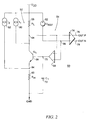
- the preamplifier 50 comprises, in pertinent part, first and second amplification stages 52, 54 coupled between a supply voltage source and circuit ground.
- the first stage 52 comprises a load resistor 56 coupling the collector terminal of a an NPN bipolar transistor 58 to V DD .
- the value of the load resistor 56 may be determined in accordance with the foregoing formula based upon the resistance of the MR read head 60 (R H ) and the transistor 58 may be conveniently furnished as any suitable NPN device.
- the emitter terminal of the transistor 58 is coupled to Gnd through the series connected variable resistance of an MR read head 60.
- the output of amplifier 68 is coupled to the base terminal of transistor 58 to provide a drive current thereto defined as node 70.
- Node 70 is coupled to Gnd through capacitor 72 as shown.
- Nodes 64 and 66 are coupled to the positive and negative inputs of an additional differential amplifier 74 respectively which presents corresponding differential outputs 76 and 78 for the preamplifier 50.
- the capacitor 72 is selected to define the low frequency cut-off of the preamplifier 50 and is a function of g M68 .
- the preamplifier 50 further comprises a first current source 80 ("I 1 ”) coupled between V DD and node 64 in parallel with resistor 56 as well as a second current source 82 (“I 2 ”) coupled between V DD and a node 84 defined by the emitter terminal of transistor 58, which second current source 82 is in parallel with both resistor 56 and series connected transistor 58.
- the relative ratio of the current sourced by the current sources I 1 and I 2 are a function of the resistance of the MR read head 60 (R H ).
- the current through the load resistor 56 may be made much smaller than that in the prior art preamplifier 10 of Fig. 1.
- the first stage 52 comprising resistor 56, transistor 58 and MR read head 60
- the noise contribution of the load resistor 56 R L
- the second stage 54 significantly reducing the noise contribution of the second stage 54 as well.
Landscapes
- Physics & Mathematics (AREA)
- Engineering & Computer Science (AREA)
- Power Engineering (AREA)
- Condensed Matter Physics & Semiconductors (AREA)
- General Physics & Mathematics (AREA)
- Magnetic Heads (AREA)
- Recording Or Reproducing By Magnetic Means (AREA)
- Digital Magnetic Recording (AREA)
- Amplifiers (AREA)
Claims (19)
- Préamplificateur (50) couplé entre des première et seconde lignes de tension d'alimentation, comprenant :caractérisé en ce que le préamplificateur comprend en outre :un dispositif de commutation (58) muni de première et seconde bornes de passage de courant et une borne de commande ;une résistance de charge (56) couplant la première borne de passage de courant du dispositif de commutation à la première ligne de tension d'alimentation (VDD) ;une résistance variable (60) couplant la seconde borne de passage de courant du dispositif de commutation à la seconde ligne de tension d'alimentation (GND) ;un amplificateur de sortie (74) ayant une première entrée couplée à la première borne de passage de courant du dispositif de commutation et une seconde entrée couplée à une tension de référence, l'amplificateur de sortie ayant au moins une sortie fournissant un signal de sortie du préamplificateur ;un amplificateur tension-courant (68) ayant des première et seconde entrées couplées aux première et seconde entrées de l'amplificateur de sortie, respectivement, l'amplificateur tension-courant ayant une sortie couplée à la borne de commande du dispositif de commutation et étant couplée capacitivement à la seconde ligne de tension d'alimentation,une première source de courant (80) pour fournir un premier courant sensiblement fixe à la première borne de passage de courant du dispositif de commutation ; etune seconde source de courant (82) pour fournir un second courant sensiblement fixe à la résistance variable.
- Préamplificateur selon la revendication 1, dans lequel le dispositif de commutation comprend un transistor bipolaire.
- Préamplificateur selon la revendication 2, dans lequel le transistor bipolaire comprend un dispositif NPN.
- Préamplificateur selon la revendication 3, dans lequel les première et seconde bornes de passage de courant et la borne de commande comprennent des bornes de collecteur, d'émetteur et de base, respectivement.
- Préamplificateur selon la revendication 1, dans lequel la résistance de charge comprend une résistance ayant une valeur choisie en fonction de la résistance variable.
- Préamplificateur selon la revendication 1, dans lequel la résistance variable comprend un élément magnéto-résistif.
- Préamplificateur selon la revendication 6, dans lequel l'élément magnéto-résistif comprend une tête de lecture magnéto-résistive.
- Préamplificateur selon la revendication 1, dans lequel l'amplificateur de sortie comprend un amplificateur de tension.
- Préamplificateur selon la revendication 8, dans lequel ladite au moins une sortie de l'amplificateur de sortie comprend deux sorties différentielles (76, 78).
- Préamplificateur selon la revendication 1, dans lequel l'amplificateur tension-courant comprend un amplificateur différentiel.
- Préamplificateur selon la revendication 1, dans lequel la première source de courant fournit un courant choisi en fonction de la résistance variable.
- Préamplificateur selon la revendication 1, dans lequel la seconde source de courant fournit un courant choisi en fonction de la résistance variable.
- Préamplificateur selon la revendication 1, dans lequel la sortie de l'amplificateur tension-courant est couplée capacitivement à la seconde ligne de tension d'alimentation par un condensateur (13) choisi en fonction de la fréquence de coupure du préamplificateur.
- Préamplificateur selon la revendication 1, dans lequel l'amplificateur tension-courant a un gain qui est fonction d'un changement du courant de sortie divisé par un changement de la tension d'entrée du préamplificateur.
- Préamplificateur selon la revendication 1, dans lequel l'amplificateur de sortie a un gain qui est fonction de la résistance de charge divisée par la résistance variable.
- Procédé pour améliorer l'immunité au bruit d'un préamplificateur selon la revendication 1, ce procédé comprenant les étapes suivantes :fourniture d'un premier courant sensiblement fixe à un premier noeud du circuit intermédiaire entre la résistance de charge et le dispositif de commutation, etfourniture également d'un second courant sensiblement fixe à un second noeud du circuit intermédiaire entre le dispositif de commutation et la résistance variable.
- Procédé selon la revendication 16, dans lequel les étapes de fourniture des premier et second courants sont effectuées de sorte que les premier et second courants relativement fixes ont un niveau qui est fonction de la résistance de l'élément de résistance variable.
- Procédé selon la revendication 16, dans lequel l'étape de fourniture de courant est effectuée par une première source de courant.
- Procédé selon la revendication 16, dans lequel l'étape de fourniture de courant est effectuée par une seconde source de courant.
Applications Claiming Priority (2)
| Application Number | Priority Date | Filing Date | Title |
|---|---|---|---|
| US08/872,841 US5939940A (en) | 1997-06-11 | 1997-06-11 | Low noise preamplifier for a magnetoresistive data transducer |
| US872841 | 1997-06-11 |
Publications (2)
| Publication Number | Publication Date |
|---|---|
| EP0884602A1 EP0884602A1 (fr) | 1998-12-16 |
| EP0884602B1 true EP0884602B1 (fr) | 2004-07-14 |
Family
ID=25360407
Family Applications (1)
| Application Number | Title | Priority Date | Filing Date |
|---|---|---|---|
| EP98304382A Expired - Lifetime EP0884602B1 (fr) | 1997-06-11 | 1998-06-03 | Pré-amplificateur à faible bruit pour tête de type magnétorésistif |
Country Status (4)
| Country | Link |
|---|---|
| US (1) | US5939940A (fr) |
| EP (1) | EP0884602B1 (fr) |
| JP (1) | JPH1166505A (fr) |
| DE (1) | DE69824992D1 (fr) |
Families Citing this family (7)
| Publication number | Priority date | Publication date | Assignee | Title |
|---|---|---|---|---|
| US6226141B1 (en) * | 1997-09-19 | 2001-05-01 | Texas Instruments Incorporated | Damp circuit for a hard disk drive write head |
| US6268774B1 (en) | 1999-11-05 | 2001-07-31 | Intel Corporation | Self-tuning amplifier |
| US6798597B1 (en) | 2001-02-02 | 2004-09-28 | Marvell International Ltd. | Write channel having preamplifier and non-uniform transmission line |
| JP4006251B2 (ja) * | 2002-03-20 | 2007-11-14 | キヤノン株式会社 | ミラー装置、ミラーの調整方法、露光装置、露光方法及び半導体デバイスの製造方法 |
| US7187513B2 (en) * | 2002-06-14 | 2007-03-06 | Renesas Technology America, Inc. | Differential magneto-resistive head pre-amplifiers for single polarity power supply applications |
| US6972916B1 (en) | 2003-03-17 | 2005-12-06 | Marvell International Ltd. | Preamplifier arranged in proximity of disk drive head |
| JP2014107730A (ja) * | 2012-11-28 | 2014-06-09 | Yamaha Corp | 信号処理装置および増幅器 |
Family Cites Families (4)
| Publication number | Priority date | Publication date | Assignee | Title |
|---|---|---|---|---|
| JPS55107307A (en) * | 1979-02-08 | 1980-08-18 | Pioneer Electronic Corp | Transistor circuit |
| JPS5742208A (en) * | 1980-08-28 | 1982-03-09 | Sutatsukusu Kogyo Kk | Amplifying circuit for direct coupling circuit |
| JPS589407A (ja) * | 1981-07-08 | 1983-01-19 | Shinshirasuna Denki Kk | 電力増幅回路の特性を改善するための装置 |
| JPH06139525A (ja) * | 1992-10-27 | 1994-05-20 | Sony Corp | 磁気抵抗効果型ヘッド用再生装置 |
-
1997
- 1997-06-11 US US08/872,841 patent/US5939940A/en not_active Expired - Lifetime
-
1998
- 1998-06-03 DE DE69824992T patent/DE69824992D1/de not_active Expired - Lifetime
- 1998-06-03 EP EP98304382A patent/EP0884602B1/fr not_active Expired - Lifetime
- 1998-06-11 JP JP10163807A patent/JPH1166505A/ja active Pending
Also Published As
| Publication number | Publication date |
|---|---|
| EP0884602A1 (fr) | 1998-12-16 |
| DE69824992D1 (de) | 2004-08-19 |
| JPH1166505A (ja) | 1999-03-09 |
| US5939940A (en) | 1999-08-17 |
Similar Documents
| Publication | Publication Date | Title |
|---|---|---|
| EP0586062B1 (fr) | Amplificateur pour un capteur magnétorésistif | |
| US6134060A (en) | Current bias, current sense for magneto-resistive preamplifier, preamplifying integrated circuit, and related methods | |
| JP2572528B2 (ja) | データ記憶装置 | |
| EP0478298A2 (fr) | Pré-amplificateur à faible bruit pour têtes de type magnétorésistif | |
| JPS62245503A (ja) | 磁気記録検出回路 | |
| US6822817B2 (en) | Preamplifier circuit suitable for use in magnetic storage devices | |
| EP0053343A1 (fr) | Circuit de reproduction et d'amplification pour tête magnéto-résistive | |
| US10944366B2 (en) | Advanced load current monitoring circuit and method for a class-AB amplifier | |
| US6341046B1 (en) | Current biasing voltage sensing preamplifier for magnetoresistive heads | |
| US6054901A (en) | Low noise preamplifier | |
| US5345346A (en) | Positive feedback low input capacitance differential amplifier | |
| US5691663A (en) | Single-ended supply preamplifier with high power supply rejection ratio | |
| US5939940A (en) | Low noise preamplifier for a magnetoresistive data transducer | |
| US5155449A (en) | FET buffer amplifier | |
| US6721117B2 (en) | Read/write system with reduced write-to-read transition recovery time independent from input voltage and input current offset | |
| US6909569B2 (en) | Low impedance semiconductor integrated circuit | |
| US5886568A (en) | Open-loop MR biasing circuit with high power supply and common mode rejection | |
| US6222415B1 (en) | Magneto-resistive element signal amplifying circuit | |
| JPH06243405A (ja) | 磁気抵抗素子用プリアンプ | |
| US5717536A (en) | Single-ended cascode amplifier for magnetoresistive sensors | |
| US6211736B1 (en) | Signal amplifying circuit for magnetoresistive element | |
| US6154333A (en) | Amplification circuit | |
| US6208482B1 (en) | Signal amplifying circuit for an MR element | |
| US5694083A (en) | Single end input high frequency amplifier | |
| JP3844544B2 (ja) | 光受信回路 |
Legal Events
| Date | Code | Title | Description |
|---|---|---|---|
| PUAI | Public reference made under article 153(3) epc to a published international application that has entered the european phase |
Free format text: ORIGINAL CODE: 0009012 |
|
| AK | Designated contracting states |
Kind code of ref document: A1 Designated state(s): DE FR GB IT |
|
| AX | Request for extension of the european patent |
Free format text: AL;LT;LV;MK;RO;SI |
|
| RAP3 | Party data changed (applicant data changed or rights of an application transferred) |
Owner name: STMICROELECTRONICS, INC. |
|
| 17P | Request for examination filed |
Effective date: 19990607 |
|
| AKX | Designation fees paid |
Free format text: DE FR GB IT |
|
| GRAP | Despatch of communication of intention to grant a patent |
Free format text: ORIGINAL CODE: EPIDOSNIGR1 |
|
| GRAS | Grant fee paid |
Free format text: ORIGINAL CODE: EPIDOSNIGR3 |
|
| GRAA | (expected) grant |
Free format text: ORIGINAL CODE: 0009210 |
|
| AK | Designated contracting states |
Kind code of ref document: B1 Designated state(s): DE FR GB IT |
|
| PG25 | Lapsed in a contracting state [announced via postgrant information from national office to epo] |
Ref country code: IT Free format text: LAPSE BECAUSE OF FAILURE TO SUBMIT A TRANSLATION OF THE DESCRIPTION OR TO PAY THE FEE WITHIN THE PRESCRIBED TIME-LIMIT;WARNING: LAPSES OF ITALIAN PATENTS WITH EFFECTIVE DATE BEFORE 2007 MAY HAVE OCCURRED AT ANY TIME BEFORE 2007. THE CORRECT EFFECTIVE DATE MAY BE DIFFERENT FROM THE ONE RECORDED. Effective date: 20040714 |
|
| REG | Reference to a national code |
Ref country code: GB Ref legal event code: FG4D |
|
| REF | Corresponds to: |
Ref document number: 69824992 Country of ref document: DE Date of ref document: 20040819 Kind code of ref document: P |
|
| PG25 | Lapsed in a contracting state [announced via postgrant information from national office to epo] |
Ref country code: DE Free format text: LAPSE BECAUSE OF FAILURE TO SUBMIT A TRANSLATION OF THE DESCRIPTION OR TO PAY THE FEE WITHIN THE PRESCRIBED TIME-LIMIT Effective date: 20041015 |
|
| ET | Fr: translation filed | ||
| PLBE | No opposition filed within time limit |
Free format text: ORIGINAL CODE: 0009261 |
|
| STAA | Information on the status of an ep patent application or granted ep patent |
Free format text: STATUS: NO OPPOSITION FILED WITHIN TIME LIMIT |
|
| 26N | No opposition filed |
Effective date: 20050415 |
|
| PGFP | Annual fee paid to national office [announced via postgrant information from national office to epo] |
Ref country code: FR Payment date: 20080617 Year of fee payment: 11 |
|
| PGFP | Annual fee paid to national office [announced via postgrant information from national office to epo] |
Ref country code: GB Payment date: 20080604 Year of fee payment: 11 |
|
| GBPC | Gb: european patent ceased through non-payment of renewal fee |
Effective date: 20090603 |
|
| REG | Reference to a national code |
Ref country code: FR Ref legal event code: ST Effective date: 20100226 |
|
| PG25 | Lapsed in a contracting state [announced via postgrant information from national office to epo] |
Ref country code: FR Free format text: LAPSE BECAUSE OF NON-PAYMENT OF DUE FEES Effective date: 20090630 |
|
| PG25 | Lapsed in a contracting state [announced via postgrant information from national office to epo] |
Ref country code: GB Free format text: LAPSE BECAUSE OF NON-PAYMENT OF DUE FEES Effective date: 20090603 |