EP0884782A1 - Boítier électro-optique intégré et son procédé de fabrication - Google Patents
Boítier électro-optique intégré et son procédé de fabrication Download PDFInfo
- Publication number
- EP0884782A1 EP0884782A1 EP97109441A EP97109441A EP0884782A1 EP 0884782 A1 EP0884782 A1 EP 0884782A1 EP 97109441 A EP97109441 A EP 97109441A EP 97109441 A EP97109441 A EP 97109441A EP 0884782 A1 EP0884782 A1 EP 0884782A1
- Authority
- EP
- European Patent Office
- Prior art keywords
- optical package
- integrated electro
- circuit board
- printed circuit
- layer
- Prior art date
- Legal status (The legal status is an assumption and is not a legal conclusion. Google has not performed a legal analysis and makes no representation as to the accuracy of the status listed.)
- Withdrawn
Links
Images
Classifications
-
- H—ELECTRICITY
- H10—SEMICONDUCTOR DEVICES; ELECTRIC SOLID-STATE DEVICES NOT OTHERWISE PROVIDED FOR
- H10W—GENERIC PACKAGES, INTERCONNECTIONS, CONNECTORS OR OTHER CONSTRUCTIONAL DETAILS OF DEVICES COVERED BY CLASS H10
- H10W90/00—Package configurations
-
- H—ELECTRICITY
- H10—SEMICONDUCTOR DEVICES; ELECTRIC SOLID-STATE DEVICES NOT OTHERWISE PROVIDED FOR
- H10K—ORGANIC ELECTRIC SOLID-STATE DEVICES
- H10K59/00—Integrated devices, or assemblies of multiple devices, comprising at least one organic light-emitting element covered by group H10K50/00
- H10K59/10—OLED displays
- H10K59/17—Passive-matrix OLED displays
- H10K59/179—Interconnections, e.g. wiring lines or terminals
-
- H—ELECTRICITY
- H10—SEMICONDUCTOR DEVICES; ELECTRIC SOLID-STATE DEVICES NOT OTHERWISE PROVIDED FOR
- H10K—ORGANIC ELECTRIC SOLID-STATE DEVICES
- H10K59/00—Integrated devices, or assemblies of multiple devices, comprising at least one organic light-emitting element covered by group H10K50/00
- H10K59/80—Constructional details
- H10K59/87—Passivation; Containers; Encapsulations
- H10K59/871—Self-supporting sealing arrangements
- H10K59/8721—Metallic sealing arrangements
-
- H—ELECTRICITY
- H10—SEMICONDUCTOR DEVICES; ELECTRIC SOLID-STATE DEVICES NOT OTHERWISE PROVIDED FOR
- H10K—ORGANIC ELECTRIC SOLID-STATE DEVICES
- H10K59/00—Integrated devices, or assemblies of multiple devices, comprising at least one organic light-emitting element covered by group H10K50/00
- H10K59/80—Constructional details
- H10K59/87—Passivation; Containers; Encapsulations
- H10K59/871—Self-supporting sealing arrangements
- H10K59/8722—Peripheral sealing arrangements, e.g. adhesives, sealants
-
- H—ELECTRICITY
- H10—SEMICONDUCTOR DEVICES; ELECTRIC SOLID-STATE DEVICES NOT OTHERWISE PROVIDED FOR
- H10W—GENERIC PACKAGES, INTERCONNECTIONS, CONNECTORS OR OTHER CONSTRUCTIONAL DETAILS OF DEVICES COVERED BY CLASS H10
- H10W90/00—Package configurations
- H10W90/701—Package configurations characterised by the relative positions of pads or connectors relative to package parts
- H10W90/721—Package configurations characterised by the relative positions of pads or connectors relative to package parts of bump connectors
- H10W90/724—Package configurations characterised by the relative positions of pads or connectors relative to package parts of bump connectors between a chip and a stacked insulating package substrate, interposer or RDL
Definitions
- the present invention pertains to integrated electro-optical packages and more specifically to integrated electro-optical packages incorporating organic devices.
- a two-dimensional organic LED array for image manifestation apparatus applications is composed of a plurality of organic LEDs (one or more of which form a pixel) arranged in rows and columns.
- Each individual organic LED in the array is generally constructed with a light transmissive first electrode, an organic electroluminescent medium deposited on the first electrode, and a metallic electrode on top of the organic electroluminescent medium.
- the electrodes of the LEDs are connected to form a two-dimensional X-Y addressing pattern.
- the X-Y addressing pattern is achieved by patterning the light transmissive electrodes in an X direction and patterning the metallic electrodes in a Y direction (or vice versa if desired), with the X and Y directions being perpendicular to each other.
- the patterning of the electrodes is usually accomplished by either shadow mask or etching techniques. Due to the technical limits of shadow masks, etching processes are generally being utilized for high density information displays, which have pixel pitches less then 0.1 mm.
- This type of interconnection generally uses flexible cables extending from electrode lines located about an exterior edge of the substrate to a standard printed circuit board. Due to this edge connection, the display module foot print is rather large and only allows, at most, for a dual scan driving scheme. To achieve a higher contrast ratio with passive drivers, multiscan driving schemes are needed.
- electroluminescent organic devices utilize a layer of low work function metal in the cathode to ensure efficient electron injecting electrodes and low operating voltages.
- the low work function metals are reactive and susceptible to oxygen and moisture, and oxidation of the metal limits the lifetime of the devices.
- a hermetic or pseudo-hermetic seal is normally required to achieve long term stability and longevity.
- Several types of hermetic seals are utilized, the most common of which are inorganic materials, such as metals and the like.
- a problem that occurs in the fabrication and passivation of electroluminescent organic devices is a result of the fact that the organic layers of the electroluminescent organic devices can not withstand very high temperatures (i.e. generally greater than approximately 300° C). In many instances, even approaching the critical temperatures of the organic layers, especially if the elevated temperatures are maintained for relatively long periods of time, can degrade the materials used and reduce the reliability and/or the longevity of the resulting devices.
- metal cans are very expensive to fabricate and require extensive labor to assemble. Further, metal cans are large and heavy so that they severely limit the applications of electroluminescent organic devices by increasing the thickness and size of the device itself.
- a more recent means of hermetically sealing electroluminescent organic devices is to overcoat them with an inorganic material, such as a dielectric or metal, to achieve a hermetic seal.
- an inorganic material such as a dielectric or metal
- the electroluminescent organic devices are very susceptible to the high temperatures normally required during deposition of dielectrics and metals.
- the ceramic or metal material generally must be deposited by PECVD methods in order to meet the low temperature criteria.
- the major problem with this method of sealing is that during the PECVD deposition there is a strong possibility of radiation damage to the electroluminescent organic device.
- an integrated electro-optical package or light emitting device display module, that includes a plurality of organic light emitting devices (LEDs) directly interconnected to external driver circuits utilizing a printed circuit board, having formed therein a plurality of plated through-hole vias and a method of fabricating the integrated electro-optical package.
- LEDs organic light emitting devices
- the organic LEDs of the present invention are fabricated on a supporting substrate that includes a plurality of parallel, laterally spaced apart, optically transparent, electrically conductive strips positioned on a surface of the supporting substrate so as to define a plurality of first electrodes.
- Electroluminescent media are positioned on each of the plurality of first electrodes so as to define a light emitting diode in conjunction with an associated first electrode of each of the plurality of electrodes.
- a layer of metal is positioned over the electroluminescent medium so as to define a plurality of parallel, laterally spaced apart, metallic strips orthogonal to the plurality of transparent conductive strips. The laterally spaced apart, metallic strips define a second electrode for each of the light emitting diodes.
- Each electrically conductive strip of the plurality of electrically conductive strips, forming the plurality of first electrodes, and each metallic strip of the plurality of metallic strips, forming the plurality of second electrodes has an end in electrical contact with a plated through-hole conductive via and conductive leads, formed in a multi-layer printed circuit board, electrically interfaced utilizing conductive epoxy.
- a hermetic seal is formed by positioning a sealing ring formed on the printed circuit board in sealing contact with a sealing area on the surface of the substrate of the organic device so as to hermetically seal the organic light emitting devices utilizing a sealant material, such as an epoxy adhesive.
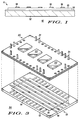
- FIG. 1 is a simplified cross-sectional view of a partial array 11 of an organic light emitting device 10 according to the present invention.
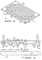
- FIG. 2 is a perspective view of a supporting substrate having formed thereon the array 11 of light emitting devices, thereby forming the light emitting device 10 of the integrated electro-optical package of the present invention.
- substrate 12 of the organic light emitting device 10, as seen along line 1-1 of FIG. 2, portions being broken away so that only a portion of substrate 12 can be seen.
- Substrate 12 in this specific embodiment, is some optically clear material, such as glass, quartz, a transparent semiconductor material or the like, etc.
- the array 11 of pixels of organic light emitting devices (LEDs) is positioned on substrate 12, generally by fabricating array 11 directly on substrate 12 in any of the various methods of fabricating electroluminescent organic LEDs.
- array 11 includes a transparent layer of conductive material, such as indium-tin-oxide (ITO) or the like, with an active organic media, such as an organic electroluminescent media, positioned thereon and a cathode formed of a metal layer including a thin layer of a low work function metal, thereby defining a plurality of patterned electrodes (discussed presently).
- ITO indium-tin-oxide
- active organic media such as an organic electroluminescent media
- a plurality of parallel, laterally spaced apart, optically transparent, electrically conductive strips 14 are formed on the surface of substrate 12.
- strips 14 are formed by depositing a layer of material and etching the layer to form strips 14 or by masking and performing metal lift-off techniques well known in the art.
- substrate 12 is made of glass or polymeric materials and has deposited thereon a layer of light transmissive, electrically conductive material, which is selected from a variety of organic or inorganic conductors, such as conductive polyaniline (PANI), or indium-tin-oxide (ITO).
- PANI conductive polyaniline
- ITO indium-tin-oxide
- a continuous layer or organic material On the top of conductive strips 14 is deposited a continuous layer or organic material, more specifically a layer of organic electroluminescent medium 15, which generally consists of a layer of hole transporting material, a layer of active emitter material, and a layer of electron transporting material.
- a layer of organic electroluminescent medium 15 which generally consists of a layer of hole transporting material, a layer of active emitter material, and a layer of electron transporting material.
- a layer of low work function metal or a metal alloy On top of the layer of electroluminescent medium 15 is deposited a layer of low work function metal or a metal alloy, capped with a thick layer of stable metal such as aluminum, silver, copper or gold.
- the layer of stable metal is selected to form a good electrical contact with the layer of low work function metal, thereby forming the cathode electrode for LED array 11, more specifically a plurality of metallized strips 16.
- the patterning of the cathode of electrodes, or metallized strips 16, is achieved by either shadow mask techniques or a shadow wall techniques, generally known by those skilled in the art.
- any metals with a work function less than approximately 4.0 eV can be used as the cathode material, e.g. lithium, magnesium, indium, calcium, etc.
- the materials used in the layer of organic electroluminescent medium 15 in the two-dimensional array 11 of this invention can include any of the materials of organic EL devices disclosed in the prior art.
- the layer of organic electroluminescent medium 15 generally consists of a layer of hole transporting material, a layer of active emitter material, and a layer of electron transporting material.
- Polymers, organic molecules and organometallic complexes can be used as hole transporting materials, active emitters and electron transporting materials.
- fluorescent dopants used for enhancement of the device efficiency, as well as achievement of different colors, can also be incorporated.
- the layer of organic electroluminescent medium 15 can be deposited by vacuum evaporation.
- the layer of organic electroluminescent medium 15 can also be deposited by other techniques such as injection-fill, spin-coating, roll-coating, dip-coating or doctor-blading from a suitable solution when polymeric materials are used.
- a mixture of the above-mentioned techniques may be needed in cases where a heterostructure array composed of both small organic molecule materials and polymers is to be built.
- each LED forms a pixel and by addressing specific LEDs by row and column in a well known manner, the specific LEDs are energized to produce an image which is transmitted downwardly through substrate 12.
- LED array 11 and substrate 12 are greatly enlarged in the FIGS.
- the actual size of substrate 12 is on the order of a few milli-meters (2mm to 10mm) along each side with each LED being on the order of 5 to 50 microns on a side (or in diameter if the LED is round)
- conductive strips 14 and metallized strips 16 have a very small cross-section, which severely limits their current carrying capacity, or current density.
- the image is formed by sequentially turning on the rows of pixels and supplying video data to the columns.
- this scheme only one row at a time is addressed or "turned ON".
- the conductive strips 14 for each row need to carry only sufficient current for one LED (the one LED in the row which is ON).
- all of the LEDs in the ON row could potentially be turned ON simultaneously.
- the metallized strips 16 for the ON row which can potentially be required to carry current for however many LEDs are in the row (e.g. 100 to 1500 LEDs), must carry many times as much current as the column metal traces.
- conductive strips 14 will be less conductive than, for example, metallized strips 16. This is because the material must be not only electrically conductive but it must be optically transmissive, or substantially transparent (conduct at least 80% of the light generated in array 11). To offset this difference in conduction, conductive strips 14 are used as column conductors and metallized strips 16 are used as row conductors.
- integrated electro-optical package 30 is composed of two primary components, organic light emitting device 10 and a multi-layer printed circuit board (PCB) 20 having formed thereon driver electronics.
- Multilayer printed circuit board 20 is fabricated according to techniques well known to those skilled in the art, and in general is composed of sandwiched layers of standard FR4 board and circuit routing layers.
- a plurality of driver and control circuits 22 generally are formed as semiconductor chips and are wire bonded or bump bonded to electrical contacts on the upper major surface 21 of PCB 20.
- driver and control circuits 22 making up the driver electronics can be mounted on PCB 20 at any convenient time subsequent to the formation of PCB 20.
- electrically conductive strips 14 and metallized strips 16 of light emitting device 10 are connected to the plurality of row and column drivers and control circuits 22 through a plurality of vertical interconnections 23, utilizing electrical leads, or traces, 25, plated through-hole vias 24 formed in PCB 20, and conductive epoxy 26.
- conductive epoxy 26 can be formed as bumps (as illustrated in FIG.
- a sealing ring 28 of dielectric material is formed on a lower surface of PCB 20.
- a hermetic seal is formed between PCB 20 and light emitting device 10 by using a sealant material 29 to attach sealing ring 28 to a sealant area formed about the perimeter of light emitting device 10. Sealing epoxy, or the like, is used as sealant material 29.
- PCB 20 serves to encapsulate the array 11 of organic light emitting devices and no further encapsulation element, such as a metal can, etc., is required. This utilization of PCB 20, as the encapsulating element, results in a compact organic integrated electro-optical package 30 that is easier to manufacture than prior art methods and devices.
- an improved integrated electro-optical package, or light emitting device display module which is hermetically sealed and incorporates organic type LEDs as the light source.
- improved interconnects and package structures capable of multiscan driving schemes to produce higher contrast ratios utilizing organic LEDs.
- This improved package structure and fabrication techniques substantially reduces the limitation on size of the packages in that vertical interconnects are achieved through a printed circuit board which also serves as an encapsulation element.
- the array of LEDs is hermetically sealed from ambient moisture and the environment and there is little or no damage to the organic LEDs, thus greatly improving reliability, as well as being small and compact.
Landscapes
- Electroluminescent Light Sources (AREA)
- Devices For Indicating Variable Information By Combining Individual Elements (AREA)
- Led Devices (AREA)
Priority Applications (5)
| Application Number | Priority Date | Filing Date | Title |
|---|---|---|---|
| US08/660,829 US5703394A (en) | 1996-06-10 | 1996-06-10 | Integrated electro-optical package |
| JP16497997A JP4077905B2 (ja) | 1996-06-10 | 1997-06-05 | 一体型電気光学パッケージおよび作製方法 |
| CN97105461A CN1167966A (zh) | 1996-06-10 | 1997-06-06 | 集成电光组件及制造方法 |
| EP97109441A EP0884782A1 (fr) | 1996-06-10 | 1997-06-11 | Boítier électro-optique intégré et son procédé de fabrication |
| US08/889,724 US5747363A (en) | 1996-06-10 | 1997-07-08 | Method of manufacturing an integrated electro-optical package |
Applications Claiming Priority (2)
| Application Number | Priority Date | Filing Date | Title |
|---|---|---|---|
| US08/660,829 US5703394A (en) | 1996-06-10 | 1996-06-10 | Integrated electro-optical package |
| EP97109441A EP0884782A1 (fr) | 1996-06-10 | 1997-06-11 | Boítier électro-optique intégré et son procédé de fabrication |
Publications (1)
| Publication Number | Publication Date |
|---|---|
| EP0884782A1 true EP0884782A1 (fr) | 1998-12-16 |
Family
ID=26145530
Family Applications (1)
| Application Number | Title | Priority Date | Filing Date |
|---|---|---|---|
| EP97109441A Withdrawn EP0884782A1 (fr) | 1996-06-10 | 1997-06-11 | Boítier électro-optique intégré et son procédé de fabrication |
Country Status (4)
| Country | Link |
|---|---|
| US (2) | US5703394A (fr) |
| EP (1) | EP0884782A1 (fr) |
| JP (1) | JP4077905B2 (fr) |
| CN (1) | CN1167966A (fr) |
Cited By (11)
| Publication number | Priority date | Publication date | Assignee | Title |
|---|---|---|---|---|
| EP1094355A1 (fr) * | 1999-10-19 | 2001-04-25 | Corning Incorporated | Interconnexion electrique de circuits planaires à ondes lumineuses |
| WO2003034513A1 (fr) * | 2001-10-18 | 2003-04-24 | Koninklijke Philips Electronics N.V. | Dispositif electroluminescent |
| US6818464B2 (en) | 2001-10-17 | 2004-11-16 | Hymite A/S | Double-sided etching technique for providing a semiconductor structure with through-holes, and a feed-through metalization process for sealing the through-holes |
| EP1109224A3 (fr) * | 1999-12-15 | 2006-02-01 | Sel Semiconductor Energy Laboratory Co., Ltd. | Dispositif émetteur de lumiére |
| EP1684366A1 (fr) * | 2005-01-25 | 2006-07-26 | Nederlandse Organisatie voor toegepast-natuurwetenschappelijk Onderzoek TNO | Dispositif électronique comprenant un dispositif électronique et un dispositif encapsulant |
| EP1332487A4 (fr) * | 2000-11-10 | 2006-09-06 | Transpacific Ip Ltd | Structure d'affichage a paves mettant en oeuvre des materiaux organiques luminescents |
| US7592970B2 (en) | 1998-02-17 | 2009-09-22 | Dennis Lee Matthies | Tiled electronic display structure |
| US7595588B2 (en) | 2001-03-22 | 2009-09-29 | Microemissive Displays Limited | Electroluminescent device and method of making same |
| US7681306B2 (en) | 2004-04-28 | 2010-03-23 | Hymite A/S | Method of forming an assembly to house one or more micro components |
| DE102011055233A1 (de) * | 2011-11-10 | 2013-05-16 | Novaled Ag | Lichtemittierende Vorrichtung und flächige Anordnung mit mehreren lichtemittierenden Vorrichtungen |
| CN107093615A (zh) * | 2017-04-26 | 2017-08-25 | 上海小糸车灯有限公司 | 一种多片矩阵式oled屏体间的电极连接结构 |
Families Citing this family (82)
| Publication number | Priority date | Publication date | Assignee | Title |
|---|---|---|---|---|
| JP3290584B2 (ja) * | 1996-02-07 | 2002-06-10 | パイオニア株式会社 | 有機エレクトロルミネセンス素子 |
| US5833903A (en) | 1996-12-10 | 1998-11-10 | Great American Gumball Corporation | Injection molding encapsulation for an electronic device directly onto a substrate |
| GB2329756A (en) * | 1997-09-25 | 1999-03-31 | Univ Bristol | Assemblies of light emitting diodes |
| US6057600A (en) * | 1997-11-27 | 2000-05-02 | Kyocera Corporation | Structure for mounting a high-frequency package |
| US6200134B1 (en) * | 1998-01-20 | 2001-03-13 | Kerr Corporation | Apparatus and method for curing materials with radiation |
| DE69937485T2 (de) * | 1998-01-28 | 2008-08-21 | Thin Film Electronics Asa | Methode zur herstellung zwei- oder dreidimensionaler elektrisch leitender oder halbleitender strukturen, eine löschmethode derselben und ein generator/modulator eines elektrischen feldes zum gebrauch in der herstellungsmethode |
| US6370019B1 (en) * | 1998-02-17 | 2002-04-09 | Sarnoff Corporation | Sealing of large area display structures |
| US6476783B2 (en) * | 1998-02-17 | 2002-11-05 | Sarnoff Corporation | Contrast enhancement for an electronic display device by using a black matrix and lens array on outer surface of display |
| US6380563B2 (en) | 1998-03-30 | 2002-04-30 | Micron Technology, Inc. | Opto-electric mounting apparatus |
| US6713788B2 (en) | 1998-03-30 | 2004-03-30 | Micron Technology, Inc. | Opto-electric mounting apparatus |
| JP4189610B2 (ja) * | 1998-05-08 | 2008-12-03 | ソニー株式会社 | 光電変換素子およびその製造方法 |
| WO2000015009A1 (fr) * | 1998-09-02 | 2000-03-16 | Seiko Epson Corporation | Source lumineuse et dispositif d'affichage |
| DE19855828A1 (de) * | 1998-12-03 | 2000-06-08 | Heidenhain Gmbh Dr Johannes | Dreidimensionales Meßmodul |
| JP4273551B2 (ja) * | 1999-01-14 | 2009-06-03 | ソニー株式会社 | 映像装置及びその製造方法 |
| JP4066547B2 (ja) * | 1999-01-25 | 2008-03-26 | 松下電器産業株式会社 | 表示装置 |
| US6274978B1 (en) * | 1999-02-23 | 2001-08-14 | Sarnoff Corporation | Fiber-based flat panel display |
| US6301401B1 (en) | 1999-04-02 | 2001-10-09 | Convergence Technologies, Ltd. | Electro-optical package for reducing parasitic effects |
| GB9911789D0 (en) * | 1999-05-20 | 1999-07-21 | Cambridge Consultants | Electroluminescent devices |
| EP1076357A1 (fr) * | 1999-08-11 | 2001-02-14 | SiMoTec GmbH | Dispositif de montage pour le traitement de microsystèmes |
| DE19943149A1 (de) | 1999-09-09 | 2001-04-05 | Siemens Ag | Verfahren zur Verkapselung von Bauelementen |
| US6515417B1 (en) * | 2000-01-27 | 2003-02-04 | General Electric Company | Organic light emitting device and method for mounting |
| US6559594B2 (en) * | 2000-02-03 | 2003-05-06 | Semiconductor Energy Laboratory Co., Ltd. | Light-emitting device |
| US6608283B2 (en) * | 2000-02-08 | 2003-08-19 | Emagin Corporation | Apparatus and method for solder-sealing an active matrix organic light emitting diode |
| US6590283B1 (en) * | 2000-02-28 | 2003-07-08 | Agere Systems Inc. | Method for hermetic leadless device interconnect using a submount |
| US7320593B2 (en) | 2000-03-08 | 2008-01-22 | Tir Systems Ltd. | Light emitting diode light source for curing dental composites |
| ITPN20000043A1 (it) * | 2000-07-18 | 2002-01-18 | Sapa Autoplastics S P A | Supporto per dispositivi di illuminazione della targa di autoveicoli |
| DE10044841B4 (de) | 2000-09-11 | 2006-11-30 | Osram Opto Semiconductors Gmbh | Plasmaverkapselung für elektronische und mikroelektronische Bauelemente wie OLEDs sowie Verfahren zu dessen Herstellung |
| KR100477101B1 (ko) * | 2000-10-06 | 2005-03-17 | 삼성에스디아이 주식회사 | 유기 발광 소자 |
| US6621168B2 (en) | 2000-12-28 | 2003-09-16 | Intel Corporation | Interconnected circuit board assembly and system |
| JP2002207436A (ja) * | 2001-01-05 | 2002-07-26 | Sony Corp | 平面表示装置 |
| US7044661B2 (en) * | 2001-01-29 | 2006-05-16 | Tyco Electronics Corporation | Packaging for optical component |
| US6798931B2 (en) * | 2001-03-06 | 2004-09-28 | Digital Optics Corp. | Separating of optical integrated modules and structures formed thereby |
| US6567235B2 (en) | 2001-03-29 | 2003-05-20 | Maxtor Corporation | Drive housing with integrated electrical connectors |
| KR100620323B1 (ko) * | 2001-05-29 | 2006-09-13 | 엘지.필립스 엘시디 주식회사 | 유기전기발광소자 및 그의 구동회로 |
| US7068248B2 (en) * | 2001-09-26 | 2006-06-27 | Leadis Technology, Inc. | Column driver for OLED display |
| US7015889B2 (en) * | 2001-09-26 | 2006-03-21 | Leadis Technology, Inc. | Method and apparatus for reducing output variation by sharing analog circuit characteristics |
| JP2006502421A (ja) * | 2001-11-06 | 2006-01-19 | キーオティ | 画像投影装置 |
| US7046222B2 (en) * | 2001-12-18 | 2006-05-16 | Leadis Technology, Inc. | Single-scan driver for OLED display |
| TW543169B (en) * | 2002-02-08 | 2003-07-21 | Ritdisplay Corp | Package structure and process of organic light-emitting diode panel |
| TW537498U (en) * | 2002-02-08 | 2003-06-11 | Ritdisplay Corp | Package structure of organic light emitting diode panel |
| JP2003255850A (ja) * | 2002-03-05 | 2003-09-10 | Pioneer Electronic Corp | 表示パネル基板及び表示装置 |
| TW587842U (en) * | 2002-05-30 | 2004-05-11 | Hon Hai Prec Ind Co Ltd | Optical package |
| MXPA05001029A (es) | 2002-07-25 | 2005-09-12 | Jonathan S Dahm | Metodo y aparato para utilizar diodos emisores de luz para curacion. |
| US7182597B2 (en) * | 2002-08-08 | 2007-02-27 | Kerr Corporation | Curing light instrument |
| AU2003298561A1 (en) | 2002-08-23 | 2004-05-13 | Jonathan S. Dahm | Method and apparatus for using light emitting diodes |
| TW569409B (en) * | 2002-10-22 | 2004-01-01 | Ritek Display Technology Corp | Process for packaging an OLED panel |
| US7993285B2 (en) * | 2002-11-05 | 2011-08-09 | Boston Scientific Scimed, Inc. | Medical device having flexible distal tip |
| DE10262143B4 (de) * | 2002-12-20 | 2011-01-20 | Ksg Leiterplatten Gmbh | Lichtemittierende Anordnung |
| JP2004247373A (ja) * | 2003-02-12 | 2004-09-02 | Semiconductor Energy Lab Co Ltd | 半導体装置 |
| US6936407B2 (en) | 2003-02-28 | 2005-08-30 | Osram Opto Semiconductors Gmbh | Thin-film electronic device module |
| US7061025B2 (en) * | 2003-03-10 | 2006-06-13 | Mccolloch Lawrence R | Optoelectronic device packaging assemblies and methods of making the same |
| US7407831B2 (en) * | 2003-07-01 | 2008-08-05 | Konarka Technologies, Inc. | Method for producing organic solar cells or photo detectors |
| JP4130407B2 (ja) * | 2003-12-26 | 2008-08-06 | 株式会社東芝 | 電子回路の製造方法 |
| US8059364B1 (en) * | 2004-05-04 | 2011-11-15 | Maxtor Corporation | Hermetically sealed connector interface |
| CA2589570C (fr) * | 2004-06-15 | 2010-04-13 | Henkel Corporation | Ensemble electro-optique a diodes lumineuses haute puissance |
| US7298351B2 (en) * | 2004-07-01 | 2007-11-20 | Leadia Technology, Inc. | Removing crosstalk in an organic light-emitting diode display |
| US7358939B2 (en) * | 2004-07-28 | 2008-04-15 | Leadis Technology, Inc. | Removing crosstalk in an organic light-emitting diode display by adjusting display scan periods |
| US20060223937A1 (en) * | 2005-04-04 | 2006-10-05 | Herr Donald E | Radiation curable cycloaliphatic barrier sealants |
| JP2008534771A (ja) * | 2005-04-04 | 2008-08-28 | ナショナル スターチ アンド ケミカル インベストメント ホールディング コーポレイション | 放射線硬化性の乾燥剤を充填した接着剤/密閉剤 |
| US7687119B2 (en) * | 2005-04-04 | 2010-03-30 | Henkel Ag & Co. Kgaa | Radiation-curable desiccant-filled adhesive/sealant |
| US20060223978A1 (en) * | 2005-04-04 | 2006-10-05 | Shengqian Kong | Radiation- or thermally-curable oxetane barrier sealants |
| US8113830B2 (en) | 2005-05-27 | 2012-02-14 | Kerr Corporation | Curing light instrument |
| JP2009503777A (ja) | 2005-07-27 | 2009-01-29 | コーニンクレッカ フィリップス エレクトロニクス エヌ ヴィ | 駆動回路が一体化された封止部を有する照明装置 |
| CN100403503C (zh) * | 2005-09-07 | 2008-07-16 | 孙卓 | 高反射率半导体照明集成光源模块的制造方法 |
| US8047686B2 (en) | 2006-09-01 | 2011-11-01 | Dahm Jonathan S | Multiple light-emitting element heat pipe assembly |
| KR100796667B1 (ko) * | 2006-10-31 | 2008-01-22 | 삼성에스디아이 주식회사 | 유기 전계 발광 표시 장치 |
| WO2010023746A1 (fr) * | 2008-08-28 | 2010-03-04 | パイオニア株式会社 | Panneau électroluminescent organique |
| CN101819762B (zh) * | 2009-02-27 | 2014-10-29 | 华凌光电股份有限公司 | 字符型显示模块 |
| US9066777B2 (en) | 2009-04-02 | 2015-06-30 | Kerr Corporation | Curing light device |
| US9072572B2 (en) | 2009-04-02 | 2015-07-07 | Kerr Corporation | Dental light device |
| TWI423718B (zh) * | 2009-10-21 | 2014-01-11 | Au Optronics Corp | 有機電致發光裝置及具有此有機電致發光裝置的電子裝置 |
| US8587956B2 (en) * | 2010-02-05 | 2013-11-19 | Luxera, Inc. | Integrated electronic device for controlling light emitting diodes |
| US8194335B2 (en) * | 2010-04-13 | 2012-06-05 | Himax Technologies Limited | Optical lens on wafer level and related method for forming the optical lens one wafer level |
| CN102223474B (zh) * | 2010-04-13 | 2013-07-10 | 奇景光电股份有限公司 | 晶圆级光学透镜及其相关形成方法 |
| DE102010023550B4 (de) * | 2010-06-03 | 2015-02-26 | Fraunhofer-Gesellschaft zur Förderung der angewandten Forschung e.V. | Beleuchtungselement |
| KR101201720B1 (ko) * | 2010-07-29 | 2012-11-15 | 삼성디스플레이 주식회사 | 표시 장치 및 유기 발광 표시 장치 |
| KR101879274B1 (ko) * | 2012-01-09 | 2018-08-20 | 삼성디스플레이 주식회사 | 저온 증착 장치 |
| WO2015026185A1 (fr) * | 2013-08-21 | 2015-02-26 | 주식회사 엘지화학 | Dispositif électroluminescent organique et procédé de fabrication correspondant |
| CN107420821B (zh) * | 2017-04-26 | 2023-06-27 | 上海小糸车灯有限公司 | 一种oled屏体电极连接结构 |
| CN107172829B (zh) * | 2017-07-12 | 2023-06-20 | 信丰迅捷兴电路科技有限公司 | 一种高密度hdi多层线路板的通孔沉铜装置及其控制方法 |
| KR102391610B1 (ko) * | 2017-08-04 | 2022-04-28 | 쑤저우 레킨 세미컨덕터 컴퍼니 리미티드 | 반도체 소자 패키지 및 광원 장치 |
| US10879195B2 (en) * | 2018-02-15 | 2020-12-29 | Micron Technology, Inc. | Method for substrate moisture NCF voiding elimination |
Citations (6)
| Publication number | Priority date | Publication date | Assignee | Title |
|---|---|---|---|---|
| JPS6355527A (ja) * | 1986-08-25 | 1988-03-10 | Nec Corp | 液晶表示装置の製造方法 |
| US5457356A (en) * | 1993-08-11 | 1995-10-10 | Spire Corporation | Flat panel displays and process |
| WO1995031745A1 (fr) * | 1994-05-12 | 1995-11-23 | Samsung Electronics Co., Ltd. | Affichage a cristaux liquides a joint mince et son procede de fabrication |
| EP0704915A1 (fr) * | 1994-09-27 | 1996-04-03 | Oki Electric Industry Co., Ltd. | Réseau électroluminescent organique et tête optique |
| US5532550A (en) * | 1993-12-30 | 1996-07-02 | Adler; Robert | Organic based led display matrix |
| EP0736913A2 (fr) * | 1995-04-05 | 1996-10-09 | Motorola, Inc. | Boîtier intégré électro-optique |
Family Cites Families (6)
| Publication number | Priority date | Publication date | Assignee | Title |
|---|---|---|---|---|
| US5164994A (en) * | 1989-12-21 | 1992-11-17 | Hughes Aircraft Company | Solder joint locator |
| FR2679687B1 (fr) * | 1991-07-26 | 1997-03-14 | Commissariat Energie Atomique | Dispositif ou prise opu d'affichage d'images en grande dimension. |
| JP3243303B2 (ja) * | 1991-10-28 | 2002-01-07 | ゼロックス・コーポレーション | 量子閉じ込め半導体発光素子及びその製造方法 |
| JPH07135323A (ja) * | 1993-10-20 | 1995-05-23 | Semiconductor Energy Lab Co Ltd | 薄膜状半導体集積回路およびその作製方法 |
| FR2715506B1 (fr) * | 1994-01-21 | 1996-03-29 | Alcatel Nv | Procédé de remplacement d'une partie d'une première structure semi-conductrice par une autre structure semi-conductrice comportant une couche épitaxiale de composition différente. |
| DE69514016T2 (de) * | 1994-02-28 | 2000-10-19 | Dynamotion/Abi Corp., Santa Ana | Bohrkoordinaten-Optimierung für mehrschichtige Leiterplatten |
-
1996
- 1996-06-10 US US08/660,829 patent/US5703394A/en not_active Expired - Lifetime
-
1997
- 1997-06-05 JP JP16497997A patent/JP4077905B2/ja not_active Expired - Fee Related
- 1997-06-06 CN CN97105461A patent/CN1167966A/zh active Pending
- 1997-06-11 EP EP97109441A patent/EP0884782A1/fr not_active Withdrawn
- 1997-07-08 US US08/889,724 patent/US5747363A/en not_active Expired - Lifetime
Patent Citations (6)
| Publication number | Priority date | Publication date | Assignee | Title |
|---|---|---|---|---|
| JPS6355527A (ja) * | 1986-08-25 | 1988-03-10 | Nec Corp | 液晶表示装置の製造方法 |
| US5457356A (en) * | 1993-08-11 | 1995-10-10 | Spire Corporation | Flat panel displays and process |
| US5532550A (en) * | 1993-12-30 | 1996-07-02 | Adler; Robert | Organic based led display matrix |
| WO1995031745A1 (fr) * | 1994-05-12 | 1995-11-23 | Samsung Electronics Co., Ltd. | Affichage a cristaux liquides a joint mince et son procede de fabrication |
| EP0704915A1 (fr) * | 1994-09-27 | 1996-04-03 | Oki Electric Industry Co., Ltd. | Réseau électroluminescent organique et tête optique |
| EP0736913A2 (fr) * | 1995-04-05 | 1996-10-09 | Motorola, Inc. | Boîtier intégré électro-optique |
Non-Patent Citations (2)
| Title |
|---|
| BURROWS P E ET AL: "RELIABILITY AND DEGRADATION OF ORGANIC LIGHT EMITTING DEVICES", APPLIED PHYSICS LETTERS, vol. 65, no. 23, 5 December 1994 (1994-12-05), pages 2922 - 2924, XP000483815 * |
| PATENT ABSTRACTS OF JAPAN vol. 012, no. 276 (P - 737) 30 July 1988 (1988-07-30) * |
Cited By (25)
| Publication number | Priority date | Publication date | Assignee | Title |
|---|---|---|---|---|
| US7592970B2 (en) | 1998-02-17 | 2009-09-22 | Dennis Lee Matthies | Tiled electronic display structure |
| US7864136B2 (en) | 1998-02-17 | 2011-01-04 | Dennis Lee Matthies | Tiled electronic display structure |
| US6327408B1 (en) | 1999-10-19 | 2001-12-04 | Corning Incorporated | Electrical interconnection of planar lightwave circuits |
| EP1094355A1 (fr) * | 1999-10-19 | 2001-04-25 | Corning Incorporated | Interconnexion electrique de circuits planaires à ondes lumineuses |
| US9368517B2 (en) | 1999-12-05 | 2016-06-14 | Semiconductor Energy Laboratory Co., Ltd. | Semiconductor device including bonding portion with first and second sealing materials |
| US8319424B2 (en) | 1999-12-15 | 2012-11-27 | Semiconductor Energy Laboratory Co., Ltd. | Light-emitting device |
| US8049419B2 (en) | 1999-12-15 | 2011-11-01 | Semiconductor Energy Laboratory Co., Ltd. | Light-emitting device with suppressed influence of voltage drop |
| US9843015B2 (en) | 1999-12-15 | 2017-12-12 | Semiconductor Energy Laboratory Co., Ltd. | Light-emitting device |
| US7145289B2 (en) | 1999-12-15 | 2006-12-05 | Semiconductor Energy Lab | Display device, camera, personal computer, and portable telephone |
| US7514864B2 (en) | 1999-12-15 | 2009-04-07 | Semiconductor Energy Laboratory Co., Ltd. | Light-emitting device with enhanced homogeneity of image quality and operating speed of the driver circuit |
| US9515098B2 (en) | 1999-12-15 | 2016-12-06 | Semiconductor Energy Laboratory Co., Ltd. | Light-emitting device |
| US8716933B2 (en) | 1999-12-15 | 2014-05-06 | Semiconductor Energy Laboratory Co., Ltd. | Semiconductor device including light emitting element |
| EP1109224A3 (fr) * | 1999-12-15 | 2006-02-01 | Sel Semiconductor Energy Laboratory Co., Ltd. | Dispositif émetteur de lumiére |
| EP1332487A4 (fr) * | 2000-11-10 | 2006-09-06 | Transpacific Ip Ltd | Structure d'affichage a paves mettant en oeuvre des materiaux organiques luminescents |
| EP2330627A3 (fr) * | 2000-11-10 | 2011-11-02 | Transpacific Infinity, LLC | Structure de carreau d'affichage utilisant des matériaux électroluminescents organiques |
| US7595588B2 (en) | 2001-03-22 | 2009-09-29 | Microemissive Displays Limited | Electroluminescent device and method of making same |
| US6818464B2 (en) | 2001-10-17 | 2004-11-16 | Hymite A/S | Double-sided etching technique for providing a semiconductor structure with through-holes, and a feed-through metalization process for sealing the through-holes |
| US7081412B2 (en) | 2001-10-17 | 2006-07-25 | Hymite A/S | Double-sided etching technique for semiconductor structure with through-holes |
| US7057274B2 (en) | 2001-10-17 | 2006-06-06 | Hymite A/S | Semiconductor structures having through-holes sealed with feed-through metalization |
| WO2003034513A1 (fr) * | 2001-10-18 | 2003-04-24 | Koninklijke Philips Electronics N.V. | Dispositif electroluminescent |
| US7557502B2 (en) | 2001-10-18 | 2009-07-07 | Tpo Displays Corp. | Electroluminescent display with gas-tight enclosure |
| US7681306B2 (en) | 2004-04-28 | 2010-03-23 | Hymite A/S | Method of forming an assembly to house one or more micro components |
| EP1684366A1 (fr) * | 2005-01-25 | 2006-07-26 | Nederlandse Organisatie voor toegepast-natuurwetenschappelijk Onderzoek TNO | Dispositif électronique comprenant un dispositif électronique et un dispositif encapsulant |
| DE102011055233A1 (de) * | 2011-11-10 | 2013-05-16 | Novaled Ag | Lichtemittierende Vorrichtung und flächige Anordnung mit mehreren lichtemittierenden Vorrichtungen |
| CN107093615A (zh) * | 2017-04-26 | 2017-08-25 | 上海小糸车灯有限公司 | 一种多片矩阵式oled屏体间的电极连接结构 |
Also Published As
| Publication number | Publication date |
|---|---|
| US5747363A (en) | 1998-05-05 |
| CN1167966A (zh) | 1997-12-17 |
| US5703394A (en) | 1997-12-30 |
| JPH1091095A (ja) | 1998-04-10 |
| JP4077905B2 (ja) | 2008-04-23 |
Similar Documents
| Publication | Publication Date | Title |
|---|---|---|
| US5703394A (en) | Integrated electro-optical package | |
| EP1057216B1 (fr) | Application de joints a des structures d'affichage a large surface | |
| US6853411B2 (en) | Light-producing high aperture ratio display having aligned tiles | |
| KR100941129B1 (ko) | 발광장치 및 그의 제조방법 | |
| CN1091949C (zh) | 集成电光封装 | |
| US6548961B2 (en) | Organic light emitting devices | |
| US6970219B1 (en) | Flexible display and method of making the same | |
| EP1469450A1 (fr) | Dispositif d'affichage à diodes organique luminescentes pour utilisation en tant que grand écran | |
| KR100530992B1 (ko) | 유기 일렉트로루미네선스 장치, 유기 일렉트로루미네선스장치의 제조 방법 및 전자 기기 | |
| US6424092B1 (en) | Flat display device and wiring method thereof, and image display system | |
| CN1316639C (zh) | 用于显示器的有机发光二极管的制造方法 | |
| US6972518B2 (en) | Device having a protective seal for emitting electromagnetic radiation and process for producing the device | |
| CN100420061C (zh) | 电致发光显示设备及生产该设备的方法 | |
| JP2006092908A (ja) | 両面表示パネル及びその製造方法、電子機器 | |
| US20040090187A1 (en) | Organic electroluminescent display device and method for packaging the same | |
| KR20180130845A (ko) | 반도체 발광소자를 이용한 디스플레이 장치 | |
| JP2008109142A (ja) | オプトエレクトロニクスデバイス及び該オプトエレクトロニクスデバイスを製造するための方法 | |
| JP2000058255A (ja) | 有機elモジュール | |
| JP2000003140A (ja) | 有機elディスプレイ | |
| CN115064630B (zh) | 显示面板及其制作方法、电子终端 | |
| JPH1174075A (ja) | 有機el表示装置 | |
| US20040123455A1 (en) | Process of packaging organic electroluminescent panel | |
| EP0777276A2 (fr) | Boîtier électro-optique intégré | |
| JP2005123419A (ja) | 配線基板、配線パターンの形成方法、有機elパネル | |
| JPS6319795A (ja) | Elパネル及びその製造方法 |
Legal Events
| Date | Code | Title | Description |
|---|---|---|---|
| PUAI | Public reference made under article 153(3) epc to a published international application that has entered the european phase |
Free format text: ORIGINAL CODE: 0009012 |
|
| AK | Designated contracting states |
Kind code of ref document: A1 Designated state(s): DE FR GB |
|
| AKX | Designation fees paid | ||
| STAA | Information on the status of an ep patent application or granted ep patent |
Free format text: STATUS: THE APPLICATION IS DEEMED TO BE WITHDRAWN |
|
| 18D | Application deemed to be withdrawn |
Effective date: 19990617 |
|
| REG | Reference to a national code |
Ref country code: DE Ref legal event code: 8566 |