EP0704915A1 - Réseau électroluminescent organique et tête optique - Google Patents
Réseau électroluminescent organique et tête optique Download PDFInfo
- Publication number
- EP0704915A1 EP0704915A1 EP95306773A EP95306773A EP0704915A1 EP 0704915 A1 EP0704915 A1 EP 0704915A1 EP 95306773 A EP95306773 A EP 95306773A EP 95306773 A EP95306773 A EP 95306773A EP 0704915 A1 EP0704915 A1 EP 0704915A1
- Authority
- EP
- European Patent Office
- Prior art keywords
- light
- organic
- emitting array
- transport layer
- emitting
- Prior art date
- Legal status (The legal status is an assumption and is not a legal conclusion. Google has not performed a legal analysis and makes no representation as to the accuracy of the status listed.)
- Granted
Links
Images


Classifications
-
- B—PERFORMING OPERATIONS; TRANSPORTING
- B41—PRINTING; LINING MACHINES; TYPEWRITERS; STAMPS
- B41J—TYPEWRITERS; SELECTIVE PRINTING MECHANISMS, i.e. MECHANISMS PRINTING OTHERWISE THAN FROM A FORME; CORRECTION OF TYPOGRAPHICAL ERRORS
- B41J2/00—Typewriters or selective printing mechanisms characterised by the printing or marking process for which they are designed
- B41J2/435—Typewriters or selective printing mechanisms characterised by the printing or marking process for which they are designed characterised by selective application of radiation to a printing material or impression-transfer material
- B41J2/447—Typewriters or selective printing mechanisms characterised by the printing or marking process for which they are designed characterised by selective application of radiation to a printing material or impression-transfer material using arrays of radiation sources
- B41J2/45—Typewriters or selective printing mechanisms characterised by the printing or marking process for which they are designed characterised by selective application of radiation to a printing material or impression-transfer material using arrays of radiation sources using light-emitting diode [LED] or laser arrays
- B41J2/451—Special optical means therefor, e.g. lenses, mirrors, focusing means
-
- B—PERFORMING OPERATIONS; TRANSPORTING
- B41—PRINTING; LINING MACHINES; TYPEWRITERS; STAMPS
- B41J—TYPEWRITERS; SELECTIVE PRINTING MECHANISMS, i.e. MECHANISMS PRINTING OTHERWISE THAN FROM A FORME; CORRECTION OF TYPOGRAPHICAL ERRORS
- B41J2/00—Typewriters or selective printing mechanisms characterised by the printing or marking process for which they are designed
- B41J2/435—Typewriters or selective printing mechanisms characterised by the printing or marking process for which they are designed characterised by selective application of radiation to a printing material or impression-transfer material
- B41J2/447—Typewriters or selective printing mechanisms characterised by the printing or marking process for which they are designed characterised by selective application of radiation to a printing material or impression-transfer material using arrays of radiation sources
- B41J2/45—Typewriters or selective printing mechanisms characterised by the printing or marking process for which they are designed characterised by selective application of radiation to a printing material or impression-transfer material using arrays of radiation sources using light-emitting diode [LED] or laser arrays
-
- H—ELECTRICITY
- H10—SEMICONDUCTOR DEVICES; ELECTRIC SOLID-STATE DEVICES NOT OTHERWISE PROVIDED FOR
- H10K—ORGANIC ELECTRIC SOLID-STATE DEVICES
- H10K50/00—Organic light-emitting devices
- H10K50/10—OLEDs or polymer light-emitting diodes [PLED]
- H10K50/11—OLEDs or polymer light-emitting diodes [PLED] characterised by the electroluminescent [EL] layers
-
- H—ELECTRICITY
- H10—SEMICONDUCTOR DEVICES; ELECTRIC SOLID-STATE DEVICES NOT OTHERWISE PROVIDED FOR
- H10K—ORGANIC ELECTRIC SOLID-STATE DEVICES
- H10K59/00—Integrated devices, or assemblies of multiple devices, comprising at least one organic light-emitting element covered by group H10K50/00
- H10K59/80—Constructional details
- H10K59/805—Electrodes
- H10K59/8051—Anodes
- H10K59/80516—Anodes combined with auxiliary electrodes, e.g. ITO layer combined with metal lines
-
- H—ELECTRICITY
- H10—SEMICONDUCTOR DEVICES; ELECTRIC SOLID-STATE DEVICES NOT OTHERWISE PROVIDED FOR
- H10K—ORGANIC ELECTRIC SOLID-STATE DEVICES
- H10K2102/00—Constructional details relating to the organic devices covered by this subclass
- H10K2102/301—Details of OLEDs
- H10K2102/302—Details of OLEDs of OLED structures
- H10K2102/3023—Direction of light emission
- H10K2102/3026—Top emission
-
- H—ELECTRICITY
- H10—SEMICONDUCTOR DEVICES; ELECTRIC SOLID-STATE DEVICES NOT OTHERWISE PROVIDED FOR
- H10K—ORGANIC ELECTRIC SOLID-STATE DEVICES
- H10K2102/00—Constructional details relating to the organic devices covered by this subclass
- H10K2102/301—Details of OLEDs
- H10K2102/302—Details of OLEDs of OLED structures
- H10K2102/3023—Direction of light emission
- H10K2102/3035—Edge emission
-
- H—ELECTRICITY
- H10—SEMICONDUCTOR DEVICES; ELECTRIC SOLID-STATE DEVICES NOT OTHERWISE PROVIDED FOR
- H10W—GENERIC PACKAGES, INTERCONNECTIONS, CONNECTORS OR OTHER CONSTRUCTIONAL DETAILS OF DEVICES COVERED BY CLASS H10
- H10W72/00—Interconnections or connectors in packages
- H10W72/071—Connecting or disconnecting
- H10W72/075—Connecting or disconnecting of bond wires
- H10W72/07541—Controlling the environment, e.g. atmosphere composition or temperature
- H10W72/07554—Controlling the environment, e.g. atmosphere composition or temperature changes in dispositions
-
- H—ELECTRICITY
- H10—SEMICONDUCTOR DEVICES; ELECTRIC SOLID-STATE DEVICES NOT OTHERWISE PROVIDED FOR
- H10W—GENERIC PACKAGES, INTERCONNECTIONS, CONNECTORS OR OTHER CONSTRUCTIONAL DETAILS OF DEVICES COVERED BY CLASS H10
- H10W90/00—Package configurations
- H10W90/701—Package configurations characterised by the relative positions of pads or connectors relative to package parts
- H10W90/751—Package configurations characterised by the relative positions of pads or connectors relative to package parts of bond wires
- H10W90/754—Package configurations characterised by the relative positions of pads or connectors relative to package parts of bond wires between a chip and a stacked insulating package substrate, interposer or RDL
Definitions
- the present invention relates to an array of light-emitting elements and an optical head assembly, more particularly to an array and assembly employing organic electroluminescent (EL) elements.
- EL organic electroluminescent
- LEDs light-emitting diodes
- the optical head assembly of a typical LED printer comprises a printed circuit board on which are mounted a plurality of LED array devices and their driver integrated circuits (ICs).
- ICs driver integrated circuits
- This LED printing technology is limited in resolution, however, because the LED array devices and their driver ICs are interconnected by wire bonding. A separate bonding wire is required for each LED. Mutual contact between different bonding wires must naturally be avoided, so the LEDs cannot be spaced too closely together. Even if driver ICs are provided on both sides of the LED arrays, so that the bonding wires can placed alternately on one side and the other, high dot resolution (higher than six hundred dots per inch, for example) appears to be unachievable.
- Reliability is a further problem: with over two thousand closely-spaced bonding wires, it is difficult to ensure that no pair of adjacent bonding wires will make mutual contact. Cost is also a problem. Fabrication of the LED arrays is expensive, because a compound semiconductor such as gallium arsenide (GaAs) is employed, and the small size of compound semiconductor wafers permits comparatively few arrays to be fabricated per wafer, driving up the cost per array.
- GaAs gallium arsenide
- Zinc sulfide is an electroluminescent material that can be deposited directly onto the surface of a driver IC, eliminating the need for separate array and driver devices.
- a ZnS light-emitting element is not as easily driven as a LED.
- the necessary drive voltage is measured in tens of volts and may exceed one hundred volts, so special drive circuitry capable of withstanding high voltages must be provided.
- an alternating-current power supply must generally be employed, instead of the direct-current supplies normally used with integrated circuits.
- a further object of the invention is to simplify the driving of an array of light-emitting elements.
- Another object is to reduce the cost of manufacturing an array of light-emitting elements.
- Still another object is to simplify the manufacture of an optical head assembly.
- Yet another object is to reduce the cost of an optical head assembly.
- Still another object is to improve the reliability of an optical head assembly.
- the invented light-emitting array comprises a semiconductor substrate having a surface on which a plurality of output terminals are formed.
- Organic electroluminescent elements are created over these output terminals, in electrical contact with the output terminals.
- the electroluminescent elements are driven by an integrated circuit formed in the semiconductor substrate, which supplies direct current at a certain voltage to each of the output terminals, and switches this current on and off at each output terminal individually.
- the invented optical head assembly has at least one of the invented light-emitting arrays mounted on a printed circuit board.
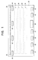
- FIG. 1 is a plan view of the invented light-emitting array, showing the surface of the driver IC without the electroluminescent elements.
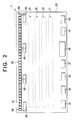
- FIG. 2 is a plan view of the same light-emitting array, showing the electroluminescent elements.
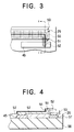
- FIG. 3 is an enlarged plan view of the section marked P in FIG. 2.
- FIG. 4 is a sectional view through line I-I in FIG. 3.
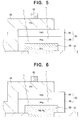
- FIG. 5 is a sectional view illustrating the structure of an electroluminescent element in a first embodiment of the invented light-emitting array.
- FIG. 6 illustrates the structure of an electroluminescent element in a second embodiment.
- FIG. 7 illustrates the structure of an electroluminescent element in a third embodiment.
- FIG. 8 illustrates the structure of an electroluminescent element in a fourth embodiment.
- FIG. 9 illustrates the structure of an electroluminescent element in a fifth embodiment.
- FIG. 10 illustrates the structure of an electroluminescent element in a sixth embodiment.
- FIG. 11 illustrates the structure of an electroluminescent element in a seventh embodiment.
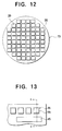
- FIG. 12 illustrates a step in a fabrication process for the invented light-emitting array.
- FIG. 13 illustrates another step in this fabrication process.
- FIG. 14 is a sectional view through line II-II in FIG. 7.
- FIG. 15 illustrates another step in the same fabrication process.
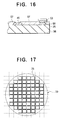
- FIG. 16 is a sectional view through line III-III in FIG. 9.
- FIG. 17 illustrates a final fabrication step
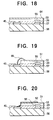
- FIG. 18 illustrates a step in an alternative fabrication process for the invented light-emitting array.
- FIG. 19 illustrates another step in this alternative fabrication process.
- FIG. 20 illustrates a variation of the alternative fabrication process.
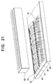
- FIG. 21 is a perspective view of the main parts of the invented optical head assembly.
- FIGs. 1 to 4 apply to all of the illustrated embodiments of the invented light-emitting array.
- the invented light-emitting array comprises an integrated circuit, referred to below as the driver IC, with organic electroluminescent elements formed on one surface.
- FIG. 1 shows this surface of the driver IC 20, with the electroluminescent elements removed for better visibility of the IC structure.
- the integrated circuit comprises a shift register 21, a latch circuit 23, a logic circuit 25, a drive circuit 27, and a plurality of output terminals 29.
- the output terminals 29 are electrically coupled to respective drive elements such as transistors in the drive circuit 27.
- the internal structure of the shift register 21, latch circuit 23, logic circuit 25, and drive circuit 27 will not be described, as these circuits are well known.
- FIG. 1 Also shown in FIG. 1 are a clock signal input pad 31, data signal input pad 33, load signal input pad 35, strobe signal input pad 37, power supply pad 39, clock signal output pad 41, data signal output pad 43, and four common return pads 45.
- the sizes and shapes of these pads may vary depending on the design, but the power supply pad 39 and common return pads 45 are preferably of sufficient size to permit the connection of a plurality of bonding wires, because these pads carry the direct-current flow that powers all the electroluminescent elements.
- FIG. 2 shows the invented light-emitting array with the organic electroluminescent elements 50 in place.
- Components of the driver IC 20 are identified by the same reference numerals as in FIG. 1.
- One organic electroluminescent element 50 is formed over each of the output terminals 29 that were shown in FIG. 1.
- a common electrode 51 electrically couples all of the electroluminescent elements 50 to all of the common return pads 45. The reason for having multiple common return pads 45 is to reduce the voltage drop that occurs along the length of the common electrode 51 due to the resistance of the common electrode 51.
- FIG. 3 is an enlarged plan view of the part marked P in FIG. 2, showing the structure of the organic electroluminescent elements in more detail.
- a common metal electrode 52 runs as a longitudinal stripe down the center of the common electrode 51.
- the common metal electrode 52 further reduces the voltage drop along the length of the common electrode 51, and provides protection against possible open circuits that might form in the common electrode 51 due to irregularities in the underlying surface.
- the common electrode 51 makes electrical contact with an organic electroluminescent film 53, which extends the length of the light-emitting array. This film will be referred to below as an organic EL film. Electrical connection between the organic EL film 53 and each output terminal 29 is effected by a corresponding individual electrode 55.
- a single organic electroluminescent element consists of one individual electrode 55 and the part of the organic EL film 53 and common electrode 51 disposed over or immediately adjacent to that individual electrode 55.
- FIG. 4 is a sectional view through line I-I in FIG. 3, omitting the circuits of the driver IC for simplicity. These circuits are formed in a semiconductor substrate 56, the output terminals 29 being formed on the surface of the substrate 56. A protective layer 57 on the surface of the substrate 56 protects the underlying integrated circuit, and insulates the circuit elements (not shown) from the common electrode 51 and common metal electrode 52.
- the output terminals 29 of silicon integrated circuits are generally fabricated from a metal-silicon alloy such as aluminum-silicon (Al-Si) or aluminum-silicon-copper (Al-Si-Cu), which has a large work function. This presents a problem when the output terminals 29 are on the cathode side, as in the first six embodiments described below.
- the individual electrodes 55 are a solution to this problem. Made of a material having a small work function, such as an aluminum-lithium or magnesium-silver alloy, they provide a suitable electrical interface between the output terminals 29 and organic EL film 53.
- An alternative solution is to make the output terminals 29 themselves from a material having a small work function, such as an aluminum-lithium alloy, or to make at least an upper layer of the output terminals 29 from such a material.
- the organic EL film 53 can make direct contact with the output terminals 29, and the individual electrodes 55 are unnecessary.
- This alternative solution has the advantage of simplifying the fabrication process.
- the individual electrodes 55 can also be omitted when the output terminals 29 are on the anode side of the electroluminescent elements 50, as will be shown in the seventh embodiment. In that case the common electrode 51 has a small work function.
- FIG. 5 is an enlarged sectional view showing the structure of the organic electroluminescent elements 50 in a first embodiment of the invention.
- the common electrode 51 is made of indium-tin-oxide (ITO), a well-known transparent conductive material having a large work function, with a thickness on the order of one or two tenths of micrometer (0.1 to 0.2 ⁇ m).
- the common metal electrode 52 is made of, for example, aluminum.
- the individual electrode 55 is an aluminum-lithium alloy with a preferred thickness in the range from fifty to two hundred nanometers (50 to 200 nm).
- the organic EL film 53 consists of two layers: an organic electron-transport layer 59 and an organic hole-transport layer 61. The electron-transport layer 59 makes contact with the individual electrode 55, while the hole-transport layer 61 is in contact with the common electrode 51.
- An electron-transport layer is a layer of a substance that readily permits the injection of electrons from an electrode having a small work function, and permits the injected electrons to move within the layer, but hinders the injection of holes, or permits the injection of holes but hinders their motion within the layer.
- the substance constituting the organic electron-transport layer 59 in the first embodiment is an aluminum-quinolinol complex, more specifically tris-(8-quinolinol)aluminum, abbreviated Alq3 below, which is also luminescent.
- the electron-transport layer 59 is deposited by evaporation to a thickness of 0.05 ⁇ m.
- a hole-transport layer is a layer of a substance that readily permits the injection of holes from an electrode having a large work function, and permits the injected holes to move within the layer, but hinders the injection of electrons, or permits the injection of electrons but hinders their motion within the layer.
- the organic hole-transport layer 61 in the first embodiment consists of a triphenyl amine derivative, more specifically N,N'-diphenyl-N,N'-bis(3-methylphenyl)-1,1'-biphenyl-4,4'-diamine, abbreviated TAD below.
- TAD triphenyl amine derivative
- the first embodiment operates as follows. Referring again to FIG. 2, dot data for a row of dots are input at pad 33 and clocked into the shift register 21 in synchronization with a clock signal input at pad 31. In response to a load signal input at pad 35, the dot data are transferred to the latch circuit 23. In response to a strobe signal input at pad 37, the dot data are supplied through the logic circuit 25 to the drive circuit 27, where they activate selected drive elements (e.g. transistors) that feed current from the power supply pad 39 to the corresponding electroluminescent elements 50. The current flow is direct, the output terminals 29 being at a lower potential than the common return pads 45. The output terminals 29 and individual electrodes 55 therefore function as the cathodes of the electroluminescent elements, while the common electrode 51 functions as the anode.
- selected drive elements e.g. transistors
- One advantage of the invented light-emitting array is that the potential difference required to drive the organic electroluminescent elements 50 is not large, being only about ten volts, as compared with the higher drive voltages required by conventional inorganic electroluminescent materials such as ZnS.
- the output terminals 29 and common return pads 45 can be placed at potentials of, for example, minus five volts and plus five volts, respectively, or the output terminals 29 can be placed at zero volts and the common return pads 45 at ten volts.
- the drive circuit 27 can easily be designed to withstand these voltages. There is no need to use alternating current.
- the driver IC 20 can be similar in design to the ICs commonly used to drive LED arrays.
- FIG. 6 shows the structure of the organic electroluminescent elements in a second embodiment of the invention.
- the structure is the same as in the first embodiment, except that the individual electrode 55 is a magnesium-silver film with a thickness of three hundred nanometers (300 nm), and the hole-transporting layer 61 consists of a triphenyldiamine substance (abbreviated TPD). Operation is the same as in the first embodiment.
- the second embodiment has produced optical brightness values on the order of 105 cd/m, when driven at voltages in the range from five to ten volts.
- FIG. 7 shows the structure of the organic electroluminescent elements in a third embodiment.
- the organic electron-transport layer 59 now consists of an oxadiazole derivative, more specifically the substance 2-(4-Biphenylyl)-5-(4-tert-butylphenyl)-1,3,4-oxadiazole, abbreviated PBD, which is non-luminescent.
- the hole-transport layer 61 consists of a triphenylamine derivative, more specifically the substance N,N-bis(4-methoxyphenyl)-4-[2-(1-naphthalenyl)ethenyl]-Benzenamine, abbreviated NSD, which is luminescent. Operation is as in the first embodiment, except that light is now emitted from the hole-transport layer 61 instead of from the electron-transport layer 59.
- FIG. 8 shows the structure of the organic electroluminescent elements in a fourth embodiment.
- the electron-transport layer 59 consists of PBD, as in the third embodiment.
- the hole-transport layer 61 consists of TAD, as in the first embodiment. Neither of these layers is luminescent, so an organic light-emitting layer 63 is inserted between them.
- the organic light-emitting layer 63 comprises anthracene, a substance that possesses bipolar mobility: the property of transporting both electrons and holes to the same degree. Operation is similar to the preceding embodiments. Electrons and holes are transported through layers 59 and 61, respectively, and recombine in the light-emitting layer 63, causing emission of light.
- the invention can be practiced with a variety of organic light-emitting substances, including substances with electron mobility, substances with hole mobility, and substances with bipolar mobility.
- FIG. 9 shows the structure of the organic electroluminescent elements in a fifth embodiment.
- the organic EL film 53 now comprises a single layer in which an electron-transporting organic compound, a hole-transporting organic compound, and a light-emitting organic compound are mixed together.
- the electron-transporting organic compound is an oxydiazole derivative, more specifically (2,5-bis-naphthyl-1,3,4-oxadiazole).
- the hole-transporting organic compound is hydrazone.
- the light-emitting organic compound is a polyester resin with an admixture of coumarin, a dye employed in lasers. These substances were selected to satisfy necessary conditions for balanced injection of electrons and holes, and for carrier recombination.
- the overall thickness of this organic EL film 53 is 0.2 ⁇ m.
- the fifth embodiment operates like the preceding embodiments, and has been found to give adequate emission of light.
- the mixed layer can be formed by dip-coating, using a solution of the above organic components with a gravimetric ratio of 1:1:1:0.05, that is, twenty parts oxydiazole derivative, twenty parts hydrazone, twenty parts polyester resin, and one part coumarin.
- Hydrazone incidentally, could also be used for the non-luminescent hole-transport layer in layered films such as those in the first, second, and fourth embodiments.
- FIG. 10 shows the structure of the organic electroluminescent elements in a sixth embodiment.
- the organic EL film 53 in this embodiment consists of a single conductive polymer layer, more specifically a layer of poly(3-octadecylthiophene) with a thickness of 0.2 ⁇ m, formed by spin-coating. This material appears to give well-balanced injection of electrons and holes from the individual electrode 55 and common electrode 51, respectively, and provides adequate emission of light.
- FIG. 11 shows the structure of the organic electroluminescent elements in a seventh embodiment. This embodiment differs from the previous embodiments in that light is emitted from the edges of the organic electroluminescent elements.
- the organic EL film 53 comprises a conductive polymer as in the sixth embodiment.
- the common electrode 51 does not have to be transparent, so it need not be made of a material such as ITO having a large work function.
- a material such as an aluminum-lithium alloy (as shown in the drawing), or a magnesium-silver alloy, which has a small work function, can be employed in the common electrode 51, and a material such as gold, which has as large work function, can be employed in the output terminal 29.
- the output terminal 29 can comprise a lower layer 29a of aluminum-silicon and an upper layer 29b of gold, as shown in the drawing. Alternatively, the entire output terminal 29 could be made of gold.
- the common electrode 51 is made of the comparatively high-resistance material ITO, as in the first six embodiments, supplying driving current through the common electrode 51 alone, without the common metal electrode 52, would lead to an undesired voltage drop at intermediate points between the common return pads 45.
- the common electrode 51 is made of a low-resistance material such as an aluminum-lithium or magnesium-silver alloy, however, as in the seventh embodiment, less voltage drop occurs, and the common metal electrode 52 can be omitted.
- the seventh embodiment operates like the sixth embodiment, except that light is emitted sideways from the edge of the organic EL film 53, and the electrical polarity is reversed. Since the gold surface layer 29b of the output terminal 29 has a large work function and the magnesium-silver common electrode 51 has a small work function, the output terminal 29 is now driven at a higher voltage than the common electrode 51, so that the common electrode 51 is the cathode and supplies electrons, while the output terminal 29 is the anode and supplies holes.
- a large number of identical driver ICs 20 are first fabricated in a semiconductor wafer 70.
- the wafer 70 is preferably a silicon wafer.
- CMOS complementary metal-oxide-semiconductor
- bipolar, or bipolar metal-oxide-semiconductor (biMOS) technologies are available, such as the well-known complementary metal-oxide-semiconductor (CMOS). bipolar, or bipolar metal-oxide-semiconductor (biMOS) technologies.
- Fabrication of the driver ICs 20 includes formation of the output terminals 29, protective layer 57, common return pads 45, and the other pads that were shown in FIGs. 1 to 4.
- the individual electrodes 55 are created, using a standard photolithographic lift-off technique. Specifically, the wafer 70 is coated with a photoresist (not shown), which is patterned to create windows at the sites where the individual electrodes 55 are to be formed. A thin film of the electrode material (e.g. an aluminum-lithium or magnesium-silver alloy, or gold) is next deposited over the entire wafer 70. The patterned photoresist is then lifted off, leaving the desired individual electrodes 55.
- FIG. 13 shows the result in plan view
- FIG. 14 shows a sectional view through line II-II in FIG. 13.
- the organic EL film 53 is created, using a similar lift-off technique.
- the wafer 70 is coated with another photoresist (not shown) which is patterned to leave a window in the desired shape of the organic EL film 53 on each driver IC 20.
- the layer or layers constituting the organic EL film 53 are then formed over the entire surface of the wafer 70.
- layers of ALq3 and TAD can be successively deposited by the resistive-heating evaporation deposition method under vacuum conditions, the ambient pressure not exceeding 10 ⁇ 3 Pascals.
- the wafer 70 need not be heated or cooled.
- Similar layer deposition processes can be used in the second, third, and fourth embodiments.
- the single organic layer in the fifth or sixth embodiment can be formed by dip-coating or spin-coating, as mentioned earlier.
- FIG. 15 shows the result in plan view
- FIG. 16 shows a sectional view through line III-III in FIG. 15.
- the wafer 70 is diced along the dotted lines shown in FIG. 17, each resulting die being a completed organic light-emitting array 75 with integral driving circuits.
- This alternative process differs from the process described above only in the patterning of the organic EL film 53 and common electrodes 51.
- a conductive film 64 comprising, for example, ITO or an aluminum-lithium alloy is deposited on the entire surface of the organic EL film 53.
- the organic EL film 53 and conductive film 64 are then patterned simultaneously. as follows. First, a photoresist (not shown) is coated onto the wafer over the conductive film 64 and patterned. Next, the parts of the conductive film 64 and organic EL film 53 not protected by the photoresist are removed by, for example, dry etching. Finally, the photoresist pattern is removed, leaving the configuration shown in FIG. 19. The remaining part of the conductive film 64 becomes the common electrode 51.
- the common electrode 51 comprises a material suitable for wire bonding, however, such as the aluminum-lithium or magnesium-silver alloy of the seventh embodiment, the common electrode 51 can be coupled to the common return pads 45 by attaching bonding wires 65 as shown in FIG. 19.
- the wire bonding can be performed together with other wire bonding after the wafer has been diced, when the individual arrays are installed.
- the electrical connection to the common return pads 45 can be effected by means of the common metal electrode 52 described earlier.
- the common metal electrode 52 is patterned so as to extend onto the common return pads 45, as well as forming a stripe on the common electrode 51.
- the alternative fabrication process has the advantage of requiring fewer photolithography steps, since the organic EL film 53 and common electrode 51 are patterned simultaneously.
- FIG. 21 shows the main parts of the head assembly in perspective view.
- the optical head assembly comprises a printed circuit board 81 of, for example, the common glass-epoxy type, on which are mounted a plurality of organic electroluminescent light-emitting arrays 75 of the type shown in any of the preceding embodiments.
- the arrays 75 are die-bonded to the printed circuit board 81 in an end-to-end configuration, so that their electroluminescent elements are arranged in a single linear array.
- a lens array 83 is mounted facing the array of electroluminescent elements, to focus the emitted light. (The mounting structure of the lens array 83 has been omitted to simplify the drawing.)
- the lens array 83 depicted in FIG. 21 is of the well-known self-focusing (selfoc) type, but the invention is not restricted to any particular type of lens array. In some applications the lens array is unnecessary, and can be omitted.
- the common return pads 45 and other pads on the organic light-emitting arrays 75 are coupled by bonding wires 85 (made of gold. for example) to printed wiring traces 87 on the printed circuit board 81. These traces 87 supply power and signals to the light-emitting arrays 75.
- the clock and data output pads of each light-emitting array 75 are coupled by the bonding wires and traces to the clock and data input pads of the next array 75, so that dot data can be shifted serially through all the shift registers 21 in the arrays.
- One advantage of the invented optical head assembly is that it requires relatively little wire bonding. No bonding wires are needed to connect the light-emitting elements to their drive circuits. This reduces the cost of manufacturing the optical head assembly, and improves its reliability by reducing the risk of short circuits between bonding wires.
- Another advantage is a reduced parts count and reduced amount of die bonding, again as compared with a conventional LED head, because the light-emitting elements and their driving circuits are on the same dies. This further reduces the cost of manufacturing the optical head assembly, and reduces its size.
- the parts count and hence the manufacturing cost of the optical head assembly can be reduced still further by making the individual arrays themselves large, so that fewer of them are needed to obtain a combined array of a given total width.
- Yet another advantage over a conventional LED head is that extremely high dot resolutions can be achieved. Since the dot pitch is not limited by the need to allow space between bonding wires, the electroluminescent elements can be placed as close together as their size permits. Dot resolutions in excess of one thousand two hundred dots per inch (1200 DPI) can be anticipated. Photolithography can define features smaller than one micrometer (1 ⁇ m), so dot resolutions exceeding ten thousand dots per inch may be within reach.
- the invention is not restricted to the materials and methods described in the embodiments above.
- Other electron-transporting luminescent substances may be used in the organic EL film 53, for example, including porphyrin and various other metallic complexes, beryllium-benzoquinolinol, cyclopentadiene derivatives, and perylene derivatives, to name just a few.
- Other possible hole-transporting substances include, for example, triphenylmethane, oxadiazole, pyrazoline, and polyvinyl carbazole substances.
- organic electroluminescent compounds In selecting organic electroluminescent compounds. the guidelines should be high brightness, high efficiency. long life, and suitability for fine patterning. Small amounts of dye substances can be added, as coumarin was added in the fifth embodiment, to improve electroluminescent efficiency, or to match the emitted wavelength of light to the sensitive band of the material to be illuminated (e.g. the photosensitive drum in an electrophotographic printer).
- Thin films of the selected organic compounds can be formed by vacuum evaporation, dip-coating, or spin-coating as mentioned above, or by other methods such as organic molecular beam deposition (OMBD), plasma polymerization, micellar electrolysis, or the Langmuir-Blodgett method, depending on design considerations.
- OMBD organic molecular beam deposition
- plasma polymerization plasma polymerization
- micellar electrolysis micellar electrolysis
- Langmuir-Blodgett method depending on design considerations.
- GaAs gallium arsenide
- InP indium phosphide
- AlGaAs aluminum-gallium arsenide
- GaP gallium phosphide
Landscapes
- Physics & Mathematics (AREA)
- Optics & Photonics (AREA)
- Health & Medical Sciences (AREA)
- General Health & Medical Sciences (AREA)
- Toxicology (AREA)
- Electroluminescent Light Sources (AREA)
- Printers Or Recording Devices Using Electromagnetic And Radiation Means (AREA)
- Led Device Packages (AREA)
- Led Devices (AREA)
- Facsimile Heads (AREA)
Applications Claiming Priority (2)
| Application Number | Priority Date | Filing Date | Title |
|---|---|---|---|
| JP231507/94 | 1994-09-27 | ||
| JP23150794A JPH0890832A (ja) | 1994-09-27 | 1994-09-27 | 発光素子アレイおよび光学ヘッド |
Publications (2)
| Publication Number | Publication Date |
|---|---|
| EP0704915A1 true EP0704915A1 (fr) | 1996-04-03 |
| EP0704915B1 EP0704915B1 (fr) | 1998-12-16 |
Family
ID=16924582
Family Applications (1)
| Application Number | Title | Priority Date | Filing Date |
|---|---|---|---|
| EP95306773A Expired - Lifetime EP0704915B1 (fr) | 1994-09-27 | 1995-09-26 | Réseau électroluminescent organique et tête optique |
Country Status (4)
| Country | Link |
|---|---|
| US (1) | US6297842B1 (fr) |
| EP (1) | EP0704915B1 (fr) |
| JP (1) | JPH0890832A (fr) |
| DE (1) | DE69506655T2 (fr) |
Cited By (20)
| Publication number | Priority date | Publication date | Assignee | Title |
|---|---|---|---|---|
| EP0884782A1 (fr) * | 1996-06-10 | 1998-12-16 | Motorola, Inc. | Boítier électro-optique intégré et son procédé de fabrication |
| WO1999016289A1 (fr) * | 1997-09-24 | 1999-04-01 | Koninklijke Philips Electronics N.V. | Dispositif electroluminescent organique |
| EP0889435A3 (fr) * | 1997-06-30 | 1999-09-01 | Oki Electric Industry Co., Ltd. | Puce avec une rangée d'éléments à électroluminescence, circuit intégré de commande pour une rangée d'éléments à électroluminescence et tête d'impression |
| EP0916506A3 (fr) * | 1997-11-11 | 1999-09-08 | Canon Kabushiki Kaisha | Appareil de formation d'image |
| EP1044586A4 (fr) * | 1997-10-09 | 2000-11-08 | Univ Princeton | Cathodes non metalliques hautement transparentes |
| EP0917216A3 (fr) * | 1997-11-17 | 2000-11-08 | Lg Electronics Inc. | Dispositif organique électroluminescent avec stabilité à long terme améliorée |
| EP0982783A3 (fr) * | 1998-08-21 | 2000-11-08 | TDK Corporation | Dispositif organique électroluminescent et procédé de fabrication |
| EP1009046A3 (fr) * | 1998-10-22 | 2000-11-22 | Canon Kabushiki Kaisha | Rangée d'éléments à électroluminescence, dispositif d'exposition et appareil de formation d'images |
| US6303238B1 (en) | 1997-12-01 | 2001-10-16 | The Trustees Of Princeton University | OLEDs doped with phosphorescent compounds |
| EP1106366A3 (fr) * | 1999-12-02 | 2002-02-27 | Canon Kabushiki Kaisha | Tête à LED, appareil de formation d'images, et méthode de mesure de la quantité de lumière émise par des rangées de diodes électro-luminescentes |
| US6413656B1 (en) | 1998-09-14 | 2002-07-02 | The University Of Southern California | Reduced symmetry porphyrin molecules for producing enhanced luminosity from phosphorescent organic light emitting devices |
| US6420031B1 (en) | 1997-11-03 | 2002-07-16 | The Trustees Of Princeton University | Highly transparent non-metallic cathodes |
| US6451455B1 (en) | 1998-04-01 | 2002-09-17 | The Trustees Of Princeton University | Metal complexes bearing both electron transporting and hole transporting moieties |
| US6469437B1 (en) | 1997-11-03 | 2002-10-22 | The Trustees Of Princeton University | Highly transparent organic light emitting device employing a non-metallic cathode |
| RU2202843C2 (ru) * | 2001-04-27 | 2003-04-20 | Институт проблем химической физики РАН | Полупроводниковый электролюминесцентный источник света с перестраиваемым цветом свечения |
| EP1134816A3 (fr) * | 2000-03-17 | 2004-08-11 | Agilent Technologies, Inc. (a Delaware corporation) | Dispositif d'affichage électroluminescent organique et procédé pour structurer des cathodes pour un tel dispositif |
| US6830828B2 (en) | 1998-09-14 | 2004-12-14 | The Trustees Of Princeton University | Organometallic complexes as phosphorescent emitters in organic LEDs |
| US7001536B2 (en) | 1999-03-23 | 2006-02-21 | The Trustees Of Princeton University | Organometallic complexes as phosphorescent emitters in organic LEDs |
| US7847286B2 (en) | 1997-11-17 | 2010-12-07 | Lg Electronics Inc. | Semiconductor device |
| US10965831B2 (en) | 2017-05-25 | 2021-03-30 | Sony Semiconductor Solutions Corporation | Optical head, optical head scanning device, and method for driving optical head scanning device |
Families Citing this family (43)
| Publication number | Priority date | Publication date | Assignee | Title |
|---|---|---|---|---|
| JP2000164359A (ja) * | 1998-11-25 | 2000-06-16 | Idemitsu Kosan Co Ltd | 有機エレクトロルミネッセンス素子 |
| JP2001102626A (ja) * | 1999-07-28 | 2001-04-13 | Canon Inc | Ledチップ、ledアレイチップ、ledアレイヘッド及び画像形成装置 |
| US6693033B2 (en) | 2000-02-10 | 2004-02-17 | Motorola, Inc. | Method of removing an amorphous oxide from a monocrystalline surface |
| US6392257B1 (en) | 2000-02-10 | 2002-05-21 | Motorola Inc. | Semiconductor structure, semiconductor device, communicating device, integrated circuit, and process for fabricating the same |
| KR20030011083A (ko) | 2000-05-31 | 2003-02-06 | 모토로라 인코포레이티드 | 반도체 디바이스 및 이를 제조하기 위한 방법 |
| JP2001343803A (ja) * | 2000-06-01 | 2001-12-14 | Canon Inc | 画像形成装置 |
| WO2002009187A2 (fr) | 2000-07-24 | 2002-01-31 | Motorola, Inc. | Diodes a heterojonction tunnel et processus de fabrication de celles-ci |
| US6638838B1 (en) | 2000-10-02 | 2003-10-28 | Motorola, Inc. | Semiconductor structure including a partially annealed layer and method of forming the same |
| US6861091B2 (en) * | 2000-12-27 | 2005-03-01 | Canon Kabushiki Kaisha | Self-assembly of organic-inorganic nanocomposite thin films for use in hybrid organic light emitting devices (HLED) |
| US20020096683A1 (en) | 2001-01-19 | 2002-07-25 | Motorola, Inc. | Structure and method for fabricating GaN devices utilizing the formation of a compliant substrate |
| US6673646B2 (en) | 2001-02-28 | 2004-01-06 | Motorola, Inc. | Growth of compound semiconductor structures on patterned oxide films and process for fabricating same |
| CN100463484C (zh) * | 2001-03-29 | 2009-02-18 | 松下电器产业株式会社 | 图像写入装置,光源,光源单元,微透镜以及微透镜的制造方法 |
| WO2002082551A1 (fr) | 2001-04-02 | 2002-10-17 | Motorola, Inc. | Structure de semi-conducteur a courant de fuite attenue |
| US6709989B2 (en) | 2001-06-21 | 2004-03-23 | Motorola, Inc. | Method for fabricating a semiconductor structure including a metal oxide interface with silicon |
| US6992321B2 (en) | 2001-07-13 | 2006-01-31 | Motorola, Inc. | Structure and method for fabricating semiconductor structures and devices utilizing piezoelectric materials |
| US6646293B2 (en) | 2001-07-18 | 2003-11-11 | Motorola, Inc. | Structure for fabricating high electron mobility transistors utilizing the formation of complaint substrates |
| US6693298B2 (en) | 2001-07-20 | 2004-02-17 | Motorola, Inc. | Structure and method for fabricating epitaxial semiconductor on insulator (SOI) structures and devices utilizing the formation of a compliant substrate for materials used to form same |
| US7019332B2 (en) | 2001-07-20 | 2006-03-28 | Freescale Semiconductor, Inc. | Fabrication of a wavelength locker within a semiconductor structure |
| US6855992B2 (en) | 2001-07-24 | 2005-02-15 | Motorola Inc. | Structure and method for fabricating configurable transistor devices utilizing the formation of a compliant substrate for materials used to form the same |
| US6667196B2 (en) | 2001-07-25 | 2003-12-23 | Motorola, Inc. | Method for real-time monitoring and controlling perovskite oxide film growth and semiconductor structure formed using the method |
| US6639249B2 (en) | 2001-08-06 | 2003-10-28 | Motorola, Inc. | Structure and method for fabrication for a solid-state lighting device |
| US20030034491A1 (en) | 2001-08-14 | 2003-02-20 | Motorola, Inc. | Structure and method for fabricating semiconductor structures and devices for detecting an object |
| US6673667B2 (en) | 2001-08-15 | 2004-01-06 | Motorola, Inc. | Method for manufacturing a substantially integral monolithic apparatus including a plurality of semiconductor materials |
| US20030071327A1 (en) | 2001-10-17 | 2003-04-17 | Motorola, Inc. | Method and apparatus utilizing monocrystalline insulator |
| JP3730573B2 (ja) * | 2002-01-16 | 2006-01-05 | シャープ株式会社 | 露光装置および画像形成装置 |
| JP2003249380A (ja) * | 2002-02-26 | 2003-09-05 | Sanyo Electric Co Ltd | エレクトロルミネッセンス表示装置 |
| US6916717B2 (en) | 2002-05-03 | 2005-07-12 | Motorola, Inc. | Method for growing a monocrystalline oxide layer and for fabricating a semiconductor device on a monocrystalline substrate |
| JP3846367B2 (ja) * | 2002-05-30 | 2006-11-15 | セイコーエプソン株式会社 | 半導体素子部材及び半導体装置並びにそれらの製造方法、電気光学装置、電子機器 |
| US7169619B2 (en) | 2002-11-19 | 2007-01-30 | Freescale Semiconductor, Inc. | Method for fabricating semiconductor structures on vicinal substrates using a low temperature, low pressure, alkaline earth metal-rich process |
| US6885065B2 (en) | 2002-11-20 | 2005-04-26 | Freescale Semiconductor, Inc. | Ferromagnetic semiconductor structure and method for forming the same |
| JP2004170889A (ja) * | 2002-11-22 | 2004-06-17 | Seiko Epson Corp | 画像形成装置 |
| US6965128B2 (en) | 2003-02-03 | 2005-11-15 | Freescale Semiconductor, Inc. | Structure and method for fabricating semiconductor microresonator devices |
| US7020374B2 (en) | 2003-02-03 | 2006-03-28 | Freescale Semiconductor, Inc. | Optical waveguide structure and method for fabricating the same |
| US7286147B2 (en) | 2003-11-05 | 2007-10-23 | Seiko Epson Corporation | Line head and image forming device using the same |
| US7411601B2 (en) * | 2004-08-03 | 2008-08-12 | Seiko Epson Corporation | Exposure head |
| JP4211710B2 (ja) * | 2004-08-04 | 2009-01-21 | セイコーエプソン株式会社 | ラインヘッドモジュールおよび画像形成装置 |
| JP4327699B2 (ja) * | 2004-10-28 | 2009-09-09 | 富士通マイクロエレクトロニクス株式会社 | マルチチップ・パッケージおよびicチップ |
| JP4662798B2 (ja) * | 2005-03-24 | 2011-03-30 | 株式会社沖データ | 半導体複合装置、プリントヘッド、及び画像形成装置 |
| JP4920204B2 (ja) * | 2005-06-24 | 2012-04-18 | 富士電機株式会社 | 半導体装置 |
| JP4370321B2 (ja) * | 2006-12-05 | 2009-11-25 | 株式会社沖データ | 駆動装置、ledアレイ、ledヘッド、及びこれらを備えた画像形成装置 |
| DE102012220724B4 (de) * | 2012-11-14 | 2022-05-25 | Pictiva Displays International Limited | Optoelektronisches Bauelement |
| WO2017193316A1 (fr) * | 2016-05-11 | 2017-11-16 | Viewtrix Technology Co., Ltd. | Appareil d'affichage à diodes électroluminescentes organiques intégrées et ses procédés de fabrication |
| CN114270276A (zh) * | 2019-08-23 | 2022-04-01 | 佳能株式会社 | 具有顶部发射发光设备的图像形成装置 |
Citations (2)
| Publication number | Priority date | Publication date | Assignee | Title |
|---|---|---|---|---|
| US4829321A (en) * | 1987-04-23 | 1989-05-09 | Hitachi Cable, Ltd. | Optical printer head with a light emitting diode array |
| EP0572779A1 (fr) * | 1992-06-04 | 1993-12-08 | Motorola, Inc. | Source d'affichage intégré comprenant des polymères émetteurs de lumière |
Family Cites Families (22)
| Publication number | Priority date | Publication date | Assignee | Title |
|---|---|---|---|---|
| JPS5421695B1 (fr) * | 1969-06-14 | 1979-08-01 | ||
| US4887098A (en) * | 1988-11-25 | 1989-12-12 | Xerox Corporation | Thermal ink jet printer having printhead transducers with multilevelinterconnections |
| US5600363A (en) * | 1988-12-28 | 1997-02-04 | Kyocera Corporation | Image forming apparatus having driving means at each end of array and power feeding substrate outside head housing |
| US5099301A (en) | 1989-09-29 | 1992-03-24 | Yu Holding (Bvi), Inc. | Electroluminescent semiconductor device |
| FI84869C (fi) * | 1990-06-11 | 1992-01-27 | Planar Int Oy | Matrisfilmstruktur i synnerhet foer elektroluminecens displayenhet. |
| JPH0471194A (ja) | 1990-07-10 | 1992-03-05 | Fuji Xerox Co Ltd | Tft駆動elディスプレイ及びその製造方法 |
| US5371525A (en) * | 1990-11-30 | 1994-12-06 | Kyocera Corporation | Image head |
| US5661371A (en) * | 1990-12-31 | 1997-08-26 | Kopin Corporation | Color filter system for light emitting display panels |
| JPH04270666A (ja) | 1991-02-26 | 1992-09-28 | Tokyo Electric Co Ltd | 端面発光型elプリンタ及び製造方法 |
| JPH04280095A (ja) | 1991-03-06 | 1992-10-06 | Nippon Sheet Glass Co Ltd | 直流エレクトロルミネッセンス素子 |
| US5179316A (en) * | 1991-09-26 | 1993-01-12 | Mcnc | Electroluminescent display with space charge removal |
| US5652067A (en) * | 1992-09-10 | 1997-07-29 | Toppan Printing Co., Ltd. | Organic electroluminescent device |
| JP3300069B2 (ja) * | 1992-11-19 | 2002-07-08 | パイオニア株式会社 | 有機エレクトロルミネッセンス素子 |
| JP2845719B2 (ja) * | 1993-04-12 | 1999-01-13 | 沖電気工業株式会社 | ドライバic |
| US5405710A (en) * | 1993-11-22 | 1995-04-11 | At&T Corp. | Article comprising microcavity light sources |
| US5612549A (en) * | 1994-03-24 | 1997-03-18 | Motorola | Integrated electro-optical package |
| EP0681019B1 (fr) * | 1994-04-26 | 1999-09-01 | TDK Corporation | Dérivé de phenylanthracène et élément organique électroluminescent |
| JPH07314771A (ja) * | 1994-05-20 | 1995-12-05 | Sharp Corp | Led書込装置 |
| US5424560A (en) | 1994-05-31 | 1995-06-13 | Motorola, Inc. | Integrated multicolor organic led array |
| JP3246189B2 (ja) * | 1994-06-28 | 2002-01-15 | 株式会社日立製作所 | 半導体表示装置 |
| US5693962A (en) * | 1995-03-22 | 1997-12-02 | Motorola | Full color organic light emitting diode array |
| US5736754A (en) * | 1995-11-17 | 1998-04-07 | Motorola, Inc. | Full color organic light emitting diode array |
-
1994
- 1994-09-27 JP JP23150794A patent/JPH0890832A/ja not_active Withdrawn
-
1995
- 1995-09-21 US US08/531,753 patent/US6297842B1/en not_active Expired - Lifetime
- 1995-09-26 DE DE69506655T patent/DE69506655T2/de not_active Expired - Fee Related
- 1995-09-26 EP EP95306773A patent/EP0704915B1/fr not_active Expired - Lifetime
Patent Citations (2)
| Publication number | Priority date | Publication date | Assignee | Title |
|---|---|---|---|---|
| US4829321A (en) * | 1987-04-23 | 1989-05-09 | Hitachi Cable, Ltd. | Optical printer head with a light emitting diode array |
| EP0572779A1 (fr) * | 1992-06-04 | 1993-12-08 | Motorola, Inc. | Source d'affichage intégré comprenant des polymères émetteurs de lumière |
Non-Patent Citations (3)
| Title |
|---|
| BURROWS P E ET AL: "Metal ion dependent luminescence effects in metal tris-quinolate organic heterojunction light emitting devices", APPLIED PHYSICS LETTERS, 16 MAY 1994, USA, vol. 64, no. 20, ISSN 0003-6951, pages 2718 - 2720, XP000449711, DOI: doi:10.1063/1.111453 * |
| CHIHAYA ADACHI ET AL: "CONFINEMENT OF CHARGE CARRIERS AND MOLECULAR EXCITONS WITHIN 5-NM-THICK EMITTER LAYER IN ORGANIC ELECTROLUMINESCENT DEVICES WITH A DOUBLE HETEROSTRUCTURE", APPLIED PHYSICS LETTERS, vol. 57, no. 6, 6 August 1990 (1990-08-06), pages 531 - 533, XP000150169 * |
| YUTAKA OHMORI ET AL: "TIME-RESOLVED PULSE RESPONSE OF ELECTROLUMINESCENCE IN POLY(3-ALKYLTHIOPHENE) DIODES", JAPANESE JOURNAL OF APPLIED PHYSICS, vol. 31, no. 5A, 1 May 1992 (1992-05-01), pages L568 - L570, XP000323058 * |
Cited By (40)
| Publication number | Priority date | Publication date | Assignee | Title |
|---|---|---|---|---|
| EP0884782A1 (fr) * | 1996-06-10 | 1998-12-16 | Motorola, Inc. | Boítier électro-optique intégré et son procédé de fabrication |
| EP0889435A3 (fr) * | 1997-06-30 | 1999-09-01 | Oki Electric Industry Co., Ltd. | Puce avec une rangée d'éléments à électroluminescence, circuit intégré de commande pour une rangée d'éléments à électroluminescence et tête d'impression |
| US6172701B1 (en) | 1997-06-30 | 2001-01-09 | Oki Data Corporation | Light emitting element array chip, light emitting element array drive IC and print head |
| WO1999016289A1 (fr) * | 1997-09-24 | 1999-04-01 | Koninklijke Philips Electronics N.V. | Dispositif electroluminescent organique |
| EP1044586A4 (fr) * | 1997-10-09 | 2000-11-08 | Univ Princeton | Cathodes non metalliques hautement transparentes |
| US6420031B1 (en) | 1997-11-03 | 2002-07-16 | The Trustees Of Princeton University | Highly transparent non-metallic cathodes |
| US6469437B1 (en) | 1997-11-03 | 2002-10-22 | The Trustees Of Princeton University | Highly transparent organic light emitting device employing a non-metallic cathode |
| EP0916506A3 (fr) * | 1997-11-11 | 1999-09-08 | Canon Kabushiki Kaisha | Appareil de formation d'image |
| US6236416B1 (en) | 1997-11-11 | 2001-05-22 | Canon Kabushiki Kaisha | Image forming apparatus featuring a plurality of light emission elements on a single chip |
| EP0917216A3 (fr) * | 1997-11-17 | 2000-11-08 | Lg Electronics Inc. | Dispositif organique électroluminescent avec stabilité à long terme améliorée |
| US7847286B2 (en) | 1997-11-17 | 2010-12-07 | Lg Electronics Inc. | Semiconductor device |
| US6579632B2 (en) | 1997-12-01 | 2003-06-17 | The Trustees Of Princeton University | OLEDs doped with phosphorescent compounds |
| US6872477B2 (en) | 1997-12-01 | 2005-03-29 | The Trustees Of Princeton University | OLEDs doped with phosphorescent compounds |
| US9508940B2 (en) | 1997-12-01 | 2016-11-29 | The Trustees Of Princeton University | OLEDs doped with phosphorescent compounds |
| US7279237B2 (en) | 1997-12-01 | 2007-10-09 | The Trustees Of Princeton University | OLEDs doped with phosphorescent compounds |
| US6303238B1 (en) | 1997-12-01 | 2001-10-16 | The Trustees Of Princeton University | OLEDs doped with phosphorescent compounds |
| US7901795B2 (en) | 1997-12-01 | 2011-03-08 | The Trustees Of Princeton University | OLEDs doped with phosphorescent compounds |
| US7279235B2 (en) | 1997-12-01 | 2007-10-09 | The Trustees Of Princeton University | OLEDs doped with phosphorescent compounds |
| US7563519B2 (en) | 1997-12-01 | 2009-07-21 | The Trustees of Frinceton University | OLEDs doped with phosphorescent compounds |
| US7488542B2 (en) | 1997-12-01 | 2009-02-10 | The Trustees Of Princeton University | OLEDs doped with phosphorescent compounds |
| US6451455B1 (en) | 1998-04-01 | 2002-09-17 | The Trustees Of Princeton University | Metal complexes bearing both electron transporting and hole transporting moieties |
| US6339290B1 (en) | 1998-08-21 | 2002-01-15 | Tdk Corporation | Organic electroluminescent device and making method |
| EP0982783A3 (fr) * | 1998-08-21 | 2000-11-08 | TDK Corporation | Dispositif organique électroluminescent et procédé de fabrication |
| US6902830B2 (en) | 1998-09-14 | 2005-06-07 | The Trustees Of Princeton University | Organometallic complexes as phosphorescent emitters in organic LEDs |
| US6830828B2 (en) | 1998-09-14 | 2004-12-14 | The Trustees Of Princeton University | Organometallic complexes as phosphorescent emitters in organic LEDs |
| US6413656B1 (en) | 1998-09-14 | 2002-07-02 | The University Of Southern California | Reduced symmetry porphyrin molecules for producing enhanced luminosity from phosphorescent organic light emitting devices |
| EP1009046A3 (fr) * | 1998-10-22 | 2000-11-22 | Canon Kabushiki Kaisha | Rangée d'éléments à électroluminescence, dispositif d'exposition et appareil de formation d'images |
| US6344661B1 (en) | 1998-10-22 | 2002-02-05 | Canon Kabushiki Kaisha | Light emitting element array, exposure device and image forming apparatus |
| US7883787B2 (en) | 1999-03-23 | 2011-02-08 | The Trustees Of Princeton University | Organometallic complexes as phosphorescent emitters in organic LEDs |
| US7291406B2 (en) | 1999-03-23 | 2007-11-06 | The Trustees Of Princeton University | Organometallic complexes as phosphorescent emitters in organic LEDS |
| US7537844B2 (en) | 1999-03-23 | 2009-05-26 | The Trustees Of Princeton University | Organometallic complexes as phosphorescent emitters in organic leds |
| US7001536B2 (en) | 1999-03-23 | 2006-02-21 | The Trustees Of Princeton University | Organometallic complexes as phosphorescent emitters in organic LEDs |
| US8557402B2 (en) | 1999-03-23 | 2013-10-15 | The Trustees Of Princeton University | Organometallic complexes as phosphorescent emitters in organic LEDs |
| US8574726B2 (en) | 1999-03-23 | 2013-11-05 | The Trustees Of Princeton University | Organometallic complexes as phosphorescent emitters in organic LEDs |
| US10629827B2 (en) | 1999-03-23 | 2020-04-21 | The Trustees Of Princeton University | Organometallic complexes as phosphorescent emitters in organic LEDs |
| US6473106B2 (en) | 1999-12-02 | 2002-10-29 | Canon Kabushiki Kaisha | LED head, image forming apparatus, and method of measuring amount of light from LED array |
| EP1106366A3 (fr) * | 1999-12-02 | 2002-02-27 | Canon Kabushiki Kaisha | Tête à LED, appareil de formation d'images, et méthode de mesure de la quantité de lumière émise par des rangées de diodes électro-luminescentes |
| EP1134816A3 (fr) * | 2000-03-17 | 2004-08-11 | Agilent Technologies, Inc. (a Delaware corporation) | Dispositif d'affichage électroluminescent organique et procédé pour structurer des cathodes pour un tel dispositif |
| RU2202843C2 (ru) * | 2001-04-27 | 2003-04-20 | Институт проблем химической физики РАН | Полупроводниковый электролюминесцентный источник света с перестраиваемым цветом свечения |
| US10965831B2 (en) | 2017-05-25 | 2021-03-30 | Sony Semiconductor Solutions Corporation | Optical head, optical head scanning device, and method for driving optical head scanning device |
Also Published As
| Publication number | Publication date |
|---|---|
| EP0704915B1 (fr) | 1998-12-16 |
| DE69506655D1 (de) | 1999-01-28 |
| JPH0890832A (ja) | 1996-04-09 |
| DE69506655T2 (de) | 1999-07-01 |
| US6297842B1 (en) | 2001-10-02 |
Similar Documents
| Publication | Publication Date | Title |
|---|---|---|
| US6297842B1 (en) | Organic electroluminescent light-emitting array and optical head assembly | |
| EP0687019B1 (fr) | Matrice intégrée de diodes électroluminescentes multicolores organiques et procédé de fabrication | |
| US7923737B2 (en) | Three-terminal switch array device, combined semiconductor device, and image forming apparatus | |
| EP2287912B1 (fr) | Appareil LED composite à semiconducteur | |
| US5684368A (en) | Smart driver for an array of LEDs | |
| US8415680B2 (en) | Semiconductor composite apparatus, print head, and image forming apparatus | |
| US6140766A (en) | Organic EL device | |
| JP2807910B2 (ja) | 発光素子アレイ | |
| CN102683376A (zh) | 高压发光体、发光体及照明装置 | |
| EP1468832B1 (fr) | Dispositif d'exposition et dispositif d'imagerie | |
| US6791260B2 (en) | Organic electroluminescent element, panel and apparatus using the same | |
| JP2004134282A (ja) | 照明装置及びそれを用いた画像読取装置 | |
| US6717182B1 (en) | Edge-emitting light-emitting device having improved external luminous efficiency and self-scanning light-emitting device array comprising the same | |
| US8022418B2 (en) | Composite semiconductor device, LED print head that employs the composite semiconductor device, and image forming apparatus that employs the LED print head | |
| JP4161374B2 (ja) | 電気光学装置及び電子機器 | |
| US20080030133A1 (en) | Light-emitting structures | |
| US6919583B2 (en) | End surface light-emitting element having increased external light emission efficiency and self-scanning light-emitting element array using the same | |
| JP3696276B2 (ja) | 一次元配列有機el発光素子アレイヘッド及びその製造方法 | |
| JP2007250958A (ja) | 発光素子アレイ | |
| KR20010051879A (ko) | 유기 발광 소자 어레이 | |
| JP4744905B2 (ja) | 自発光表示パネル及びその製造方法 | |
| US20230005961A1 (en) | Display device and manufacturing method of the same | |
| JP3067783U (ja) | 自己走査型発光装置 | |
| JP2001060718A (ja) | 発光サイリスタおよび自己走査型発光装置 | |
| JP2004227975A (ja) | 有機エレクトロルミネッセンス素子を用いた光プリンタヘッド及び画像形成装置 |
Legal Events
| Date | Code | Title | Description |
|---|---|---|---|
| PUAI | Public reference made under article 153(3) epc to a published international application that has entered the european phase |
Free format text: ORIGINAL CODE: 0009012 |
|
| AK | Designated contracting states |
Kind code of ref document: A1 Designated state(s): DE FR GB |
|
| 17P | Request for examination filed |
Effective date: 19960812 |
|
| 17Q | First examination report despatched |
Effective date: 19970611 |
|
| GRAG | Despatch of communication of intention to grant |
Free format text: ORIGINAL CODE: EPIDOS AGRA |
|
| GRAG | Despatch of communication of intention to grant |
Free format text: ORIGINAL CODE: EPIDOS AGRA |
|
| GRAH | Despatch of communication of intention to grant a patent |
Free format text: ORIGINAL CODE: EPIDOS IGRA |
|
| GRAH | Despatch of communication of intention to grant a patent |
Free format text: ORIGINAL CODE: EPIDOS IGRA |
|
| GRAA | (expected) grant |
Free format text: ORIGINAL CODE: 0009210 |
|
| AK | Designated contracting states |
Kind code of ref document: B1 Designated state(s): DE FR GB |
|
| ET | Fr: translation filed | ||
| REF | Corresponds to: |
Ref document number: 69506655 Country of ref document: DE Date of ref document: 19990128 |
|
| PG25 | Lapsed in a contracting state [announced via postgrant information from national office to epo] |
Ref country code: GB Free format text: LAPSE BECAUSE OF NON-PAYMENT OF DUE FEES Effective date: 19990926 |
|
| PLBE | No opposition filed within time limit |
Free format text: ORIGINAL CODE: 0009261 |
|
| STAA | Information on the status of an ep patent application or granted ep patent |
Free format text: STATUS: NO OPPOSITION FILED WITHIN TIME LIMIT |
|
| 26N | No opposition filed | ||
| GBPC | Gb: european patent ceased through non-payment of renewal fee |
Effective date: 19990926 |
|
| PG25 | Lapsed in a contracting state [announced via postgrant information from national office to epo] |
Ref country code: FR Free format text: LAPSE BECAUSE OF NON-PAYMENT OF DUE FEES Effective date: 20000531 |
|
| PG25 | Lapsed in a contracting state [announced via postgrant information from national office to epo] |
Ref country code: DE Free format text: LAPSE BECAUSE OF NON-PAYMENT OF DUE FEES Effective date: 20000701 |
|
| REG | Reference to a national code |
Ref country code: FR Ref legal event code: ST |