EP0884783A2 - Mikromagnetische Vorrichtung zur Stromversorgung und ihr Herstellungsverfahren - Google Patents
Mikromagnetische Vorrichtung zur Stromversorgung und ihr Herstellungsverfahren Download PDFInfo
- Publication number
- EP0884783A2 EP0884783A2 EP98304525A EP98304525A EP0884783A2 EP 0884783 A2 EP0884783 A2 EP 0884783A2 EP 98304525 A EP98304525 A EP 98304525A EP 98304525 A EP98304525 A EP 98304525A EP 0884783 A2 EP0884783 A2 EP 0884783A2
- Authority
- EP
- European Patent Office
- Prior art keywords
- ferromagnetic core
- insulator
- recited
- layer
- depositing
- Prior art date
- Legal status (The legal status is an assumption and is not a legal conclusion. Google has not performed a legal analysis and makes no representation as to the accuracy of the status listed.)
- Withdrawn
Links
Images


Classifications
-
- H—ELECTRICITY
- H01—ELECTRIC ELEMENTS
- H01F—MAGNETS; INDUCTANCES; TRANSFORMERS; SELECTION OF MATERIALS FOR THEIR MAGNETIC PROPERTIES
- H01F17/00—Fixed inductances of the signal type
- H01F17/0006—Printed inductances
-
- H—ELECTRICITY
- H10—SEMICONDUCTOR DEVICES; ELECTRIC SOLID-STATE DEVICES NOT OTHERWISE PROVIDED FOR
- H10W—GENERIC PACKAGES, INTERCONNECTIONS, CONNECTORS OR OTHER CONSTRUCTIONAL DETAILS OF DEVICES COVERED BY CLASS H10
- H10W44/00—Electrical arrangements for controlling or matching impedance
- H10W44/501—Inductive arrangements
-
- H—ELECTRICITY
- H01—ELECTRIC ELEMENTS
- H01F—MAGNETS; INDUCTANCES; TRANSFORMERS; SELECTION OF MATERIALS FOR THEIR MAGNETIC PROPERTIES
- H01F41/00—Apparatus or processes specially adapted for manufacturing or assembling magnets, inductances or transformers; Apparatus or processes specially adapted for manufacturing materials characterised by their magnetic properties
- H01F41/02—Apparatus or processes specially adapted for manufacturing or assembling magnets, inductances or transformers; Apparatus or processes specially adapted for manufacturing materials characterised by their magnetic properties for manufacturing cores, coils, or magnets
- H01F41/04—Apparatus or processes specially adapted for manufacturing or assembling magnets, inductances or transformers; Apparatus or processes specially adapted for manufacturing materials characterised by their magnetic properties for manufacturing cores, coils, or magnets for manufacturing coils
- H01F41/041—Printed circuit coils
- H01F41/046—Printed circuit coils structurally combined with ferromagnetic material
-
- H—ELECTRICITY
- H10—SEMICONDUCTOR DEVICES; ELECTRIC SOLID-STATE DEVICES NOT OTHERWISE PROVIDED FOR
- H10D—INORGANIC ELECTRIC SEMICONDUCTOR DEVICES
- H10D86/00—Integrated devices formed in or on insulating or conducting substrates, e.g. formed in silicon-on-insulator [SOI] substrates or on stainless steel or glass substrates
- H10D86/80—Integrated devices formed in or on insulating or conducting substrates, e.g. formed in silicon-on-insulator [SOI] substrates or on stainless steel or glass substrates characterised by multiple passive components, e.g. resistors, capacitors or inductors
- H10D86/85—Integrated devices formed in or on insulating or conducting substrates, e.g. formed in silicon-on-insulator [SOI] substrates or on stainless steel or glass substrates characterised by multiple passive components, e.g. resistors, capacitors or inductors characterised by only passive components
-
- H—ELECTRICITY
- H10—SEMICONDUCTOR DEVICES; ELECTRIC SOLID-STATE DEVICES NOT OTHERWISE PROVIDED FOR
- H10W—GENERIC PACKAGES, INTERCONNECTIONS, CONNECTORS OR OTHER CONSTRUCTIONAL DETAILS OF DEVICES COVERED BY CLASS H10
- H10W20/00—Interconnections in chips, wafers or substrates
- H10W20/40—Interconnections external to wafers or substrates, e.g. back-end-of-line [BEOL] metallisations or vias connecting to gate electrodes
- H10W20/497—Inductive arrangements or effects of, or between, wiring layers
-
- H—ELECTRICITY
- H10—SEMICONDUCTOR DEVICES; ELECTRIC SOLID-STATE DEVICES NOT OTHERWISE PROVIDED FOR
- H10W—GENERIC PACKAGES, INTERCONNECTIONS, CONNECTORS OR OTHER CONSTRUCTIONAL DETAILS OF DEVICES COVERED BY CLASS H10
- H10W44/00—Electrical arrangements for controlling or matching impedance
- H10W44/601—Capacitive arrangements
Definitions
- the present invention is directed, in general, to micromagnetic devices and, more specifically, to a micromagnetic device for power processing applications, a method of manufacture therefor and a power processing circuit employing the same.
- a magnetic device includes a magnetic core coupled to conductor windings such that the magnetic flux flows in a closed path about the core.
- Magnetic devices are generally configured in an EE-type arrangement or a toroidal geometry.
- a first and second core-portion of the magnetic core surround the conductor windings.
- a first and second winding-portion of the conductor windings surround the magnetic core.
- Micromagnetic devices e.g., microinductors or microtransformers
- micromagnetic devices are micron-scaled integrated circuit magnetic devices; the electromagnetic properties of the device are provided by the presence of the magnetic core and conductor windings.
- micromagnetic devices were only applicable to low-level signal applications (e.g. , recording heads).
- micromagnetic devices may be employed in power systems for wireless communications equipment.
- the materials must be fabricated in inordinately thin films. Processing thin-film ferromagnetic materials with traditional rolling and tape winding techniques proves to be very costly as the desired tape thicknesses drops below 0.001 inches ( i.e., 25 ⁇ m). It is thus advantageous to produce such thin films by other integrated circuit deposition techniques such as sputtering or electroplating.
- Another germane consideration associated with manufacturing micromagnetic devices is securing the ferromagnetic material to a silicon substrate or the like. More specifically, forming an adequate bond between the ferromagnetic material and an insulator coupled to the substrate is an important consideration. Many factors such as oxide formation, melting point temperature, interposed contamination, affinity between materials and mechanical stress at the interface, influence the adhesion of a thin film to a substrate. For instance, one technique readily employed in thin film manufacturing processes is the formation of an oxide-metal bond at the interface between the substrate and the film.
- the oxide-metal bond may be formed by employing an oxygen-active metal (such as tungsten or chromium) on an oxygen-bearing substrate (such as glass or ceramic) in conjunction with a refractory metal (such as tantalum or tungsten).
- an oxygen-active metal such as tungsten or chromium
- a refractory metal such as tantalum or tungsten
- cleaning methods vary in effectiveness and the selected method required depends on the ability of the deposition process to dislodge contaminant atoms. As an example, different cleaning techniques may be employed with sputtering or electroplating.
- an adhesive for a micromagnetic device that can secure a ferromagnetic core to an insulator coupled to a substrate such that the micromagnetic device can handle the more stringent requirements associated with power processing applications.
- the present invention provides, in one aspect, for use with a power micromagnetic device having of a ferromagnetic core and formed on a substrate having an insulator coupled thereto, an adhesive including a metallic material that forms a bond between the insulator and the ferromagnetic core to secure the power micromagnetic device to the insulator.
- the present invention also provides a method for securing the ferromagnetic core of the power micromagnetic device to the insulator coupled to the substrate employing the metallic adhesive.
- the present invention provides a power micromagnetic integrated circuit having a ferromagnetic core, a method of manufacture therefor and a power processing circuit employing the same, that includes: (1) a substrate; (2) an insulator coupled to the substrate and (3) a metallic adhesive that forms a bond between the insulator and the ferromagnetic core to secure the ferromagnetic core to the substrate.
- the present invention introduces the broad concept of employing a metallic adhesive to secure a ferromagnetic core to an insulator coupled to a substrate.
- a metallic adhesive to secure a ferromagnetic core to an insulator coupled to a substrate.
- the bond formed between the ferromagnetic material and insulator may be substantially physical, substantially chemical or a combination thereof.
- the metallic adhesive is an inorganic-based material that is substantially free of titanium.
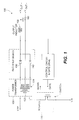
- the power processing circuit 100 includes a power train having a conversion stage including a switching circuit 110 for receiving input electrical power V IN and producing therefrom switched electrical power.
- the power processing circuit 100 further includes a filter circuit (including an output inductor 150 and output capacitor 160) for filtering the switched electrical power to produce output electrical power (represented as a voltage V OUT ).
- the power processing circuit 100 still further includes a power micromagnetic integrated circuit (e.g., transformer) 120, having a primary winding 123 and a secondary winding 126, and a rectifier (including rectifying diodes 130, 140) coupled between the power conversion stage and the filter stage.
- the transformer 120 is constructed according to the principles of the present invention as hereinafter described.
- the transformer 120 and power processing circuit 100 are submitted for illustrative purposes only and other power micromagnetic integrated circuits and applications therefor are well within the broad scope of the present invention.
- the power micromagnetic device 200 is an EE-type transformer device.
- the power micromagnetic device 200 includes a ferromagnetic core having a first core-portion 210 and a second core-portion 220. While the ferromagnetic core may be composed of an alloy [ e.g., a permalloyTM composed of nickel-iron including about 80% nickel and 20% iron), other ferromagnetic materials are well within the broad scope of the present invention.
- the power micromagnetic device 200 also includes conductive windings having a primary winding 230 and a secondary winding 240. Of course, the windings may be formed from any conductive material.
- the primary winding 230 terminates in a plurality of terminals 250, 260; the secondary winding 240 terminates in a plurality of terminals 270, 280.
- the first and second core-portions 210, 220 surround the primary and secondary windings 230, 240.
- the magnetic flux of the power micromagnetic device 200 predominantly flows along the width of the ferromagnetic core.
- the ferromagnetic core is anisotropic thereby controlling hysteresis losses at higher frequencies ( e.g., above 10 MHZ).
- the anisotropic property may be introduced by a deposition process in a uniform magnetic field through an energized solenoid or permanent magnet at levels of 10-500 Oersteds [("Oe"); 8000 - 40000 A/m].
- the induced anisotropy also produces a hard and easy axis, along which the permeability is a minimum and maximum.
- the permeability is increased five-fold from the hard axis to the easy axis as a result of the anistropy.
- the EE-type structure effectively controls the permeability of the ferromagnetic core by regulating the direction of the induced anisotropy with respect to the magnetic field vector.
- the first and second core-portion 230, 240 are coupled together by magnetic vias (when anisotropic characteristics and control are desired) or remain separate (when an air gap is desired).
- the total thickness thereof is selected based on the inductance requirements of the device.
- eddy currents induced in the ferromagnetic materials can become problematic due to the resulting low resistivity (e.g., ⁇ ⁇ 20-100 ⁇ cm).
- the film thickness should be below about 2 ⁇ m (obviously, thinner films are necessary as the permeability increases).
- insulated multiple layers of film should be employed.
- FIGURE 3 illustrated is a top view of another embodiment of a power micromagnetic device 300 constructed according to the principles of the present invention.
- the power micromagnetic device 300 is a toroidal transformer device.
- the power micromagnetic device 300 includes a ferromagnetic core 310 (proximate a window 325) and conductive windings (collectively designated 350) that surround the ferromagnetic core 310 through inner-layer connection vias (one of which as designated 375) and terminate in a plurality of terminals 380, 385, 390, 395.
- the inner-layer connection vias 375 lie within the window 310.
- the line space rules and distance between via requirements determine the size of the window 310.
- the dimension of the window 310 is limited as dictated by the thickness of the ferromagnetic material necessary to achieve the inductance characteristics.
- the inductance, as an example, for a toroidal device is maximized if the toroid is generally circular; the inductance is less if the toroid is formed into a square ( ⁇ 25% less) and finally degrades as the square is elongated into a rectangle.
- the size of the window 310 is determined by the minimum via size, via-via clearance and the number of vias (related to the number of primary and secondary turns). Therefore, to reduce the die size of the device, a larger core thicknesses is necessary to obtain an equivalent inductance to an EE ferromagnetic core of equal winding turns and core width.
- Toroidal transformers offer a relatively flat and smooth surface for the deposition of the ferromagnetic material thereby reducing the formation of stresses that may cause the degradation of the magnetic properties of the film deposited thereon. This is especially important when the ferromagnetic material has a high magnetostriction constant.
- the EE-type structure also, requires special provisions to create a continuous magnetic path from the first core-portion to the second core-portion. This is accomplished by introducing vias within the central core region and at the two outer core edges. The vias provide connectivity for the ferromagnetic material such that the first and second core-portions are coupled together continuously.
- the vias are a source of stress concentration that require additional slope reduction to decrease the accumulated stresses.
- FIGUREs illustrate both the EE-type and toroidal transformer device (including the advantages and disadvantages therefor), other power micromagnetic devices (including variations of the foregoing devices) and applications therefor are well within the broad scope of the present invention.
- FIGURE 4 illustrated is a cross-sectional view of an embodiment of a power micromagnetic integrated circuit (“PMIC") 400 constructed according to the principles of the present invention.
- the PMIC 400 includes a substrate (composed of, for instance, silicon, glass, ceramic or the like) 410 having a passivation layer (e.g., silicon-dioxide) 420 formed thereon using conventional formation processes such as a thermal growing process.
- the PMIC 400 further includes a first and second conductive winding layer (composed of, for instance, aluminum or any other conductive material) 440, 460 surrounded by first, second and third insulative layers or insulators 430, 450, 470.
- the PMIC 400 still further includes a metallic adhesive that contains a first adhesive layer (e.g., chromium) 480 and a second adhesive layer (e.g., silver) 485.
- the PMIC 400 still further includes a ferromagnetic core 490.
- the PMIC 400 still further includes a plurality of inner-layer vias (collectively designated 493) that provide multiple paths between layers of the PMIC 400 and a terminal 496 for connection to another device.
- the passivation layer 420 and first, second and third insulative layers 430, 450, 470 may be formed from an inorganic composition (e.g., silicon-dioxide, aluminum-dioxide, beryllium-dioxide), an organic polymer (e.g., a polyimide) or any other insulating material.
- an inorganic composition e.g., silicon-dioxide, aluminum-dioxide, beryllium-dioxide
- an organic polymer e.g., a polyimide
- the metallic adhesive is an inorganic-based material that is substantially (about 70%) free of titanium.
- first adhesive layer 480 generally contains materials selected from Group 4 elements (such as zirconium and hafnium; excluding about a 70% or more composition of titanium), Group 5 elements (such as vanadium, niobium and tantalum) and Group 6 elements (such as chromium, molybdenum and tungsten), other elements are well within the broad scope of the present invention. It should be noted that the above classifications of elements are compatible with the new Intemational Union of Pure and Applied Chemistry notation indicated in the periodic table. Additionally, while the second adhesive 485 generally contains metals such as gold, silver, platinum, palladium and copper, other materials susceptible to plating a ferromagnetic material are well within the broad scope of the present invention.
- Group 4 elements such as zirconium and hafnium; excluding about a 70% or more composition of titanium
- Group 5 elements such as vanadium, niobium and tantalum
- Group 6 elements such as chromium, molybdenum and tungsten
- the ferromagnetic core 490 may be composed of an alloy [such as the permalloyTM or a cobalt-iron composition), other ferromagnetic materials (e.g., an amorphous nickel phosphide) are well within the broad scope of the present invention.
- alloy such as the permalloyTM or a cobalt-iron composition
- other ferromagnetic materials e.g., an amorphous nickel phosphide
- a metallic adhesive that provides a secure interface to a ferromagnetic material and an insulator. For instance, when a metal such as sliver is exclusively used as the metallic adhesive, the ferromagnetic material/silver interface is stronger than the insulator/silver interface. As a result, the ferromagnetic material and silver films may be peeled away from the substrate at a specified testing peel force (using a standard adhesion evaluation technique for less than 1 kG/cm 2 ). Conversely, when chromium is exclusively used as the metallic adhesive, the insulator/chromium interface is stronger than the ferromagnetic material/chromium interface.
- the ferromagnetic material and silver films may be peeled away from the substrate at a specified testing peel force (using a standard adhesion evaluation technique for less than 1 kG/cm2).
- the chromium does not provide an adequate seed layer for plating the ferromagnetic material.
- the present invention therefore, introduces a metallic adhesive that provides an adequate bond between the ferromagnetic core 490 and the insulators 430, 450, 470 coupled to the substrate 410 to facilitate the fabrication of the PMIC 400.
- FIGURE 5 illustrated is a flow diagram of an embodiment of a method of manufacturing the PMIC of FIGURE 4.
- the method of manufacturing the PMIC is analogous to conventional silicon-on-silicon multi-chip-module processes [see Silicon-on-Silicon MCMs with Integrated Passive Components, by R.C. Frye, et al., Proc. 1992 IEEE Multi-Chip Module Conference, 155, Santa Cruz, Ca. (1992), which is herein incorporated by reference] with the following variations.
- a photolithographic process with photoresist is used to define the geometrical features of the PMIC based upon a 20 ⁇ m design rule.
- the photolithographic process generally includes the steps of exposing and developing the photoresist and etching away and stripping the unwanted portions of the material that the process is being applied to away from the circuit. Those skilled in the art should be familiar with conventional photolithographic processes.
- the PMIC employs a toroidal structure that includes multiple layers.
- the method begins at a start step 510.
- a silicon substrate is oxidized with a passivation layer an oxidize substrate step 520.
- the passivation layer is generally created using conventional thermal growing techniques or chemical vapor deposition techniques.
- the substrate may be blank or be composed of a pre-fabricated wafer with underlying circuitry and final passivation.
- the first conductive winding layer is, then, blanket deposited on the substrate during a deposit first conductive winding layer 530.
- the first conductive winding layer may be composed of aluminum that is sputter deposited (for instance, at 5 mtorr Argon pressure and room temperature) on the passivation layer having a thicknesses of about 2-10 ⁇ m.
- electroplated copper may be used to obtain thicknesses up to about 25 ⁇ m.
- the first conductive winding layer is then patterned to the desired configuration (including the desired contact regions for the PMIC) using a conventional photolithographic process. Of course, another contact region may be formed in the first conductive winding layer to facilitate electrical connectivity to other circuits coupled to the substrate.
- the first insulative layer is spin coated on the passivation layer and the first conductive winding layer during a deposit first insulative layer step 540.
- the first insulative layer is cured (at about 350°C for approximately 12 hours) and after shrinkage an insulative layer of about 3-5 ⁇ m thick is produced.
- the spin coating techniques generally, provide higher voltage isolation between the primary and secondary windings; generally, the voltage level breakdown values for isolation vary from 500 volts alternating current ("VAC") to 1500 VAC.
- VAC volts alternating current
- the first insulative layer is then patterned using a photolithographic process to form the inner-layer vias therethrough.
- the metallic adhesive including the first and second adhesive layers are blanket deposited on the first insulative layer during an apply metallic adhesive layer step 550.
- the first adhesive layer may be composed of chromium that is sputter deposited (for instance, at 5 mtorr Argon pressure and 250°C) on the first insulative layer having a thicknesses of about 250 A°.
- the second adhesive layer may be composed of silver that is sputter deposited (for instance, at 5 mtorr Argon pressure and room temperature) on the first adhesive layer having a thicknesses of about 500 A°.
- the metallic adhesive also serves as a seed layer for plating the ferromagnetic core.
- the ferromagnetic core is deposited ( e.g., electroplated in a thicknesses of about 2-12 ⁇ m) on the metallic adhesive during a deposit ferromagnetic core step 560.
- the ferromagnetic core may be plated in a buffered sulfamate bath under a controlled temperature ( e.g., 25-35°C) with a current density of about 30 mA/cm 2 .
- the metallic adhesive and ferromagnetic core are patterned to the desired configuration using a photolithographic process. With regard to the photolithographic process, the etching solutions should be capable of removing the unwanted metallic adhesive (e.g., chromium-silver composition) without attacking the deposited ferromagnetic film.
- a standard commercial cerric ammonium nitrate (“CAN") formulation etch solution etches the silver at the rate of about 50 A°/sec and the chromium at the rate of 250 A°/min without substantially affecting the ferromagnetic material.
- CAN cerric ammonium nitrate
- employing a CAN etch for approximately 60-75 seconds is adequate to pattern the metallic adhesive and ferromagnetic core.
- the first adhesive layer e.g., chromium
- the second adhesive layer e.g., silver
- the second adhesive layer may be composed of copper.
- a potassium iodide and water solution may be applied for about 10 seconds to perform the copper etching process and a potassium ferri-cyanide and potassium hydroxide solution may be applied for about 1-2 seconds to perform the chromium etching process.
- the potassium ferri-cyanide and potassium hydroxide solution does not substantially affect the copper layer underlying the ferromagnetic core thereby preventing the potential affects of undercutting.
- other types of etching processes (such as ion etching) are well within the broad scope of the present invention.
- the second insulative layer is spin coated on the ferromagnetic core and the first insulative layer during a deposit second insulative layer step 570.
- the second insulative layer is then patterned using a photolithographic process to form the inner-layer vias therethrough.
- the second conductive winding layer is, then, blanket deposited ( e.g., sputtered) on the second insulative layer during a deposit the second winding conductive layer step 580.
- the second conductive winding layer is then patterned to the desired configuration (including the desired contact regions) using a photolithographic process.
- the third insulative layer is spin coated on the second conductive winding layer and the second insulative layer during a deposit third insulative layer step 590.
- a terminal is finally formed in the third insulative layer during a form terminal step 599.
- the terminal is suitable for wire bonding (e.g., aluminum wire bonding) or is finished with a solder-wettable metal (e.g., chromium) for use with solder pastes for flip-chip assembly.
- the method terminates at an end step 599.
- a completed wafer may then be packaged as an integrated circuit or bare die mounted as in flip-chip assemblies.
- FIGUREs 4 and 5 illustrate an embodiment of a power micromagnetic integrated circuit and method of manufacture (including the photolithographic process) therefor, other power micromagnetic integrated circuits (including variations of the foregoing circuit) and methods of manufacture therefor are well within the broad scope of the present invention.
Landscapes
- Engineering & Computer Science (AREA)
- Power Engineering (AREA)
- Manufacturing & Machinery (AREA)
- Microelectronics & Electronic Packaging (AREA)
- Semiconductor Integrated Circuits (AREA)
- Coils Or Transformers For Communication (AREA)
- Hall/Mr Elements (AREA)
- Thin Magnetic Films (AREA)
Applications Claiming Priority (2)
| Application Number | Priority Date | Filing Date | Title |
|---|---|---|---|
| US872250 | 1997-06-10 | ||
| US08/872,250 US6118351A (en) | 1997-06-10 | 1997-06-10 | Micromagnetic device for power processing applications and method of manufacture therefor |
Publications (2)
| Publication Number | Publication Date |
|---|---|
| EP0884783A2 true EP0884783A2 (de) | 1998-12-16 |
| EP0884783A3 EP0884783A3 (de) | 1999-08-18 |
Family
ID=25359170
Family Applications (1)
| Application Number | Title | Priority Date | Filing Date |
|---|---|---|---|
| EP98304525A Withdrawn EP0884783A3 (de) | 1997-06-10 | 1998-06-09 | Mikromagnetische Vorrichtung zur Stromversorgung und ihr Herstellungsverfahren |
Country Status (8)
| Country | Link |
|---|---|
| US (4) | US6118351A (de) |
| EP (1) | EP0884783A3 (de) |
| JP (1) | JPH1174126A (de) |
| KR (1) | KR100305070B1 (de) |
| CN (1) | CN1203446A (de) |
| CA (1) | CA2237819C (de) |
| SG (1) | SG64491A1 (de) |
| TW (1) | TW373196B (de) |
Cited By (16)
| Publication number | Priority date | Publication date | Assignee | Title |
|---|---|---|---|---|
| EP1063661A1 (de) * | 1999-06-22 | 2000-12-27 | Lucent Technologies Inc. | Integrierte Schaltung mit einer mikromagnetischer Vorrichtung und sein Herstellungsverfahren |
| WO2002005076A3 (en) * | 2000-07-12 | 2002-05-10 | Sun Microsystems Inc | Powering ic chips using ac signals |
| WO2002071456A3 (en) * | 2001-01-19 | 2003-03-20 | Intel Corp | Magnetic layer processing |
| US6696744B2 (en) | 1997-06-10 | 2004-02-24 | Agere Systems, Inc. | Integrated circuit having a micromagnetic device and method of manufacture therefor |
| US6856228B2 (en) | 1999-11-23 | 2005-02-15 | Intel Corporation | Integrated inductor |
| US6856226B2 (en) | 1999-11-23 | 2005-02-15 | Intel Corporation | Integrated transformer |
| US6891461B2 (en) | 1999-11-23 | 2005-05-10 | Intel Corporation | Integrated transformer |
| US7327010B2 (en) | 1999-11-23 | 2008-02-05 | Intel Corporation | Inductors for integrated circuits |
| US7852185B2 (en) | 2003-05-05 | 2010-12-14 | Intel Corporation | On-die micro-transformer structures with magnetic materials |
| US7960269B2 (en) | 2005-07-22 | 2011-06-14 | Megica Corporation | Method for forming a double embossing structure |
| US7973629B2 (en) | 2001-09-04 | 2011-07-05 | Megica Corporation | Method for making high-performance RF integrated circuits |
| US8008775B2 (en) | 2004-09-09 | 2011-08-30 | Megica Corporation | Post passivation interconnection structures |
| US8018060B2 (en) | 2004-09-09 | 2011-09-13 | Megica Corporation | Post passivation interconnection process and structures |
| US8134548B2 (en) | 2005-06-30 | 2012-03-13 | Micron Technology, Inc. | DC-DC converter switching transistor current measurement technique |
| US8384189B2 (en) | 2005-03-29 | 2013-02-26 | Megica Corporation | High performance system-on-chip using post passivation process |
| US8487400B2 (en) | 1998-12-21 | 2013-07-16 | Megica Corporation | High performance system-on-chip using post passivation process |
Families Citing this family (111)
| Publication number | Priority date | Publication date | Assignee | Title |
|---|---|---|---|---|
| DE4442994A1 (de) * | 1994-12-02 | 1996-06-05 | Philips Patentverwaltung | Planare Induktivität |
| US6118351A (en) * | 1997-06-10 | 2000-09-12 | Lucent Technologies Inc. | Micromagnetic device for power processing applications and method of manufacture therefor |
| DE69930134T2 (de) * | 1998-09-17 | 2006-12-21 | Koninklijke Philips Electronics N.V. | Verfahren zur herstellung eines halbleiterkörpers auf dessen oberfläche sich eine spule mit magnetischem kern befindet |
| US8178435B2 (en) | 1998-12-21 | 2012-05-15 | Megica Corporation | High performance system-on-chip inductor using post passivation process |
| US8421158B2 (en) | 1998-12-21 | 2013-04-16 | Megica Corporation | Chip structure with a passive device and method for forming the same |
| US6563721B1 (en) * | 1999-11-10 | 2003-05-13 | Thomas & Betts International, Inc. | Power supply with multiple AC input voltages |
| US6342778B1 (en) * | 2000-04-20 | 2002-01-29 | Robert James Catalano | Low profile, surface mount magnetic devices |
| KR100403918B1 (ko) * | 2001-05-29 | 2003-10-30 | 타임스페이스시스템(주) | 음력날짜 표시시계 |
| KR100590525B1 (ko) * | 2003-01-15 | 2006-06-15 | 삼성전자주식회사 | 잉크젯 프린트헤드 및 잉크 토출 방법 |
| US8212317B2 (en) | 2004-01-29 | 2012-07-03 | Enpirion, Inc. | Integrated circuit with a laterally diffused metal oxide semiconductor device and method of forming the same |
| US8212316B2 (en) | 2004-01-29 | 2012-07-03 | Enpirion, Inc. | Integrated circuit with a laterally diffused metal oxide semiconductor device and method of forming the same |
| US8212315B2 (en) | 2004-01-29 | 2012-07-03 | Enpirion, Inc. | Integrated circuit with a laterally diffused metal oxide semiconductor device and method of forming the same |
| US8253195B2 (en) | 2004-01-29 | 2012-08-28 | Enpirion, Inc. | Integrated circuit with a laterally diffused metal oxide semiconductor device and method of forming the same |
| US7330017B2 (en) * | 2004-01-29 | 2008-02-12 | Enpirion, Inc. | Driver for a power converter and a method of driving a switch thereof |
| US7038438B2 (en) * | 2004-01-29 | 2006-05-02 | Enpirion, Inc. | Controller for a power converter and a method of controlling a switch thereof |
| US7230302B2 (en) * | 2004-01-29 | 2007-06-12 | Enpirion, Inc. | Laterally diffused metal oxide semiconductor device and method of forming the same |
| US8253196B2 (en) | 2004-01-29 | 2012-08-28 | Enpirion, Inc. | Integrated circuit with a laterally diffused metal oxide semiconductor device and method of forming the same |
| US8253197B2 (en) | 2004-01-29 | 2012-08-28 | Enpirion, Inc. | Integrated circuit with a laterally diffused metal oxide semiconductor device and method of forming the same |
| US7019505B2 (en) * | 2004-01-29 | 2006-03-28 | Enpirion, Inc. | Digital controller for a power converter employing selectable phases of a clock signal |
| US7015544B2 (en) | 2004-08-23 | 2006-03-21 | Enpirion, Inc. | Intergrated circuit employable with a power converter |
| US7214985B2 (en) * | 2004-08-23 | 2007-05-08 | Enpirion, Inc. | Integrated circuit incorporating higher voltage devices and low voltage devices therein |
| US7195981B2 (en) * | 2004-08-23 | 2007-03-27 | Enpirion, Inc. | Method of forming an integrated circuit employable with a power converter |
| US7229886B2 (en) * | 2004-08-23 | 2007-06-12 | Enpirion, Inc. | Method of forming an integrated circuit incorporating higher voltage devices and low voltage devices therein |
| US7335948B2 (en) * | 2004-08-23 | 2008-02-26 | Enpirion, Inc. | Integrated circuit incorporating higher voltage devices and low voltage devices therein |
| US7232733B2 (en) * | 2004-08-23 | 2007-06-19 | Enpirion, Inc. | Method of forming an integrated circuit incorporating higher voltage devices and low voltage devices therein |
| US7186606B2 (en) * | 2004-08-23 | 2007-03-06 | Enpirion, Inc. | Method of forming an integrated circuit employable with a power converter |
| US7190026B2 (en) * | 2004-08-23 | 2007-03-13 | Enpirion, Inc. | Integrated circuit employable with a power converter |
| US7276998B2 (en) * | 2004-11-10 | 2007-10-02 | Enpirion, Inc. | Encapsulated package for a magnetic device |
| US7462317B2 (en) * | 2004-11-10 | 2008-12-09 | Enpirion, Inc. | Method of manufacturing an encapsulated package for a magnetic device |
| US7180395B2 (en) * | 2004-11-10 | 2007-02-20 | Enpirion, Inc. | Encapsulated package for a magnetic device |
| US7426780B2 (en) | 2004-11-10 | 2008-09-23 | Enpirion, Inc. | Method of manufacturing a power module |
| US7256674B2 (en) * | 2004-11-10 | 2007-08-14 | Enpirion, Inc. | Power module |
| US8631560B2 (en) | 2005-10-05 | 2014-01-21 | Enpirion, Inc. | Method of forming a magnetic device having a conductive clip |
| US7688172B2 (en) | 2005-10-05 | 2010-03-30 | Enpirion, Inc. | Magnetic device having a conductive clip |
| US8701272B2 (en) | 2005-10-05 | 2014-04-22 | Enpirion, Inc. | Method of forming a power module with a magnetic device having a conductive clip |
| US8139362B2 (en) | 2005-10-05 | 2012-03-20 | Enpirion, Inc. | Power module with a magnetic device having a conductive clip |
| US7521907B2 (en) | 2006-03-06 | 2009-04-21 | Enpirion, Inc. | Controller for a power converter and method of operating the same |
| US7893676B2 (en) * | 2006-07-20 | 2011-02-22 | Enpirion, Inc. | Driver for switch and a method of driving the same |
| US7948280B2 (en) * | 2006-10-20 | 2011-05-24 | Enpirion, Inc. | Controller including a sawtooth generator and method of operating the same |
| US7675759B2 (en) | 2006-12-01 | 2010-03-09 | Flextronics International Usa, Inc. | Power system with power converters having an adaptive controller |
| US9197132B2 (en) | 2006-12-01 | 2015-11-24 | Flextronics International Usa, Inc. | Power converter with an adaptive controller and method of operating the same |
| US7468649B2 (en) | 2007-03-14 | 2008-12-23 | Flextronics International Usa, Inc. | Isolated power converter |
| JP5045219B2 (ja) * | 2007-04-27 | 2012-10-10 | 富士電機株式会社 | マイクロトランスの製造方法 |
| WO2008152641A2 (en) * | 2007-06-12 | 2008-12-18 | Advanced Magnetic Solutions Ltd. | Magnetic induction devices and methods for producing them |
| US8133529B2 (en) | 2007-09-10 | 2012-03-13 | Enpirion, Inc. | Method of forming a micromagnetic device |
| US7955868B2 (en) | 2007-09-10 | 2011-06-07 | Enpirion, Inc. | Method of forming a micromagnetic device |
| US7544995B2 (en) * | 2007-09-10 | 2009-06-09 | Enpirion, Inc. | Power converter employing a micromagnetic device |
| US7920042B2 (en) | 2007-09-10 | 2011-04-05 | Enpirion, Inc. | Micromagnetic device and method of forming the same |
| US8018315B2 (en) | 2007-09-10 | 2011-09-13 | Enpirion, Inc. | Power converter employing a micromagnetic device |
| US7952459B2 (en) * | 2007-09-10 | 2011-05-31 | Enpirion, Inc. | Micromagnetic device and method of forming the same |
| US7876080B2 (en) * | 2007-12-27 | 2011-01-25 | Enpirion, Inc. | Power converter with monotonic turn-on for pre-charged output capacitor |
| US7795700B2 (en) * | 2008-02-28 | 2010-09-14 | Broadcom Corporation | Inductively coupled integrated circuit with magnetic communication path and methods for use therewith |
| US8686698B2 (en) | 2008-04-16 | 2014-04-01 | Enpirion, Inc. | Power converter with controller operable in selected modes of operation |
| US8541991B2 (en) * | 2008-04-16 | 2013-09-24 | Enpirion, Inc. | Power converter with controller operable in selected modes of operation |
| US8410769B2 (en) * | 2008-04-16 | 2013-04-02 | Enpirion, Inc. | Power converter with controller operable in selected modes of operation |
| US8692532B2 (en) | 2008-04-16 | 2014-04-08 | Enpirion, Inc. | Power converter with controller operable in selected modes of operation |
| US9246390B2 (en) | 2008-04-16 | 2016-01-26 | Enpirion, Inc. | Power converter with controller operable in selected modes of operation |
| US7679342B2 (en) * | 2008-04-16 | 2010-03-16 | Enpirion, Inc. | Power converter with power switch operable in controlled current mode |
| US8339802B2 (en) | 2008-10-02 | 2012-12-25 | Enpirion, Inc. | Module having a stacked magnetic device and semiconductor device and method of forming the same |
| US8266793B2 (en) | 2008-10-02 | 2012-09-18 | Enpirion, Inc. | Module having a stacked magnetic device and semiconductor device and method of forming the same |
| US8153473B2 (en) | 2008-10-02 | 2012-04-10 | Empirion, Inc. | Module having a stacked passive element and method of forming the same |
| US9054086B2 (en) | 2008-10-02 | 2015-06-09 | Enpirion, Inc. | Module having a stacked passive element and method of forming the same |
| CN102217181B (zh) | 2008-11-14 | 2014-09-03 | 伟创力国际美国公司 | 用于同步整流器的驱动器以及采用该驱动器的功率转换器 |
| US9548714B2 (en) | 2008-12-29 | 2017-01-17 | Altera Corporation | Power converter with a dynamically configurable controller and output filter |
| US8698463B2 (en) | 2008-12-29 | 2014-04-15 | Enpirion, Inc. | Power converter with a dynamically configurable controller based on a power conversion mode |
| CN102342007B (zh) | 2009-01-19 | 2015-01-07 | 伟创力国际美国公司 | 用于功率转换器的控制器 |
| WO2010083514A1 (en) | 2009-01-19 | 2010-07-22 | Flextronics International Usa, Inc. | Controller for a power converter |
| US9019061B2 (en) | 2009-03-31 | 2015-04-28 | Power Systems Technologies, Ltd. | Magnetic device formed with U-shaped core pieces and power converter employing the same |
| US8643222B2 (en) | 2009-06-17 | 2014-02-04 | Power Systems Technologies Ltd | Power adapter employing a power reducer |
| US9077248B2 (en) | 2009-06-17 | 2015-07-07 | Power Systems Technologies Ltd | Start-up circuit for a power adapter |
| US8514593B2 (en) * | 2009-06-17 | 2013-08-20 | Power Systems Technologies, Ltd. | Power converter employing a variable switching frequency and a magnetic device with a non-uniform gap |
| US8638578B2 (en) | 2009-08-14 | 2014-01-28 | Power System Technologies, Ltd. | Power converter including a charge pump employable in a power adapter |
| US8976549B2 (en) | 2009-12-03 | 2015-03-10 | Power Systems Technologies, Ltd. | Startup circuit including first and second Schmitt triggers and power converter employing the same |
| US8520420B2 (en) | 2009-12-18 | 2013-08-27 | Power Systems Technologies, Ltd. | Controller for modifying dead time between switches in a power converter |
| US9246391B2 (en) | 2010-01-22 | 2016-01-26 | Power Systems Technologies Ltd. | Controller for providing a corrected signal to a sensed peak current through a circuit element of a power converter |
| US8787043B2 (en) | 2010-01-22 | 2014-07-22 | Power Systems Technologies, Ltd. | Controller for a power converter and method of operating the same |
| WO2011116225A1 (en) | 2010-03-17 | 2011-09-22 | Power Systems Technologies, Ltd. | Control system for a power converter and method of operating the same |
| US8130067B2 (en) * | 2010-05-11 | 2012-03-06 | Texas Instruments Incorporated | High frequency semiconductor transformer |
| US8867295B2 (en) | 2010-12-17 | 2014-10-21 | Enpirion, Inc. | Power converter for a memory module |
| US8792257B2 (en) | 2011-03-25 | 2014-07-29 | Power Systems Technologies, Ltd. | Power converter with reduced power dissipation |
| US8792256B2 (en) | 2012-01-27 | 2014-07-29 | Power Systems Technologies Ltd. | Controller for a switch and method of operating the same |
| US9190898B2 (en) | 2012-07-06 | 2015-11-17 | Power Systems Technologies, Ltd | Controller for a power converter and method of operating the same |
| US9214264B2 (en) | 2012-07-16 | 2015-12-15 | Power Systems Technologies, Ltd. | Magnetic device and power converter employing the same |
| US9106130B2 (en) | 2012-07-16 | 2015-08-11 | Power Systems Technologies, Inc. | Magnetic device and power converter employing the same |
| US9379629B2 (en) | 2012-07-16 | 2016-06-28 | Power Systems Technologies, Ltd. | Magnetic device and power converter employing the same |
| US9099232B2 (en) | 2012-07-16 | 2015-08-04 | Power Systems Technologies Ltd. | Magnetic device and power converter employing the same |
| US11058001B2 (en) | 2012-09-11 | 2021-07-06 | Ferric Inc. | Integrated circuit with laminated magnetic core inductor and magnetic flux closure layer |
| US9844141B2 (en) * | 2012-09-11 | 2017-12-12 | Ferric, Inc. | Magnetic core inductor integrated with multilevel wiring network |
| US10244633B2 (en) | 2012-09-11 | 2019-03-26 | Ferric Inc. | Integrated switched inductor power converter |
| US11064610B2 (en) | 2012-09-11 | 2021-07-13 | Ferric Inc. | Laminated magnetic core inductor with insulating and interface layers |
| US11197374B2 (en) | 2012-09-11 | 2021-12-07 | Ferric Inc. | Integrated switched inductor power converter having first and second powertrain phases |
| US11116081B2 (en) | 2012-09-11 | 2021-09-07 | Ferric Inc. | Laminated magnetic core inductor with magnetic flux closure path parallel to easy axes of magnetization of magnetic layers |
| US10893609B2 (en) | 2012-09-11 | 2021-01-12 | Ferric Inc. | Integrated circuit with laminated magnetic core inductor including a ferromagnetic alloy |
| US20140159130A1 (en) | 2012-11-30 | 2014-06-12 | Enpirion, Inc. | Apparatus including a semiconductor device coupled to a decoupling device |
| US9240712B2 (en) | 2012-12-13 | 2016-01-19 | Power Systems Technologies Ltd. | Controller including a common current-sense device for power switches of a power converter |
| US9300206B2 (en) | 2013-11-15 | 2016-03-29 | Power Systems Technologies Ltd. | Method for estimating power of a power converter |
| US10020739B2 (en) | 2014-03-27 | 2018-07-10 | Altera Corporation | Integrated current replicator and method of operating the same |
| US9536938B1 (en) | 2013-11-27 | 2017-01-03 | Altera Corporation | Semiconductor device including a resistor metallic layer and method of forming the same |
| US9673192B1 (en) | 2013-11-27 | 2017-06-06 | Altera Corporation | Semiconductor device including a resistor metallic layer and method of forming the same |
| US9647053B2 (en) | 2013-12-16 | 2017-05-09 | Ferric Inc. | Systems and methods for integrated multi-layer magnetic films |
| US10629357B2 (en) | 2014-06-23 | 2020-04-21 | Ferric Inc. | Apparatus and methods for magnetic core inductors with biased permeability |
| US11302469B2 (en) | 2014-06-23 | 2022-04-12 | Ferric Inc. | Method for fabricating inductors with deposition-induced magnetically-anisotropic cores |
| US10103627B2 (en) | 2015-02-26 | 2018-10-16 | Altera Corporation | Packaged integrated circuit including a switch-mode regulator and method of forming the same |
| US9509217B2 (en) | 2015-04-20 | 2016-11-29 | Altera Corporation | Asymmetric power flow controller for a power converter and method of operating the same |
| JP6582183B2 (ja) * | 2015-09-03 | 2019-10-02 | ローム株式会社 | 磁気デバイス、およびパワーモジュール |
| US20180061569A1 (en) * | 2016-08-26 | 2018-03-01 | Analog Devices Global | Methods of manufacture of an inductive component and an inductive component |
| DE102018113765B4 (de) | 2017-06-09 | 2023-11-02 | Analog Devices International Unlimited Company | Transformator mit einer durchkontaktierung für einen magnetkern |
| US10892230B2 (en) * | 2018-07-30 | 2021-01-12 | Taiwan Semiconductor Manufacturing Co., Ltd. | Magnetic shielding material with insulator-coated ferromagnetic particles |
| US12322695B2 (en) | 2020-12-01 | 2025-06-03 | Ferric Inc. | Magnetic core with hard ferromagnetic biasing layers and structures containing same |
| CN112967879B (zh) * | 2021-02-01 | 2022-12-06 | 新昌县新明实业有限公司 | 一种变压器绝缘材料电瓷成型加工工艺 |
| US12125713B2 (en) | 2022-03-22 | 2024-10-22 | Ferric Inc. | Method for manufacturing ferromagnetic-dielectric composite material |
Family Cites Families (31)
| Publication number | Priority date | Publication date | Assignee | Title |
|---|---|---|---|---|
| GB1374626A (en) * | 1970-10-30 | 1974-11-20 | Matsushita Electronics Corp | Method of making a semiconductor device |
| US3873944A (en) * | 1973-03-01 | 1975-03-25 | Varian Associates | Bonding of ferrite to metal for high-power microwave applications |
| US4016050A (en) * | 1975-05-12 | 1977-04-05 | Bell Telephone Laboratories, Incorporated | Conduction system for thin film and hybrid integrated circuits |
| US4740657A (en) * | 1986-02-14 | 1988-04-26 | Hitachi, Chemical Company, Ltd | Anisotropic-electroconductive adhesive composition, method for connecting circuits using the same, and connected circuit structure thus obtained |
| JP2559700B2 (ja) * | 1986-03-18 | 1996-12-04 | 富士通株式会社 | 半導体装置の製造方法 |
| JPS6453324A (en) * | 1987-08-24 | 1989-03-01 | Matsushita Electric Industrial Co Ltd | Magnetic recording medium |
| US4939610A (en) * | 1987-10-05 | 1990-07-03 | Hitachi, Ltd. | Thin film magnetic head having magnetic core including a thin film of cobalt alloy |
| JP2501873B2 (ja) * | 1988-06-23 | 1996-05-29 | シャープ株式会社 | 薄膜磁気ヘッドの製造方法 |
| US4853080A (en) * | 1988-12-14 | 1989-08-01 | Hewlett-Packard | Lift-off process for patterning shields in thin magnetic recording heads |
| US5037517A (en) * | 1989-02-17 | 1991-08-06 | Vac-Tec Systems, Inc. | Method of forming layered structure for adhering gold to a substrate |
| US5276763A (en) * | 1990-07-09 | 1994-01-04 | Heraeus Quarzglas Gmbh | Infrared radiator with protected reflective coating and method for manufacturing same |
| EP0575280A3 (en) * | 1992-06-18 | 1995-10-04 | Ibm | Cmos transistor with two-layer inverse-t tungsten gate structure |
| US5312674A (en) * | 1992-07-31 | 1994-05-17 | Hughes Aircraft Company | Low-temperature-cofired-ceramic (LTCC) tape structures including cofired ferromagnetic elements, drop-in components and multi-layer transformer |
| US5587130A (en) * | 1993-03-15 | 1996-12-24 | Arizona Board Of Regents | Selected area adhesion and surface passivation of metal films |
| US5525941A (en) * | 1993-04-01 | 1996-06-11 | General Electric Company | Magnetic and electromagnetic circuit components having embedded magnetic material in a high density interconnect structure |
| US5667884A (en) * | 1993-04-12 | 1997-09-16 | Bolger; Justin C. | Area bonding conductive adhesive preforms |
| JPH0766033A (ja) * | 1993-08-30 | 1995-03-10 | Mitsubishi Electric Corp | 磁気抵抗素子ならびにその磁気抵抗素子を用いた磁性薄膜メモリおよび磁気抵抗センサ |
| KR950012334A (ko) * | 1993-10-29 | 1995-05-16 | 윌리엄 티. 엘리스 | 자기 저항 헤드 어셈블리 및 자기 저항 헤드를 정전하 방전으로부터 보호하는 방법 |
| US5512818A (en) * | 1994-03-31 | 1996-04-30 | At&T Corp. | Voltage proportional replication device using magnetoresistive sensing elements |
| EP0681319B1 (de) * | 1994-04-15 | 2002-10-30 | Kabushiki Kaisha Toshiba | Halbleiterbauteil und Verfahren zur Herstellung desselben |
| EP0689214B1 (de) * | 1994-06-21 | 1999-09-22 | Sumitomo Special Metals Co., Ltd. | Herstellungsverfahren für Substrat mit mehrschichtigen gedruckten Spulen |
| US5631509A (en) * | 1994-07-27 | 1997-05-20 | General Electric Company | Motor having thermostatically controlled or limited space heater |
| CN1096119C (zh) * | 1994-10-06 | 2002-12-11 | 钟渊化学工业株式会社 | 薄膜太阳能电池 |
| US5635892A (en) * | 1994-12-06 | 1997-06-03 | Lucent Technologies Inc. | High Q integrated inductor |
| JP3549294B2 (ja) * | 1995-08-23 | 2004-08-04 | 新光電気工業株式会社 | 半導体装置及びその実装構造 |
| DE19606101A1 (de) * | 1996-02-19 | 1997-08-21 | Siemens Ag | Halbleiterkörper mit Lotmaterialschicht |
| US5659462A (en) * | 1996-04-12 | 1997-08-19 | Lucent Technologies Inc. | Encapsulated, integrated power magnetic device and method of manufacture therefor |
| US6057237A (en) * | 1997-04-29 | 2000-05-02 | Applied Materials, Inc. | Tantalum-containing barrier layers for copper |
| US6118351A (en) * | 1997-06-10 | 2000-09-12 | Lucent Technologies Inc. | Micromagnetic device for power processing applications and method of manufacture therefor |
| US5925827A (en) * | 1997-09-25 | 1999-07-20 | Lucent Technologies Inc. | System and method for empirically determining shrinkage stresses in a molded package and power module employing the same |
| US6055179A (en) * | 1998-05-19 | 2000-04-25 | Canon Kk | Memory device utilizing giant magnetoresistance effect |
-
1997
- 1997-06-10 US US08/872,250 patent/US6118351A/en not_active Expired - Lifetime
-
1998
- 1998-05-15 TW TW087107558A patent/TW373196B/zh active
- 1998-05-19 CA CA002237819A patent/CA2237819C/en not_active Expired - Fee Related
- 1998-06-08 SG SG1998001313A patent/SG64491A1/en unknown
- 1998-06-09 EP EP98304525A patent/EP0884783A3/de not_active Withdrawn
- 1998-06-09 CN CN98109818A patent/CN1203446A/zh active Pending
- 1998-06-10 JP JP10162523A patent/JPH1174126A/ja active Pending
- 1998-06-10 KR KR1019980021475A patent/KR100305070B1/ko not_active Expired - Fee Related
- 1998-07-02 US US09/109,963 patent/US6163234A/en not_active Expired - Lifetime
-
2000
- 2000-01-24 US US09/490,655 patent/US6160721A/en not_active Expired - Lifetime
-
2003
- 2003-03-13 US US10/387,846 patent/US7021518B2/en not_active Expired - Fee Related
Cited By (35)
| Publication number | Priority date | Publication date | Assignee | Title |
|---|---|---|---|---|
| US6696744B2 (en) | 1997-06-10 | 2004-02-24 | Agere Systems, Inc. | Integrated circuit having a micromagnetic device and method of manufacture therefor |
| US8487400B2 (en) | 1998-12-21 | 2013-07-16 | Megica Corporation | High performance system-on-chip using post passivation process |
| US6649422B2 (en) | 1999-06-22 | 2003-11-18 | Agere Systems Inc. | Integrated circuit having a micromagnetic device and method of manufacture therefor |
| US6255714B1 (en) | 1999-06-22 | 2001-07-03 | Agere Systems Guardian Corporation | Integrated circuit having a micromagnetic device including a ferromagnetic core and method of manufacture therefor |
| EP1063661A1 (de) * | 1999-06-22 | 2000-12-27 | Lucent Technologies Inc. | Integrierte Schaltung mit einer mikromagnetischer Vorrichtung und sein Herstellungsverfahren |
| US7119650B2 (en) | 1999-11-23 | 2006-10-10 | Intel Corporation | Integrated transformer |
| US7434306B2 (en) | 1999-11-23 | 2008-10-14 | Intel Corporation | Integrated transformer |
| US6815220B2 (en) | 1999-11-23 | 2004-11-09 | Intel Corporation | Magnetic layer processing |
| US6856228B2 (en) | 1999-11-23 | 2005-02-15 | Intel Corporation | Integrated inductor |
| US6856226B2 (en) | 1999-11-23 | 2005-02-15 | Intel Corporation | Integrated transformer |
| US6870456B2 (en) | 1999-11-23 | 2005-03-22 | Intel Corporation | Integrated transformer |
| US6891461B2 (en) | 1999-11-23 | 2005-05-10 | Intel Corporation | Integrated transformer |
| US6940147B2 (en) | 1999-11-23 | 2005-09-06 | Intel Corporation | Integrated inductor having magnetic layer |
| US6943658B2 (en) | 1999-11-23 | 2005-09-13 | Intel Corporation | Integrated transformer |
| US6988307B2 (en) | 1999-11-23 | 2006-01-24 | Intel Corporation | Method of making an integrated inductor |
| US7064646B2 (en) | 1999-11-23 | 2006-06-20 | Intel Corporation | Integrated inductor |
| US7982574B2 (en) | 1999-11-23 | 2011-07-19 | Intel Corporation | Integrated transformer |
| US7299537B2 (en) | 1999-11-23 | 2007-11-27 | Intel Corporation | Method of making an integrated inductor |
| US7327010B2 (en) | 1999-11-23 | 2008-02-05 | Intel Corporation | Inductors for integrated circuits |
| US7332792B2 (en) | 1999-11-23 | 2008-02-19 | Intel Corporation | Magnetic layer processing |
| US7791447B2 (en) | 1999-11-23 | 2010-09-07 | Intel Corporation | Integrated transformer |
| WO2002005076A3 (en) * | 2000-07-12 | 2002-05-10 | Sun Microsystems Inc | Powering ic chips using ac signals |
| US6597593B1 (en) | 2000-07-12 | 2003-07-22 | Sun Microsystems, Inc. | Powering IC chips using AC signals |
| WO2002071456A3 (en) * | 2001-01-19 | 2003-03-20 | Intel Corp | Magnetic layer processing |
| US8384508B2 (en) | 2001-09-04 | 2013-02-26 | Megica Corporation | Method for making high-performance RF integrated circuits |
| US7973629B2 (en) | 2001-09-04 | 2011-07-05 | Megica Corporation | Method for making high-performance RF integrated circuits |
| US8471667B2 (en) | 2003-05-05 | 2013-06-25 | Intel Corporation | On-die micro-transformer structures with magnetic materials |
| US7852185B2 (en) | 2003-05-05 | 2010-12-14 | Intel Corporation | On-die micro-transformer structures with magnetic materials |
| US8008775B2 (en) | 2004-09-09 | 2011-08-30 | Megica Corporation | Post passivation interconnection structures |
| US8018060B2 (en) | 2004-09-09 | 2011-09-13 | Megica Corporation | Post passivation interconnection process and structures |
| US8384189B2 (en) | 2005-03-29 | 2013-02-26 | Megica Corporation | High performance system-on-chip using post passivation process |
| US8134548B2 (en) | 2005-06-30 | 2012-03-13 | Micron Technology, Inc. | DC-DC converter switching transistor current measurement technique |
| US8482552B2 (en) | 2005-06-30 | 2013-07-09 | Micron Technology, Inc. | DC-DC converter switching transistor current measurement technique |
| US9124174B2 (en) | 2005-06-30 | 2015-09-01 | Micron Technology, Inc. | DC-DC converter switching transistor current measurement technique |
| US7960269B2 (en) | 2005-07-22 | 2011-06-14 | Megica Corporation | Method for forming a double embossing structure |
Also Published As
| Publication number | Publication date |
|---|---|
| TW373196B (en) | 1999-11-01 |
| US20030150898A1 (en) | 2003-08-14 |
| US6118351A (en) | 2000-09-12 |
| SG64491A1 (en) | 1999-04-27 |
| EP0884783A3 (de) | 1999-08-18 |
| US6160721A (en) | 2000-12-12 |
| KR19990006843A (ko) | 1999-01-25 |
| CA2237819A1 (en) | 1998-12-10 |
| US7021518B2 (en) | 2006-04-04 |
| KR100305070B1 (ko) | 2001-11-02 |
| US6163234A (en) | 2000-12-19 |
| JPH1174126A (ja) | 1999-03-16 |
| CN1203446A (zh) | 1998-12-30 |
| CA2237819C (en) | 2001-02-13 |
Similar Documents
| Publication | Publication Date | Title |
|---|---|---|
| US6118351A (en) | Micromagnetic device for power processing applications and method of manufacture therefor | |
| EP1063661B1 (de) | Integrierte Schaltung mit einer mikromagnetischer Vorrichtung und sein Herstellungsverfahren | |
| US6696744B2 (en) | Integrated circuit having a micromagnetic device and method of manufacture therefor | |
| US7791447B2 (en) | Integrated transformer | |
| US6191495B1 (en) | Micromagnetic device having an anisotropic ferromagnetic core and method of manufacture therefor | |
| US6870456B2 (en) | Integrated transformer | |
| US7119650B2 (en) | Integrated transformer | |
| US6459352B1 (en) | On-chip transformers | |
| US6992871B2 (en) | Microtransformer for system-on-chip power supply | |
| US6738240B1 (en) | Microtransformer for system-on-chip power supply | |
| US8531002B2 (en) | Apparatus and method for wafer level fabrication of high value inductors on semiconductor integrated circuits | |
| US6420954B1 (en) | Coupled multilayer soft magnetic films for high frequency microtransformer for system-on-chip power supply | |
| JPH05109557A (ja) | 高周波用薄膜トランスおよび高周波用薄膜インダクタ | |
| JP3544758B2 (ja) | 電子部品および磁気部品 | |
| CN117153520A (zh) | 电感器 |
Legal Events
| Date | Code | Title | Description |
|---|---|---|---|
| PUAI | Public reference made under article 153(3) epc to a published international application that has entered the european phase |
Free format text: ORIGINAL CODE: 0009012 |
|
| AK | Designated contracting states |
Kind code of ref document: A2 Designated state(s): DE ES FR GB |
|
| AX | Request for extension of the european patent |
Free format text: AL;LT;LV;MK;RO;SI |
|
| PUAL | Search report despatched |
Free format text: ORIGINAL CODE: 0009013 |
|
| AK | Designated contracting states |
Kind code of ref document: A3 Designated state(s): AT BE CH CY DE DK ES FI FR GB GR IE IT LI LU MC NL PT SE |
|
| AX | Request for extension of the european patent |
Free format text: AL;LT;LV;MK;RO;SI |
|
| RIC1 | Information provided on ipc code assigned before grant |
Free format text: 6H 01L 27/01 A, 6H 01F 17/00 B, 6H 01F 41/04 B |
|
| 17P | Request for examination filed |
Effective date: 20000207 |
|
| AKX | Designation fees paid |
Free format text: DE ES FR GB |
|
| STAA | Information on the status of an ep patent application or granted ep patent |
Free format text: STATUS: THE APPLICATION IS DEEMED TO BE WITHDRAWN |
|
| 18D | Application deemed to be withdrawn |
Effective date: 20030102 |