EP0886144B1 - Capteur scellé hermétiquement avec microstructure mobile - Google Patents
Capteur scellé hermétiquement avec microstructure mobile Download PDFInfo
- Publication number
- EP0886144B1 EP0886144B1 EP97830290A EP97830290A EP0886144B1 EP 0886144 B1 EP0886144 B1 EP 0886144B1 EP 97830290 A EP97830290 A EP 97830290A EP 97830290 A EP97830290 A EP 97830290A EP 0886144 B1 EP0886144 B1 EP 0886144B1
- Authority
- EP
- European Patent Office
- Prior art keywords
- chip
- sensor
- sensitive element
- electrical signal
- wafer
- Prior art date
- Legal status (The legal status is an assumption and is not a legal conclusion. Google has not performed a legal analysis and makes no representation as to the accuracy of the status listed.)
- Expired - Lifetime
Links
- 238000000034 method Methods 0.000 claims description 28
- 229910052751 metal Inorganic materials 0.000 claims description 22
- 239000002184 metal Substances 0.000 claims description 22
- 239000004065 semiconductor Substances 0.000 claims description 16
- 239000000463 material Substances 0.000 claims description 13
- PXHVJJICTQNCMI-UHFFFAOYSA-N Nickel Chemical compound [Ni] PXHVJJICTQNCMI-UHFFFAOYSA-N 0.000 claims description 8
- 238000005520 cutting process Methods 0.000 claims description 4
- 229910052759 nickel Inorganic materials 0.000 claims description 4
- 239000004033 plastic Substances 0.000 claims description 4
- 229920003023 plastic Polymers 0.000 claims description 4
- 238000003466 welding Methods 0.000 claims description 4
- 230000001419 dependent effect Effects 0.000 claims description 3
- FGUUSXIOTUKUDN-IBGZPJMESA-N C1(=CC=CC=C1)N1C2=C(NC([C@H](C1)NC=1OC(=NN=1)C1=CC=CC=C1)=O)C=CC=C2 Chemical compound C1(=CC=CC=C1)N1C2=C(NC([C@H](C1)NC=1OC(=NN=1)C1=CC=CC=C1)=O)C=CC=C2 FGUUSXIOTUKUDN-IBGZPJMESA-N 0.000 claims 1
- 235000012431 wafers Nutrition 0.000 description 15
- XUIMIQQOPSSXEZ-UHFFFAOYSA-N Silicon Chemical compound [Si] XUIMIQQOPSSXEZ-UHFFFAOYSA-N 0.000 description 4
- 229910052710 silicon Inorganic materials 0.000 description 4
- 239000010703 silicon Substances 0.000 description 4
- 239000004411 aluminium Substances 0.000 description 3
- 229910052782 aluminium Inorganic materials 0.000 description 3
- XAGFODPZIPBFFR-UHFFFAOYSA-N aluminium Chemical compound [Al] XAGFODPZIPBFFR-UHFFFAOYSA-N 0.000 description 3
- 239000012467 final product Substances 0.000 description 3
- PCHJSUWPFVWCPO-UHFFFAOYSA-N gold Chemical compound [Au] PCHJSUWPFVWCPO-UHFFFAOYSA-N 0.000 description 3
- 229910052737 gold Inorganic materials 0.000 description 3
- 239000010931 gold Substances 0.000 description 3
- 238000004519 manufacturing process Methods 0.000 description 3
- 238000005459 micromachining Methods 0.000 description 3
- IJGRMHOSHXDMSA-UHFFFAOYSA-N Atomic nitrogen Chemical compound N#N IJGRMHOSHXDMSA-UHFFFAOYSA-N 0.000 description 2
- RYGMFSIKBFXOCR-UHFFFAOYSA-N Copper Chemical compound [Cu] RYGMFSIKBFXOCR-UHFFFAOYSA-N 0.000 description 2
- VYPSYNLAJGMNEJ-UHFFFAOYSA-N Silicium dioxide Chemical compound O=[Si]=O VYPSYNLAJGMNEJ-UHFFFAOYSA-N 0.000 description 2
- 230000001133 acceleration Effects 0.000 description 2
- 239000000853 adhesive Substances 0.000 description 2
- 230000001070 adhesive effect Effects 0.000 description 2
- 239000000956 alloy Substances 0.000 description 2
- 229910045601 alloy Inorganic materials 0.000 description 2
- 230000015572 biosynthetic process Effects 0.000 description 2
- 239000003990 capacitor Substances 0.000 description 2
- 238000001816 cooling Methods 0.000 description 2
- 229910052802 copper Inorganic materials 0.000 description 2
- 239000010949 copper Substances 0.000 description 2
- 238000013016 damping Methods 0.000 description 2
- 238000001035 drying Methods 0.000 description 2
- 239000011521 glass Substances 0.000 description 2
- 238000002844 melting Methods 0.000 description 2
- 230000008018 melting Effects 0.000 description 2
- 230000003647 oxidation Effects 0.000 description 2
- 238000007254 oxidation reaction Methods 0.000 description 2
- XLYOFNOQVPJJNP-UHFFFAOYSA-N water Substances O XLYOFNOQVPJJNP-UHFFFAOYSA-N 0.000 description 2
- HCHKCACWOHOZIP-UHFFFAOYSA-N Zinc Chemical compound [Zn] HCHKCACWOHOZIP-UHFFFAOYSA-N 0.000 description 1
- 238000004026 adhesive bonding Methods 0.000 description 1
- 239000000919 ceramic Substances 0.000 description 1
- 238000007906 compression Methods 0.000 description 1
- 238000009792 diffusion process Methods 0.000 description 1
- 238000004070 electrodeposition Methods 0.000 description 1
- 238000009713 electroplating Methods 0.000 description 1
- 238000005538 encapsulation Methods 0.000 description 1
- 230000007613 environmental effect Effects 0.000 description 1
- 239000003822 epoxy resin Substances 0.000 description 1
- 238000005530 etching Methods 0.000 description 1
- 238000001704 evaporation Methods 0.000 description 1
- 230000008020 evaporation Effects 0.000 description 1
- -1 for example Substances 0.000 description 1
- 239000007789 gas Substances 0.000 description 1
- XLYOFNOQVPJJNP-UHFFFAOYSA-M hydroxide Chemical compound [OH-] XLYOFNOQVPJJNP-UHFFFAOYSA-M 0.000 description 1
- 230000010354 integration Effects 0.000 description 1
- 230000002452 interceptive effect Effects 0.000 description 1
- 238000002955 isolation Methods 0.000 description 1
- 238000005304 joining Methods 0.000 description 1
- LQBJWKCYZGMFEV-UHFFFAOYSA-N lead tin Chemical compound [Sn].[Pb] LQBJWKCYZGMFEV-UHFFFAOYSA-N 0.000 description 1
- 239000007788 liquid Substances 0.000 description 1
- 238000003754 machining Methods 0.000 description 1
- 230000000873 masking effect Effects 0.000 description 1
- 238000012986 modification Methods 0.000 description 1
- 230000004048 modification Effects 0.000 description 1
- 238000012544 monitoring process Methods 0.000 description 1
- 229910052757 nitrogen Inorganic materials 0.000 description 1
- 229910000510 noble metal Inorganic materials 0.000 description 1
- 239000002245 particle Substances 0.000 description 1
- 229920000647 polyepoxide Polymers 0.000 description 1
- 238000006116 polymerization reaction Methods 0.000 description 1
- 230000001105 regulatory effect Effects 0.000 description 1
- 229920005989 resin Polymers 0.000 description 1
- 239000011347 resin Substances 0.000 description 1
- 239000000565 sealant Substances 0.000 description 1
- 230000035945 sensitivity Effects 0.000 description 1
- 235000012239 silicon dioxide Nutrition 0.000 description 1
- 239000000377 silicon dioxide Substances 0.000 description 1
- 229910000679 solder Inorganic materials 0.000 description 1
- 238000005476 soldering Methods 0.000 description 1
- 239000000126 substance Substances 0.000 description 1
- 239000000725 suspension Substances 0.000 description 1
- 229920001187 thermosetting polymer Polymers 0.000 description 1
- 238000002604 ultrasonography Methods 0.000 description 1
- 229910052725 zinc Inorganic materials 0.000 description 1
- 239000011701 zinc Substances 0.000 description 1
Images
Classifications
-
- B—PERFORMING OPERATIONS; TRANSPORTING
- B81—MICROSTRUCTURAL TECHNOLOGY
- B81C—PROCESSES OR APPARATUS SPECIALLY ADAPTED FOR THE MANUFACTURE OR TREATMENT OF MICROSTRUCTURAL DEVICES OR SYSTEMS
- B81C1/00—Manufacture or treatment of devices or systems in or on a substrate
- B81C1/00015—Manufacture or treatment of devices or systems in or on a substrate for manufacturing microsystems
- B81C1/00222—Integrating an electronic processing unit with a micromechanical structure
- B81C1/0023—Packaging together an electronic processing unit die and a micromechanical structure die
-
- G—PHYSICS
- G01—MEASURING; TESTING
- G01P—MEASURING LINEAR OR ANGULAR SPEED, ACCELERATION, DECELERATION, OR SHOCK; INDICATING PRESENCE, ABSENCE, OR DIRECTION, OF MOVEMENT
- G01P1/00—Details of instruments
- G01P1/02—Housings
-
- G—PHYSICS
- G01—MEASURING; TESTING
- G01P—MEASURING LINEAR OR ANGULAR SPEED, ACCELERATION, DECELERATION, OR SHOCK; INDICATING PRESENCE, ABSENCE, OR DIRECTION, OF MOVEMENT
- G01P15/00—Measuring acceleration; Measuring deceleration; Measuring shock, i.e. sudden change of acceleration
- G01P15/02—Measuring acceleration; Measuring deceleration; Measuring shock, i.e. sudden change of acceleration by making use of inertia forces using solid seismic masses
- G01P15/08—Measuring acceleration; Measuring deceleration; Measuring shock, i.e. sudden change of acceleration by making use of inertia forces using solid seismic masses with conversion into electric or magnetic values
- G01P15/0802—Details
Definitions
- the present invention relates to a sensor with a movable microstructure and, in particular, to a sensor according to the preamble of the first claim.
- Sensors with movable microstructures such as, for example, inertial sensors which can measure a physical quantity relating to a movement of the sensor and produce an output signal dependent on the quantity are used in various applications, for example, in the automotive field for monitoring various devices such as air bags, anti-slip braking systems (ABS), and active suspensions, or in other fields such as consumer electronics, computers and the like.
- Sensors with movable microstructures are formed on a microscopic scale in chips of semiconductor material; a sensor of this type comprises a sensitive element which can produce an electrical signal relating to the movement of a microstructure movable relative to a surface of the chip.
- the sensitive element In sensors with movable microstructures, the sensitive element has to be suitably protected by being enclosed in a hermetic structure to ensure that it operates in a controlled environment; this allows the microstructure of the sensitive element, which has a very small mass, to move with little resistance and minimal damping so as to ensure good sensitivity of the sensor.
- a sensor of this type also includes a circuitry which processes the electrical signal generated by the sensitive element and which, in turn, has to be encapsulated in a suitable container (package) which protects the processing circuit from external environmental conditions, ensuring that it operates correctly.
- a known technique for protecting a sensor with a movable microstructure consists in the encapsulation of the sensitive element and the processing circuitry in a hermetic, for example, ceramic or metal package; the sensitive element and the processing circuitry can thus be incorporated in the same semiconductor chip.
- this technique is extremely expensive, resulting in a high final product cost.
- a different known technique consists in the production of a hollow structure on a microscopic scale (a micro-cavity) which houses the sensitive element.
- This isolation method involves micromachining of a silicon or glass chip which is then connected to the chip on which the sensitive element is formed, for example, by an anodic bonding technique; this technique allows inexpensive standard plastics packages to be used for encapsulating the final product.
- the known solution described above is quite complex and expensive.
- this technique does not allow the sensitive element and the processing circuitry to be incorporated in the same chip since the bonding step requires the surfaces to be joined to be perfectly flat (with a peak-valley roughness of the order of a hundred ⁇ ); generally, the plate containing the sensitive element and that containing the processing circuitry are arranged side by side and are connected electrically by means of suitable metal wires.
- the sensitive elements of sensors with movable microstructures are usually made in large numbers in several identical areas of a wafer of semiconductor material which are subsequently separated by a suitable cutting operation.
- the cutting is generally carried out by means of a high-velocity, water-cooled, diamond-blade saw.
- a further disadvantage of the known sensors is that, during the drying of the water used for cooling the blade, permanent sticking or "stiction" of the movable high-velocity, water-cooled, diamond-blade saw.
- a further disadvantage of the known sensors is that, during the drying of the water used for cooling the blade, permanent sticking or "stiction" of the movable microstructure to an underlying surface of the semiconductor chip may occur. This physical phenomenon renders the sensor unusable.
- Document US-5164328 discloses a method of joining an integrated circuit die and a sensor die by the use of solder bumps for the formation of a hybrid circuit assembly. According to this document a dielectric sealant is deposited around the outside edges of the sensor to prevent foreign material such as encapsulating material from interfering with the operation of the sensor.
- Document EP-773443-A1 describes micromechanical acceleration sensor consisting of two semiconductor wafers and having a cavity housing movable electrodes. This cavity is provided with lateral walls made by silicon layers overlapped to metal layers.
- the object of the present invention is to prevent the aforementioned drawbacks.
- a sensor with a movable microstructure as described in the first claim is proposed.
- the sensor with a movable microstructure according to the present invention is particularly compact, simple and inexpensive.
- This sensor permits the optional use of a plastics, and hence extremely inexpensive, package for encapsulating the final product.
- the method of producing the sensor of the present invention does not require micromachining of a further silicon or glass wafer or connection thereof to the wafer on which the sensitive elements are formed. Moreover, both of the semiconductor chips used in the structure of the present invention contain active elements (the sensitive element and the processing circuitry, respectively) so that there is no wastage of material.
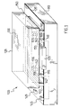
- the drawing shows a sensor 100 having a movable microstructure and constituted, in particular, by an inertial sensor comprising a sensitive element 105 which can detect a physical quantity relating to the inertia of one or more movable microstructures and can produce a corresponding electrical signal.
- the sensitive element 105 includes, for example, a micro-mechanical structure (a micro-electromechanical structure, or MEMS) formed on an upper surface of a chip 110 of semiconductor material, typically silicon.
- MEMS micro-electromechanical structure
- the sensitive element 105 generally has a so-called seismic mass anchored to the chip 110 at predetermined points and movable relative thereto, its movement being converted into a suitable electrical signal.
- the seismic mass may constitute a first electrode of a capacitor the second electrode of which is provided on the chip 110; the movement of the seismic mass brings about a change in the capacitance of the capacitor which in turn is measured by a suitable circuit.
- the sensor 100 is, for example, an accelerometer, an angular velocity sensor (a gyroscope) or a vibration sensor, in which the microstructure of the sensitive element 105 moves as a result of the linear/angular acceleration or of the angular velocity of a system (for example, a motor-car) on which it is mounted, enabling the desired physical quantity to be measured; in alternative embodiments of the present invention, the sensor is a resonant sensor in which the movable microstructure of the sensitive element vibrates at a frequency which varies in dependence on the quantity to be detected, etc.
- the sensitive element 105 is sealed within a hollow hermetic structure 115 which protects the sensitive element 105 from microscopic particles and from damage resulting from assembly operations, as well as ensuring leaktightness with respect to an internal gas (for example, air or nitrogen, typically at a pressure lower than atmospheric pressure) for regulating the damping of the movable microstructure of the sensitive element 105.
- the hollow hermetic structure 115 is defined laterally by a metal wall 120 (formed, for example, of aluminium, nickel, copper, or the like) which is disposed on the upper surface of the chip 110 around the sensitive element 105, and the shape (for example, circular or rectangular) of which varies according to the shape of the sensitive element 105.
- the hollow hermetic structure 115 is closed at the top by means of a further chip of semiconductor material 125 (having a size at least equal to that of the hermetic cavity 115) which is fixed to the wall 120.
- a circuitry 130 for processing the electrical signal produced by the sensitive element 105 is integrated in the semiconductor chip 125 and, for example, can amplify, control, compensate, and calibrate the signal.
- the movable microstructure (enclosed in a metal cavity) is advantageously screened from electromagnetic interference, for example, by the connection of the chip 125 to a reference terminal or to earth.
- Contact electrodes formed on the upper surface of the chip 110 which is covered with an insulating layer 135 (typically silicon dioxide), are constituted by one or more conductive pads 140, 142 (four in the embodiment shown in the drawing) arranged inside the hollow hermetic structure 115 and by one or more conductive pads 145 (two in the embodiment shown in the drawing) arranged outside the hollow hermetic structure 115.
- contact electrodes constituted by one or more pads 155 and 156 are formed on the lower surface of the chip 125, which is covered by an insulating layer 150.
- Each of the pads 155, 156 formed on the chip 125 is arranged facing and connected to a corresponding pad 140, 142 formed on the chip 110.
- the pads 140 are connected electrically to the sensitive element 105 in order to transmit the electrical signal generated by the sensitive element 105 to the corresponding pads 155 and hence to the processing circuitry 130; the connection between the sensitive element 105 and the pads 140 is achieved, for example, by means of low-resistance diffusion brought about in the semiconductor chip 110 (before or after the growth of an epitaxial layer) or by means of metal connections at a level below that at which the metal wall 120 is formed.
- the electrical signal processed by the circuitry 130 is transferred to the pads 142 by means of the corresponding pads 156.
- the pads 142 are connected electrically to the pads 145 in a similar manner in order to transmit the processed electrical signal to an external circuit.
- the present invention may, however, also be implemented with different methods of electrical connection between the chip containing the sensitive element and the chip containing the processing circuit.
- the contact electrodes connected to the sensitive element are arranged outside the hermetic cavity and the contact electrodes connected to the processing circuitry are arranged on the upper surface of the respective chip and then connected by means of metal wires.
- the sensor 100 described above is produced starting with a first semiconductor wafer on an upper surface of which a large number of sensitive elements 105 is formed by known micromachining techniques.
- a metallic aluminium layer (typically 1 ⁇ m thick) is deposited on the entire upper surface of the wafer and the pads 140, 142, 145 and a lower frame 160, used (as described below) for forming the metal wall 120, are defined therein by known masking and selective etching techniques; the wafer is then covered with the insulating layer 135 in which openings or windows are similarly formed in the regions of the pads 140, 142, 145 and of the lower frame 160.
- a thin layer (a flash) of gold which protects against oxidation and improves the quality of the welding is preferably deposited on the pads 140, 142, 145 and on the lower frame 160.
- a large number of processing circuits 130 corresponding to the sensitive elements 105 is formed in a second wafer by known integration techniques.
- the pads 155, 156 and an upper frame 165 used (as described below) to define the metal wall 120 are then formed in the manner described above.
- the invention may, however, also be implemented with the metal wall 120 formed entirely on a single wafer.
- the upper frame 165 (or alternatively, the lower frame 160 or both of the frames 160, 165) is subjected to a growth process in order to increase its thickness (similar remarks apply to the pads 140, 142 and 155, 156 which have to be connected to one another within the hollow hermetic structure 115).
- This additional step is useful when the height of the metal wall 120 produced by the process described above (generally 2-3 ⁇ m) is not sufficient to ensure correct movement of the microstructure of the sensitive element 105.
- a projection (a bump) made, for example of nickel or copper, is grown on the upper frame 165 (and on the pads 155 and 156). This bump is formed by means of a non-electrolytic (electroless) growth process.
- a layer of more noble metal for example zinc, is deposited and prevents the formation of oxide and hydroxide layers on the aluminium.
- the wafer is then immersed in an autocatalytic chemical solution in order to grow a layer of nickel; finally, a thin layer (a flash) of gold which protects against oxidation and improves the quality of the welding, is deposited.
- the process described above is particularly inexpensive and flexible since it is compatible with machining of the wafers in batches and does not require any additional masks.
- electro-deposition electro-deposition (electroplating), evaporation, or dispensing methods, and the like, are used.
- the wafer containing the processing circuitry 130 is then cut to form the various chips 125.
- the chips 125 are fixed to the wafer (as yet uncut) containing the sensitive elements 105.
- the upper frame 165 and the pads 155,156 of each plate 125 are fixed to a corresponding lower frame 160 and to the corresponding pads 140, 142, respectively.
- a welding process for example, a thermal compression process, in which the heated parts are joined simply by pressure, or a thermal-ultrasonic process which provides for the simultaneous application of heat and ultrasound, is preferably used; alternatively, the fixing is achieved by different techniques, for example, with the use of a suitable adhesive.
- this wafer Upon completion of the operations on the wafer containing the sensitive elements 105 (and the respective checking) this wafer is cut to form the various chips 110.
- the sensitive elements 105 are thus protected in the hollow hermetic structure 115 so that they are not damaged during the cutting operation and are not exposed to the danger of "stiction". This enables an extremely high production yield to be achieved.
- Each chip 110 is fixed to a suitable frame by soldering with an alloy having a low melting point, for example, lead-tin, or by gluing with a suitable adhesive.
- the pads 145 are connected to the corresponding electrodes by means of thin metal, for example, gold wires; typically, the metal wires are soldered to the pads 145 on the one hand and to the inner ends of the electrodes on the other hand with an alloy having a low melting point, by a thermal-ultrasonic method.
- the unit thus produced can be used directly if it is fitted in a system in a controlled environment, as in hard-disk drivers.
- the unit is mounted in a suitable die into which a plastics material, for example, a thermosetting epoxy resin, is injected in the liquid state. After polymerization of the resin, a device comprising an insulating body which incorporates the elements described above and from which the electrodes project for connection to an external circuit is thus produced.
- a plastics material for example, a thermosetting epoxy resin
- a device comprising an insulating body which incorporates the elements described above and from which the electrodes project for connection to an external circuit is thus produced.
- the sensor of the present invention may, however, also be used in different devices, for example, ball-grid array (or BGA) devices and the like.
Landscapes
- Engineering & Computer Science (AREA)
- Physics & Mathematics (AREA)
- General Physics & Mathematics (AREA)
- Microelectronics & Electronic Packaging (AREA)
- Manufacturing & Machinery (AREA)
- Pressure Sensors (AREA)
- Measurement Of Length, Angles, Or The Like Using Electric Or Magnetic Means (AREA)
- Gyroscopes (AREA)
Claims (11)
- Capteur (100) muni d'une microstructure mobile, comprenant un élément sensible (105), entièrement formé dans une première puce (110) de matériau semi-conducteur, afin de produire un signal électrique dépendant d'un mouvement d'au moins une microstructure mobile par rapport à une surface de la première puce (110), l'élément sensible (105) étant enfermé dans une structure hermétique creuse (115), un circuit (130) destiné à traiter ledit signal électrique, formé dans une seconde puce (125) en matériau semi-conducteur, et des moyens (140, 155) reliant électriquement la première (110) et la seconde (125) puces afin de transmettre le signal électrique entre l'élément sensible (105) et l'unité de traitement (130), caractérisé en ce que la structure hermétique creuse (115) comprend une paroi métallique (120) disposée sur la surface de la première puce (110) autour de l'élément sensible (105) et la seconde puce (125) étant fixée sur ladite paroi (120), la paroi métallique (120) s'étendant entre la première puce (110) et la seconde puce (125) afin de définir latéralement la structure hermétique creuse (115).
- Capteur (100) selon la revendication 1, dans lequel la paroi métallique (120) est fabriquée pour l'essentiel en nickel.
- Capteur (100) selon la revendication 1 ou la revendication 2, dans lequel les moyens de liaison électrique (140, 155) comprennent au moins une première plage conductrice (140) formée sur la surface de la première puce (110) dans la structure hermétique creuse (115) et reliée électriquement à l'élément sensible (105), chaque première plage (140) étant reliée à une seconde plage conductrice située en face (155) et formée sur une surface de la seconde puce (125), et reliée électriquement au circuit de traitement (130).
- Capteur (100) selon la revendication 3, comprenant en outre au moins une troisième plage conductrice (142) formée sur la surface de la première puce (110) dans la structure hermétique creuse (115), chaque troisième plage (142) étant reliée à une quatrième plage conductrice située en face (156) et formée sur la surface de la seconde puce (125) afin de recevoir un signal électrique traité par le circuit de traitement (130).
- Capteur (100) selon la revendication 4, comprenant en outre au moins une cinquième plage conductrice (145) formée sur la surface de la première puce (110) à l'extérieur de la structure hermétique creuse (115), chaque cinquième plage (145) étant reliée électriquement à une troisième plage correspondante (142) afin de transmettre le signal électrique traité vers l'extérieur.
- Capteur (100) selon l'une quelconque des revendications 1 à 5, dans lequel le capteur (100) est un capteur à inertie.
- Dispositif électronique comprenant le capteur (100) selon l'une quelconque des revendications 1 à 6 et un emballage en plastique dans lequel le capteur (100) est encapsulé.
- Procédé de production de capteurs (100) avec des microstructures mobiles, comprenant les étapes consistant à :a) former, entièrement dans une première couche de matériau semi-conducteur, une pluralité d'éléments sensibles (105) destinés chacun à produire un signal électrique dépendant d'un mouvement d'au moins une microstructure mobile par rapport à une surface de la première couche,b) former une première armature métallique (160) sur la surface de la première couche, autour de chacun des éléments sensibles (105),c) former, dans une seconde couche du matériau semi-conducteur, une pluralité de circuits (130) destinés à traiter le signal électrique,d) former, sur une surface de la seconde couche, une seconde armature métallique (165) correspondant à chacune des premières armatures (160),e) découper la seconde couche afin de produire une pluralité de puces en matériau semi-conducteur (125), contenant chacune l'un des circuits de traitement (130) et l'une des secondes armatures (165),f) fixer la seconde armature (165) de chaque puce (125) sur la première armature correspondante (160) afin d'enfermer l'élément sensible (105) dans une structure hermétique creuse (115), lesdites première et seconde armatures formant une paroi métallique (120) s'étendant entre la première puce (110) et la seconde puce (125) et définissant latéralement la structure hermétique creuse (115),g) relier électriquement chaque puce (125) à la première couche afin de transmettre le signal électrique provenant de chaque élément sensible (105) vers le circuit de traitement correspondant (130).
- Procédé selon la revendication 8, dans lequel l'étape f) est réalisée à l'aide d'un processus de soudage.
- Procédé selon la revendication 8 ou la revendication 9, comprenant en outre, avant l'étape e), l'étape consistant à développer une bosse métallique sur les secondes armatures (165).
- Procédé selon la revendication 10, dans lequel l'étape consistant à développer la bosse métallique est réalisée à l'aide d'un processus de développement non électrolytique.
Priority Applications (4)
| Application Number | Priority Date | Filing Date | Title |
|---|---|---|---|
| DE69736630T DE69736630D1 (de) | 1997-06-19 | 1997-06-19 | Hermetisch abgeschlossener Sensor mit beweglicher Mikrostruktur |
| EP97830290A EP0886144B1 (fr) | 1997-06-19 | 1997-06-19 | Capteur scellé hermétiquement avec microstructure mobile |
| JP10169747A JPH1194506A (ja) | 1997-06-19 | 1998-06-17 | センサ |
| US09/100,838 US6405592B1 (en) | 1997-06-19 | 1998-06-19 | Hermetically-sealed sensor with a movable microstructure |
Applications Claiming Priority (1)
| Application Number | Priority Date | Filing Date | Title |
|---|---|---|---|
| EP97830290A EP0886144B1 (fr) | 1997-06-19 | 1997-06-19 | Capteur scellé hermétiquement avec microstructure mobile |
Publications (2)
| Publication Number | Publication Date |
|---|---|
| EP0886144A1 EP0886144A1 (fr) | 1998-12-23 |
| EP0886144B1 true EP0886144B1 (fr) | 2006-09-06 |
Family
ID=8230665
Family Applications (1)
| Application Number | Title | Priority Date | Filing Date |
|---|---|---|---|
| EP97830290A Expired - Lifetime EP0886144B1 (fr) | 1997-06-19 | 1997-06-19 | Capteur scellé hermétiquement avec microstructure mobile |
Country Status (4)
| Country | Link |
|---|---|
| US (1) | US6405592B1 (fr) |
| EP (1) | EP0886144B1 (fr) |
| JP (1) | JPH1194506A (fr) |
| DE (1) | DE69736630D1 (fr) |
Families Citing this family (56)
| Publication number | Priority date | Publication date | Assignee | Title |
|---|---|---|---|---|
| JP2001235485A (ja) * | 2000-02-25 | 2001-08-31 | Mitsubishi Electric Corp | 加速度センサ |
| JP4701505B2 (ja) * | 2001-01-29 | 2011-06-15 | パナソニック株式会社 | 慣性トランスデューサ |
| US6834154B2 (en) | 2001-07-24 | 2004-12-21 | 3M Innovative Properties Co. | Tooling fixture for packaged optical micro-mechanical devices |
| US6771859B2 (en) | 2001-07-24 | 2004-08-03 | 3M Innovative Properties Company | Self-aligning optical micro-mechanical device package |
| US6798954B2 (en) | 2001-07-24 | 2004-09-28 | 3M Innovative Properties Company | Packaged optical micro-mechanical device |
| US20030167851A1 (en) * | 2002-01-30 | 2003-09-11 | Parker Gregory D. | Absolute micromachined silicon pressure sensor with backside hermetic cover and method of making the same |
| US20040016995A1 (en) * | 2002-07-25 | 2004-01-29 | Kuo Shun Meen | MEMS control chip integration |
| ATE409107T1 (de) * | 2002-08-05 | 2008-10-15 | Nxp Bv | Verfahren zur herstellung einer verpackten halbleitervorrichtung, mit solch einem verfahren erhaltene verpackte halbleitervorrichtung und zur verwendung in solch einem verfahren geeigneter metallträger |
| JP4165360B2 (ja) * | 2002-11-07 | 2008-10-15 | 株式会社デンソー | 力学量センサ |
| US6888233B2 (en) * | 2003-03-10 | 2005-05-03 | Honeywell International Inc. | Systems for buried electrical feedthroughs in a glass-silicon MEMS process |
| JP4238724B2 (ja) | 2003-03-27 | 2009-03-18 | 株式会社デンソー | 半導体装置 |
| US7335971B2 (en) * | 2003-03-31 | 2008-02-26 | Robert Bosch Gmbh | Method for protecting encapsulated sensor structures using stack packaging |
| DE10350460B4 (de) * | 2003-10-29 | 2006-07-13 | X-Fab Semiconductor Foundries Ag | Verfahren zur Herstellung von mikromechanische und/ oder mikroelektronische Strukturen aufweisenden Halbleiterbauelementen, die durch das feste Verbinden von mindestens zwei Halbleiterscheiben entstehen, und entsprechende Anordnung |
| US7291513B2 (en) * | 2003-12-15 | 2007-11-06 | Dalsa Semiconductor Inc. | Hermetic wafer-level packaging for MEMS devices with low-temperature metallurgy |
| US7183622B2 (en) * | 2004-06-30 | 2007-02-27 | Intel Corporation | Module integrating MEMS and passive components |
| JP4095049B2 (ja) * | 2004-08-30 | 2008-06-04 | シャープ株式会社 | 電極気密封止を用いた高信頼性半導体装置 |
| US8789896B2 (en) * | 2004-10-08 | 2014-07-29 | Cequent Electrical Products | Brake control unit |
| US8746812B2 (en) | 2004-10-08 | 2014-06-10 | Marcia Albright | Brake control unit |
| JP2006119042A (ja) * | 2004-10-22 | 2006-05-11 | Oki Electric Ind Co Ltd | 加速度センサチップパッケージ及びその製造方法 |
| JP5049787B2 (ja) | 2004-11-04 | 2012-10-17 | マイクロチップス・インコーポレーテッド | 冷間圧接封止法および装置 |
| JP4057017B2 (ja) * | 2005-01-31 | 2008-03-05 | 富士通株式会社 | 電子装置及びその製造方法 |
| US7825484B2 (en) * | 2005-04-25 | 2010-11-02 | Analog Devices, Inc. | Micromachined microphone and multisensor and method for producing same |
| US20090051049A1 (en) * | 2005-06-06 | 2009-02-26 | Rohm Co., Ltd. | Semiconductor device, substrate and semiconductor device manufacturing method |
| JP5078245B2 (ja) * | 2005-09-13 | 2012-11-21 | セイコーインスツル株式会社 | 力学量センサ |
| JP2007078641A (ja) * | 2005-09-16 | 2007-03-29 | Hitachi Metals Ltd | 変位検出装置 |
| KR100823469B1 (ko) | 2005-09-16 | 2008-04-21 | 히타치 긴조쿠 가부시키가이샤 | 변위 검출 장치 |
| US20070114643A1 (en) * | 2005-11-22 | 2007-05-24 | Honeywell International Inc. | Mems flip-chip packaging |
| JP5070778B2 (ja) * | 2006-09-20 | 2012-11-14 | 株式会社デンソー | 力学量センサ |
| KR100833508B1 (ko) * | 2006-12-07 | 2008-05-29 | 한국전자통신연구원 | 멤즈 패키지 및 그 방법 |
| US20080237823A1 (en) * | 2007-01-11 | 2008-10-02 | Analog Devices, Inc. | Aluminum Based Bonding of Semiconductor Wafers |
| EP1977991A3 (fr) * | 2007-04-05 | 2013-08-14 | Fraunhofer-Gesellschaft zur Förderung der angewandten Forschung e.V. | Composants microstructurés dotés d'un substrat et d'une puce mise en contact direct avec le substrat, et son procédé de fabrication |
| EP2011762B1 (fr) | 2007-07-02 | 2015-09-30 | Denso Corporation | Dispositif semi-conducteur ayant un capteur connecté à un élément extérieur |
| JP4404143B2 (ja) * | 2007-07-02 | 2010-01-27 | 株式会社デンソー | 半導体装置およびその製造方法 |
| JP2009074979A (ja) * | 2007-09-21 | 2009-04-09 | Toshiba Corp | 半導体装置 |
| DE102008002748A1 (de) * | 2008-06-27 | 2009-12-31 | Sensordynamics Ag | Mikro-Gyroskop |
| US8618670B2 (en) * | 2008-08-15 | 2013-12-31 | Qualcomm Incorporated | Corrosion control of stacked integrated circuits |
| US8089144B2 (en) | 2008-12-17 | 2012-01-03 | Denso Corporation | Semiconductor device and method for manufacturing the same |
| JP4784641B2 (ja) | 2008-12-23 | 2011-10-05 | 株式会社デンソー | 半導体装置およびその製造方法 |
| US8405202B2 (en) * | 2008-12-31 | 2013-03-26 | Stmicroelectronics, Inc. | MEMS packaging scheme using dielectric fence |
| DE102009001244A1 (de) * | 2009-02-27 | 2010-09-02 | Sensordynamics Ag | Mikro-Gyroskop zur Ermittlung von Rotationsbewegungen um eine x-, y- oder z-Achse |
| US9097524B2 (en) | 2009-09-11 | 2015-08-04 | Invensense, Inc. | MEMS device with improved spring system |
| US8534127B2 (en) * | 2009-09-11 | 2013-09-17 | Invensense, Inc. | Extension-mode angular velocity sensor |
| IT1403612B1 (it) * | 2010-12-22 | 2013-10-31 | St Microelectronics Srl | Dispositivo elettronico integrato per il monitoraggio di parametri all'interno di una struttura solida e sistema di monitoraggio impiegante tale dispositivo |
| KR101881732B1 (ko) | 2011-06-30 | 2018-07-27 | 무라타 일렉트로닉스 오와이 | 시스템-인-패키지 디바이스를 제조하는 방법 및 시스템-인-패키지 디바이스 |
| ITMI20120912A1 (it) * | 2012-05-25 | 2013-11-26 | St Microelectronics Srl | Package in materiale edilizio per dispositivo di monitoraggio di parametri, all'interno di una struttura solida, e relativo dispositivo. |
| US10371714B2 (en) * | 2012-06-14 | 2019-08-06 | Analog Devices, Inc. | Teeter-totter type MEMS accelerometer with electrodes on circuit wafer |
| ITTO20120542A1 (it) * | 2012-06-20 | 2013-12-21 | St Microelectronics Srl | Dispositivo microelettromeccanico con instradamento dei segnali attraverso un cappuccio protettivo e metodo per controllare un dispositivo microelettromeccanico |
| US10081535B2 (en) | 2013-06-25 | 2018-09-25 | Analog Devices, Inc. | Apparatus and method for shielding and biasing in MEMS devices encapsulated by active circuitry |
| US9556017B2 (en) | 2013-06-25 | 2017-01-31 | Analog Devices, Inc. | Apparatus and method for preventing stiction of MEMS devices encapsulated by active circuitry |
| US9714166B2 (en) * | 2014-07-16 | 2017-07-25 | Taiwan Semiconductor Manufacturing Co., Ltd. | Thin film structure for hermetic sealing |
| US9604841B2 (en) | 2014-11-06 | 2017-03-28 | Analog Devices, Inc. | MEMS sensor cap with multiple isolated electrodes |
| US10078098B2 (en) | 2015-06-23 | 2018-09-18 | Analog Devices, Inc. | Z axis accelerometer design with offset compensation |
| US20180079375A1 (en) | 2016-09-16 | 2018-03-22 | Horizon Global Americas Inc. | Combination of trailer braking and lighting functions |
| US10946841B2 (en) | 2016-09-16 | 2021-03-16 | Horizon Global Americas Inc. | Driver and diagnostic system for a brake controller |
| IT201600121003A1 (it) * | 2016-11-29 | 2018-05-29 | St Microelectronics Srl | Dispositivo integrato a semiconduttore con contatti elettrici tra piastrine impilate e relativo procedimento di realizzazione |
| WO2018106900A1 (fr) | 2016-12-07 | 2018-06-14 | Horizon Global Americas Inc. | Gain et amplification automatisés pour dispositif de commande de freins |
Family Cites Families (17)
| Publication number | Priority date | Publication date | Assignee | Title |
|---|---|---|---|---|
| JPS5524423A (en) | 1978-08-10 | 1980-02-21 | Nissan Motor Co Ltd | Semiconductor pressure sensor |
| US4399707A (en) | 1981-02-04 | 1983-08-23 | Honeywell, Inc. | Stress sensitive semiconductor unit and housing means therefor |
| DE3320935A1 (de) | 1983-06-09 | 1984-12-13 | Siemens AG, 1000 Berlin und 8000 München | Ultraschall-sensor |
| US5111693A (en) * | 1988-01-13 | 1992-05-12 | The Charles Stark Draper Laboratory, Inc. | Motion restraints for micromechanical devices |
| US5164328A (en) * | 1990-06-25 | 1992-11-17 | Motorola, Inc. | Method of bump bonding and sealing an accelerometer chip onto an integrated circuit chip |
| US5168344A (en) | 1990-08-15 | 1992-12-01 | W. R. Grace & Co. Conn. | Ceramic electronic package design |
| DE4106288C2 (de) | 1991-02-28 | 2001-05-31 | Bosch Gmbh Robert | Sensor zur Messung von Drücken oder Beschleunigungen |
| EP0534366B1 (fr) * | 1991-09-24 | 1996-06-05 | Murata Manufacturing Co., Ltd. | Capteur d'accélération |
| US5285690A (en) | 1992-01-24 | 1994-02-15 | The Foxboro Company | Pressure sensor having a laminated substrate |
| JPH06268020A (ja) * | 1993-03-10 | 1994-09-22 | Sumitomo Electric Ind Ltd | 半導体装置 |
| JPH0886800A (ja) * | 1994-09-19 | 1996-04-02 | Matsushita Electric Ind Co Ltd | 加速度センサ |
| DE19509868A1 (de) | 1995-03-17 | 1996-09-19 | Siemens Ag | Mikromechanisches Halbleiterbauelement |
| US6323550B1 (en) * | 1995-06-06 | 2001-11-27 | Analog Devices, Inc. | Package for sealing an integrated circuit die |
| US5750926A (en) | 1995-08-16 | 1998-05-12 | Alfred E. Mann Foundation For Scientific Research | Hermetically sealed electrical feedthrough for use with implantable electronic devices |
| DE19541388A1 (de) * | 1995-11-07 | 1997-05-15 | Telefunken Microelectron | Mikromechanischer Beschleunigungssensor |
| US5719334A (en) * | 1996-07-11 | 1998-02-17 | Ford Motor Company | Hermetically protected sensor assembly |
| JPH1090299A (ja) * | 1996-09-12 | 1998-04-10 | Mitsubishi Electric Corp | 静電容量式加速度センサ |
-
1997
- 1997-06-19 EP EP97830290A patent/EP0886144B1/fr not_active Expired - Lifetime
- 1997-06-19 DE DE69736630T patent/DE69736630D1/de not_active Expired - Lifetime
-
1998
- 1998-06-17 JP JP10169747A patent/JPH1194506A/ja active Pending
- 1998-06-19 US US09/100,838 patent/US6405592B1/en not_active Expired - Lifetime
Also Published As
| Publication number | Publication date |
|---|---|
| EP0886144A1 (fr) | 1998-12-23 |
| JPH1194506A (ja) | 1999-04-09 |
| DE69736630D1 (de) | 2006-10-19 |
| US6405592B1 (en) | 2002-06-18 |
Similar Documents
| Publication | Publication Date | Title |
|---|---|---|
| US6405592B1 (en) | Hermetically-sealed sensor with a movable microstructure | |
| US7563632B2 (en) | Methods for packaging and sealing an integrated circuit die | |
| US6621158B2 (en) | Package for sealing an integrated circuit die | |
| US8476087B2 (en) | Methods for fabricating sensor device package using a sealing structure | |
| US8384168B2 (en) | Sensor device with sealing structure | |
| US7419853B2 (en) | Method of fabrication for chip scale package for a micro component | |
| EP1096259B1 (fr) | Micro-gyroscope encapsulé sous vide très poussé et méthode pour sa fabrication | |
| EP1464615B1 (fr) | Procédé pour la protection de structures de capteurs encapsulées employant un empaquetage par empilage | |
| JP5808339B2 (ja) | リードフレームベースのパッケージに統合された可動要素を有するマイクロエレクトロメカニカルシステム | |
| US8722444B1 (en) | Microelectromechanical system having movable element integrated into substrate-based package | |
| US7568390B2 (en) | Semiconductor acceleration sensor device and method for manufacturing the same | |
| US20110156176A1 (en) | Leadframe-Based Premolded Package Having Acoustic Air Channel for Micro-Electro-Mechanical System | |
| US20130061674A1 (en) | Method for producing a capping wafer for a sensor | |
| US20070188054A1 (en) | Surface acoustic wave packages and methods of forming same | |
| US6158283A (en) | Semiconductor acceleration sensor | |
| US10266392B2 (en) | Environment-resistant module, micropackage and methods of manufacturing same | |
| US6289732B1 (en) | Hermetically sealed semiconductor inertial sensor | |
| JP4326609B2 (ja) | 半導体素子を製造する方法 | |
| EP3260831B1 (fr) | Capteur de force à faible coût | |
| US20040263186A1 (en) | Capacitance type dynamic quantity sensor | |
| US7037805B2 (en) | Methods and apparatus for attaching a die to a substrate | |
| US20250140626A1 (en) | Sensor electronic device | |
| US12584741B2 (en) | Inertial measurement device and method for manufacturing inertial measurement device | |
| EP0793103A2 (fr) | Capteur d'accélération semi-conducteur | |
| JP2001127208A (ja) | 半導体チップの実装構造及びその製造方法 |
Legal Events
| Date | Code | Title | Description |
|---|---|---|---|
| PUAI | Public reference made under article 153(3) epc to a published international application that has entered the european phase |
Free format text: ORIGINAL CODE: 0009012 |
|
| AK | Designated contracting states |
Kind code of ref document: A1 Designated state(s): DE FR GB IT |
|
| 17P | Request for examination filed |
Effective date: 19990614 |
|
| AKX | Designation fees paid |
Free format text: DE FR GB IT |
|
| 17Q | First examination report despatched |
Effective date: 20000608 |
|
| GRAP | Despatch of communication of intention to grant a patent |
Free format text: ORIGINAL CODE: EPIDOSNIGR1 |
|
| RTI1 | Title (correction) |
Free format text: A HERMETICALLY SEALED SENSOR WITH A MOVABLE MICROSTRUCTURE |
|
| GRAS | Grant fee paid |
Free format text: ORIGINAL CODE: EPIDOSNIGR3 |
|
| GRAA | (expected) grant |
Free format text: ORIGINAL CODE: 0009210 |
|
| AK | Designated contracting states |
Kind code of ref document: B1 Designated state(s): DE FR GB IT |
|
| PG25 | Lapsed in a contracting state [announced via postgrant information from national office to epo] |
Ref country code: IT Free format text: LAPSE BECAUSE OF FAILURE TO SUBMIT A TRANSLATION OF THE DESCRIPTION OR TO PAY THE FEE WITHIN THE PRESCRIBED TIME-LIMIT;WARNING: LAPSES OF ITALIAN PATENTS WITH EFFECTIVE DATE BEFORE 2007 MAY HAVE OCCURRED AT ANY TIME BEFORE 2007. THE CORRECT EFFECTIVE DATE MAY BE DIFFERENT FROM THE ONE RECORDED. Effective date: 20060906 |
|
| REG | Reference to a national code |
Ref country code: GB Ref legal event code: FG4D |
|
| REF | Corresponds to: |
Ref document number: 69736630 Country of ref document: DE Date of ref document: 20061019 Kind code of ref document: P |
|
| PG25 | Lapsed in a contracting state [announced via postgrant information from national office to epo] |
Ref country code: DE Free format text: LAPSE BECAUSE OF FAILURE TO SUBMIT A TRANSLATION OF THE DESCRIPTION OR TO PAY THE FEE WITHIN THE PRESCRIBED TIME-LIMIT Effective date: 20061207 |
|
| ET | Fr: translation filed | ||
| PLBE | No opposition filed within time limit |
Free format text: ORIGINAL CODE: 0009261 |
|
| STAA | Information on the status of an ep patent application or granted ep patent |
Free format text: STATUS: NO OPPOSITION FILED WITHIN TIME LIMIT |
|
| 26N | No opposition filed |
Effective date: 20070607 |
|
| PGFP | Annual fee paid to national office [announced via postgrant information from national office to epo] |
Ref country code: IT Payment date: 20070607 Year of fee payment: 11 |
|
| PGFP | Annual fee paid to national office [announced via postgrant information from national office to epo] |
Ref country code: FR Payment date: 20070627 Year of fee payment: 11 |
|
| REG | Reference to a national code |
Ref country code: FR Ref legal event code: ST Effective date: 20090228 |
|
| PG25 | Lapsed in a contracting state [announced via postgrant information from national office to epo] |
Ref country code: IT Free format text: LAPSE BECAUSE OF NON-PAYMENT OF DUE FEES Effective date: 20080619 Ref country code: FR Free format text: LAPSE BECAUSE OF NON-PAYMENT OF DUE FEES Effective date: 20080630 |
|
| PGFP | Annual fee paid to national office [announced via postgrant information from national office to epo] |
Ref country code: GB Payment date: 20160527 Year of fee payment: 20 |
|
| REG | Reference to a national code |
Ref country code: GB Ref legal event code: PE20 Expiry date: 20170618 |
|
| PG25 | Lapsed in a contracting state [announced via postgrant information from national office to epo] |
Ref country code: GB Free format text: LAPSE BECAUSE OF EXPIRATION OF PROTECTION Effective date: 20170618 |