EP0886328B1 - Piezoelektrisches Schichtelement, Verfahren zum Herstellen und Tintenstrahldruckkopf - Google Patents
Piezoelektrisches Schichtelement, Verfahren zum Herstellen und Tintenstrahldruckkopf Download PDFInfo
- Publication number
- EP0886328B1 EP0886328B1 EP98111356A EP98111356A EP0886328B1 EP 0886328 B1 EP0886328 B1 EP 0886328B1 EP 98111356 A EP98111356 A EP 98111356A EP 98111356 A EP98111356 A EP 98111356A EP 0886328 B1 EP0886328 B1 EP 0886328B1
- Authority
- EP
- European Patent Office
- Prior art keywords
- film
- piezoelectric film
- substrate
- piezoelectric
- forming
- Prior art date
- Legal status (The legal status is an assumption and is not a legal conclusion. Google has not performed a legal analysis and makes no representation as to the accuracy of the status listed.)
- Expired - Lifetime
Links
- 238000004519 manufacturing process Methods 0.000 title claims description 38
- 230000001681 protective effect Effects 0.000 claims description 98
- 239000000758 substrate Substances 0.000 claims description 92
- 239000013078 crystal Substances 0.000 claims description 71
- PXHVJJICTQNCMI-UHFFFAOYSA-N Nickel Chemical compound [Ni] PXHVJJICTQNCMI-UHFFFAOYSA-N 0.000 claims description 60
- BASFCYQUMIYNBI-UHFFFAOYSA-N platinum Chemical compound [Pt] BASFCYQUMIYNBI-UHFFFAOYSA-N 0.000 claims description 41
- 239000002585 base Substances 0.000 claims description 33
- 229910052759 nickel Inorganic materials 0.000 claims description 30
- 239000010936 titanium Substances 0.000 claims description 30
- RTAQQCXQSZGOHL-UHFFFAOYSA-N Titanium Chemical compound [Ti] RTAQQCXQSZGOHL-UHFFFAOYSA-N 0.000 claims description 28
- 238000001027 hydrothermal synthesis Methods 0.000 claims description 28
- 229910052719 titanium Inorganic materials 0.000 claims description 28
- 229910052697 platinum Inorganic materials 0.000 claims description 18
- 230000015572 biosynthetic process Effects 0.000 claims description 16
- PCHJSUWPFVWCPO-UHFFFAOYSA-N gold Chemical compound [Au] PCHJSUWPFVWCPO-UHFFFAOYSA-N 0.000 claims description 14
- 229910052737 gold Inorganic materials 0.000 claims description 14
- 239000010931 gold Substances 0.000 claims description 14
- XEEYBQQBJWHFJM-UHFFFAOYSA-N Iron Chemical compound [Fe] XEEYBQQBJWHFJM-UHFFFAOYSA-N 0.000 claims description 8
- 238000007599 discharging Methods 0.000 claims description 5
- 238000005323 electroforming Methods 0.000 claims description 5
- RYGMFSIKBFXOCR-UHFFFAOYSA-N Copper Chemical compound [Cu] RYGMFSIKBFXOCR-UHFFFAOYSA-N 0.000 claims description 4
- 239000003513 alkali Substances 0.000 claims description 4
- 229910052802 copper Inorganic materials 0.000 claims description 4
- 239000010949 copper Substances 0.000 claims description 4
- 229910052742 iron Inorganic materials 0.000 claims description 4
- 229910052741 iridium Inorganic materials 0.000 claims description 3
- GKOZUEZYRPOHIO-UHFFFAOYSA-N iridium atom Chemical compound [Ir] GKOZUEZYRPOHIO-UHFFFAOYSA-N 0.000 claims description 3
- 229910052451 lead zirconate titanate Inorganic materials 0.000 description 99
- 239000000243 solution Substances 0.000 description 23
- 238000006243 chemical reaction Methods 0.000 description 15
- 238000000034 method Methods 0.000 description 12
- 238000005530 etching Methods 0.000 description 9
- MHAJPDPJQMAIIY-UHFFFAOYSA-N Hydrogen peroxide Chemical compound OO MHAJPDPJQMAIIY-UHFFFAOYSA-N 0.000 description 6
- 230000007797 corrosion Effects 0.000 description 6
- 238000005260 corrosion Methods 0.000 description 6
- NLKNQRATVPKPDG-UHFFFAOYSA-M potassium iodide Chemical compound [K+].[I-] NLKNQRATVPKPDG-UHFFFAOYSA-M 0.000 description 6
- 238000004544 sputter deposition Methods 0.000 description 6
- KWYUFKZDYYNOTN-UHFFFAOYSA-M Potassium hydroxide Chemical compound [OH-].[K+] KWYUFKZDYYNOTN-UHFFFAOYSA-M 0.000 description 5
- RLJMLMKIBZAXJO-UHFFFAOYSA-N lead nitrate Chemical compound [O-][N+](=O)O[Pb]O[N+]([O-])=O RLJMLMKIBZAXJO-UHFFFAOYSA-N 0.000 description 4
- 229910052751 metal Inorganic materials 0.000 description 4
- 239000002184 metal Substances 0.000 description 4
- CMOAHYOGLLEOGO-UHFFFAOYSA-N oxozirconium;dihydrochloride Chemical compound Cl.Cl.[Zr]=O CMOAHYOGLLEOGO-UHFFFAOYSA-N 0.000 description 4
- XJDNKRIXUMDJCW-UHFFFAOYSA-J titanium tetrachloride Chemical compound Cl[Ti](Cl)(Cl)Cl XJDNKRIXUMDJCW-UHFFFAOYSA-J 0.000 description 4
- 238000001039 wet etching Methods 0.000 description 4
- XUIMIQQOPSSXEZ-UHFFFAOYSA-N Silicon Chemical compound [Si] XUIMIQQOPSSXEZ-UHFFFAOYSA-N 0.000 description 3
- 239000000919 ceramic Substances 0.000 description 3
- 230000000694 effects Effects 0.000 description 3
- 238000010335 hydrothermal treatment Methods 0.000 description 3
- 239000000463 material Substances 0.000 description 3
- 239000011259 mixed solution Substances 0.000 description 3
- 238000000206 photolithography Methods 0.000 description 3
- 229910052710 silicon Inorganic materials 0.000 description 3
- 239000010703 silicon Substances 0.000 description 3
- 238000000992 sputter etching Methods 0.000 description 3
- QGZKDVFQNNGYKY-UHFFFAOYSA-N Ammonia Chemical compound N QGZKDVFQNNGYKY-UHFFFAOYSA-N 0.000 description 2
- QGZKDVFQNNGYKY-UHFFFAOYSA-O Ammonium Chemical compound [NH4+] QGZKDVFQNNGYKY-UHFFFAOYSA-O 0.000 description 2
- VYPSYNLAJGMNEJ-UHFFFAOYSA-N Silicium dioxide Chemical compound O=[Si]=O VYPSYNLAJGMNEJ-UHFFFAOYSA-N 0.000 description 2
- 239000003153 chemical reaction reagent Substances 0.000 description 2
- 238000005229 chemical vapour deposition Methods 0.000 description 2
- 230000006866 deterioration Effects 0.000 description 2
- 239000007769 metal material Substances 0.000 description 2
- 150000002739 metals Chemical class 0.000 description 2
- 239000000203 mixture Substances 0.000 description 2
- 238000000059 patterning Methods 0.000 description 2
- 238000005240 physical vapour deposition Methods 0.000 description 2
- 229920002492 poly(sulfone) Polymers 0.000 description 2
- 239000002861 polymer material Substances 0.000 description 2
- 229910052814 silicon oxide Inorganic materials 0.000 description 2
- DHEQXMRUPNDRPG-UHFFFAOYSA-N strontium nitrate Chemical compound [Sr+2].[O-][N+]([O-])=O.[O-][N+]([O-])=O DHEQXMRUPNDRPG-UHFFFAOYSA-N 0.000 description 2
- 229910021529 ammonia Inorganic materials 0.000 description 1
- 239000007864 aqueous solution Substances 0.000 description 1
- 229910052788 barium Inorganic materials 0.000 description 1
- WDIHJSXYQDMJHN-UHFFFAOYSA-L barium chloride Chemical compound [Cl-].[Cl-].[Ba+2] WDIHJSXYQDMJHN-UHFFFAOYSA-L 0.000 description 1
- 229910001626 barium chloride Inorganic materials 0.000 description 1
- 239000011248 coating agent Substances 0.000 description 1
- 238000000576 coating method Methods 0.000 description 1
- 230000000052 comparative effect Effects 0.000 description 1
- 238000010276 construction Methods 0.000 description 1
- 239000002178 crystalline material Substances 0.000 description 1
- 239000012776 electronic material Substances 0.000 description 1
- 238000010438 heat treatment Methods 0.000 description 1
- 238000003475 lamination Methods 0.000 description 1
- HFGPZNIAWCZYJU-UHFFFAOYSA-N lead zirconate titanate Chemical compound [O-2].[O-2].[O-2].[O-2].[O-2].[Ti+4].[Zr+4].[Pb+2] HFGPZNIAWCZYJU-UHFFFAOYSA-N 0.000 description 1
- 239000012528 membrane Substances 0.000 description 1
- 230000035515 penetration Effects 0.000 description 1
- 238000001259 photo etching Methods 0.000 description 1
- 238000002360 preparation method Methods 0.000 description 1
- 230000009257 reactivity Effects 0.000 description 1
- 238000000926 separation method Methods 0.000 description 1
- 238000003980 solgel method Methods 0.000 description 1
- 238000004528 spin coating Methods 0.000 description 1
- 229910052712 strontium Inorganic materials 0.000 description 1
- 238000003786 synthesis reaction Methods 0.000 description 1
Images




Classifications
-
- H—ELECTRICITY
- H10—SEMICONDUCTOR DEVICES; ELECTRIC SOLID-STATE DEVICES NOT OTHERWISE PROVIDED FOR
- H10N—ELECTRIC SOLID-STATE DEVICES NOT OTHERWISE PROVIDED FOR
- H10N30/00—Piezoelectric or electrostrictive devices
- H10N30/20—Piezoelectric or electrostrictive devices with electrical input and mechanical output, e.g. functioning as actuators or vibrators
- H10N30/204—Piezoelectric or electrostrictive devices with electrical input and mechanical output, e.g. functioning as actuators or vibrators using bending displacement, e.g. unimorph, bimorph or multimorph cantilever or membrane benders
- H10N30/2047—Membrane type
-
- H—ELECTRICITY
- H10—SEMICONDUCTOR DEVICES; ELECTRIC SOLID-STATE DEVICES NOT OTHERWISE PROVIDED FOR
- H10N—ELECTRIC SOLID-STATE DEVICES NOT OTHERWISE PROVIDED FOR
- H10N30/00—Piezoelectric or electrostrictive devices
- H10N30/01—Manufacture or treatment
- H10N30/07—Forming of piezoelectric or electrostrictive parts or bodies on an electrical element or another base
- H10N30/074—Forming of piezoelectric or electrostrictive parts or bodies on an electrical element or another base by depositing piezoelectric or electrostrictive layers, e.g. aerosol or screen printing
- H10N30/077—Forming of piezoelectric or electrostrictive parts or bodies on an electrical element or another base by depositing piezoelectric or electrostrictive layers, e.g. aerosol or screen printing by liquid phase deposition
-
- H—ELECTRICITY
- H10—SEMICONDUCTOR DEVICES; ELECTRIC SOLID-STATE DEVICES NOT OTHERWISE PROVIDED FOR
- H10N—ELECTRIC SOLID-STATE DEVICES NOT OTHERWISE PROVIDED FOR
- H10N30/00—Piezoelectric or electrostrictive devices
- H10N30/01—Manufacture or treatment
- H10N30/07—Forming of piezoelectric or electrostrictive parts or bodies on an electrical element or another base
- H10N30/074—Forming of piezoelectric or electrostrictive parts or bodies on an electrical element or another base by depositing piezoelectric or electrostrictive layers, e.g. aerosol or screen printing
- H10N30/079—Forming of piezoelectric or electrostrictive parts or bodies on an electrical element or another base by depositing piezoelectric or electrostrictive layers, e.g. aerosol or screen printing using intermediate layers, e.g. for growth control
-
- H—ELECTRICITY
- H10—SEMICONDUCTOR DEVICES; ELECTRIC SOLID-STATE DEVICES NOT OTHERWISE PROVIDED FOR
- H10N—ELECTRIC SOLID-STATE DEVICES NOT OTHERWISE PROVIDED FOR
- H10N30/00—Piezoelectric or electrostrictive devices
- H10N30/01—Manufacture or treatment
- H10N30/08—Shaping or machining of piezoelectric or electrostrictive bodies
- H10N30/081—Shaping or machining of piezoelectric or electrostrictive bodies by coating or depositing using masks, e.g. lift-off
-
- H—ELECTRICITY
- H10—SEMICONDUCTOR DEVICES; ELECTRIC SOLID-STATE DEVICES NOT OTHERWISE PROVIDED FOR
- H10N—ELECTRIC SOLID-STATE DEVICES NOT OTHERWISE PROVIDED FOR
- H10N30/00—Piezoelectric or electrostrictive devices
- H10N30/80—Constructional details
- H10N30/85—Piezoelectric or electrostrictive active materials
- H10N30/853—Ceramic compositions
- H10N30/8548—Lead-based oxides
- H10N30/8554—Lead-zirconium titanate [PZT] based
Definitions
- the present invention relates to a piezoelectric film element used as a micro-actuator for, for example, an ink jet recording head or a micro-pump, and a method of manufacturing such a piezoelectric film element, and an ink jet recording head using the piezoelectric film element as a drive source for discharging ink. More particularly, this invention relates to a piezoelectric film element concerning which a piezoelectric film with excellent piezoelectric properties can be selectively formed by a hydrothermal synthesis, and a method of manufacturing such a piezoelectric film element, and an ink jet recording head using the piezoelectric film element as a drive source.
- a piezoelectric film element As an element for converting electric energies into mechanical energies, a piezoelectric film element is known which is constructed in a manner such that a piezoelectric film is held between a lower electrode as a common electrode and an upper electrode as an individual electrode.
- a film made of lead zirconate titanate (hereinafter referred to as a "PZT" film) is used in general.
- This PZT film is manufactured by a physical vapor deposition (PVD) method such as sputtering, a chemical vapor deposition (CVD) method, a spin coating method such as a sol-gel method, or a hydrothermal synthesis method.
- PVD physical vapor deposition
- CVD chemical vapor deposition
- spin coating method such as a sol-gel method
- hydrothermal synthesis method a chemical vapor deposition
- this hydrothermal synthesis comprises: a seed crystal forming process for causing PZT seed crystal to be deposited on the surface of a titanium metal substrate; and a crystal growing process for causing PZT crystal to be deposited and to grow over the PZT seed crystal.
- platinum as a protective film is formed over the substrate made of titanium at portions where the PZT film is not formed, or the protective film formed over the entire surface of the substrate undergoes etching in accordance with the pattern for forming the PZT.
- the substrate is made of electroformed nickel
- gold or the like is used as a material for forming the protective film
- a local battery is formed between gold and nickel upon wet etching of the protective film and then nickel suffers electrolytic corrosion, thereby causing a problem in that the dimensional precision lowers.
- the piezoelectric unit element described in the official gazette of the Japanese Laid-Open (Kokai) Publication No. HEI 8-306980 has the following problems.
- a first problem when the protective film has undergone patterning by means of etching and when a PZT element is formed by utilizing a hydrothermal reaction, an alkali solution used in the hydrothermal reaction or an etching reagent penetrates through openings of the protective film into the inside of the protective film, thereby causing deterioration of adhesion between the protective film and the substrate and giving rise to a possibility that the protective film may come off from the substrate.
- this invention provides a piezoelectric film element according to claim 1.
- This invention can have such a construction that the first protective film is made the common electrode and the individual electrode is formed over the piezoelectric film.
- the base film can be made the film for forming seed crystal for the piezoelectric film.
- the piezoelectric film can be composed of a PZT film formed by utilizing a hydrothermal synthesis, and the base film can be composed of a titanium film for forming seed crystal for the PZT film.
- the first protective film can be made of gold, platinum or iridium.
- the first protective film can be made of platinum and can be composed with a film thickness of 50 nm or more.
- This invention also provides a piezoelectric film element comprising, over a substrate: a piezoelectric film; and a common electrode and an individual electrode located so as to hold the piezoelectric film in between, wherein it is designed to cause deformation of the piezoelectric film by energizing the piezoelectric film through the common electrode and the individual electrode, and wherein the substrate is made by electroforming, and amorphous nickel is formed over the surface of the substrate.
- this invention provides a method of manufacturing a piezoelectric film element according to claim 8 or 9.
- the base film can be formed with a film for forming the seed crystal upon the formation of the piezoelectric film.
- the second protective film can be made of gold. Since the seed crystal for forming the piezoelectric film can be barely formed on the second protective film made of gold, it is possible to easily remove the second protective film by means of wet etching after the formation of the seed crystal.
- the substrate can be composed of electroformed nickel, copper or iron.
- the second protective film is formed with a metal material such as gold, this metal material and nickel will never form a local battery upon wet etching of the second protective film. Accordingly, the electroformed substrate will not suffer electrolytic corrosion, but will keep a high dimensional precision.
- this invention provides a piezoelectric film element formed by a manufacturing method described in any one of claims 9 through 16, wherein the substrate is made by electroforming and amorphous nickel is formed over the surface of the substrate.
- This invention further provides an ink jet recording head using, as a drive source for discharging ink, a piezoelectric film element described in any one of claims 1 through 7 and 17.
- the "entire surface” herein used concerning this invention should not be construed in a limited sense to mean the complete entire surface of the substrate. It indicates the area within the section where the piezoelectric film is formed over the substrate.
- the base film is the film for assisting the selective formation of the piezoelectric film over the protective film, for example, as described in the claims of this invention.
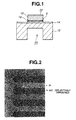
- a first protective film 14 made of platinum is formed over the entire surface of a substrate (e.g. an electroformed nickel substrate) 12.
- This first protective film 14 is formed with a preferred film thickness of 50 nm or more. Particularly, it is preferred that the film thickness be 100 nm or more.
- a preferred upper limit of the film thickness of the first protective film is 1 ⁇ m or less, under the circumstance of which platinum has a low membrane stress.
- the first protective film is formed by, for example, sputtering. As for specific conditions of sputtering, the film is formed with a film thickness of 200 nm by using a DC sputtering device at a substrate heating temperature of 150°C and with an output of 1000 W.
- a base film 16 made of titanium is then formed over the entire surface of the first protective film 14 made of platinum. Platinum can prevent the seed crystal for PZT described later from being formed over the substrate beyond a specified pattern. Titanium causes the seed crystal for PZT to be deposited and also causes a PZT film to grow and be formed by using such seed crystal as the nucleus. As the seed crystal for PZT, seed crystal with Sr or Ba substituted for a part of Pb from PZT can be used. The titanium film can be formed also by means of sputtering as in the case of the first protective film 14. The film thickness of the titanium film is about 0.5-1 ⁇ m.
- Etching is then performed on the titanium film with a mixed solution of aqueous hydrogen peroxide and ammonia in a specific pattern, that is, the pattern that will leave the titanium film above the ink cavity 20, on the basis of photolithography which utilizes a resist. Then, the PZT seed crystal is formed on the titanium film 16 over the substrate 12 by the following method.
- An aqueous lead nitrate solution (Pb(NO 3 ) 2 ), an aqueous zirconium oxychloride solution (ZrOCl 2 ), an aqueous titanium tetrachloride solution (TiCl 4 ) and an aqueous potassium hydroxide solution and, if necessary, an aqueous solution of strontium nitrate or barium chloride are mixed and adjusted to obtain a reaction solution.
- the above-described substrate is dipped in the reaction solution and a hydrothermal treatment is performed at a temperature of 140°C.
- a Ti source eluted from the titanium film 16 and a Ti source in the reaction solution are caused to react to a Pb source and a Zr source in the reaction solution, thereby forming the PZT seed crystal (seed crystal for the piezoelectric film) with a thickness of 0.1 ⁇ m over the surface of the titanium film. Since platinum which composes the first protective film 14 does not react to the reaction solution, the PZT seed crystal 6 is formed only over the titanium film 16.
- the back side of the substrate 12 with the PZT seed crystal 6 formed thereon is coated with fluororesin.
- This coated substrate 12 is then put in the above-described reaction solution at a temperature of 150°C and the hydrothermal treatment is performed for 12 hours. As a result, the PZT film has grown to become 10 ⁇ m thick.
- a lower electrode of this head is platinum which has electrical conductivity, that is, the first protective film 14.
- the first protective film 14 also functions as the lower electrode.
- the electroformed nickel substrate is used as the substrate 12.
- a silicon substrate, a processed form of other metal or ceramics, or a molded form of high polymer materials such as polysulfone can be used.
- Adhesively attaching a nozzle plate, which has a nozzle opening for discharging ink from the ink cavity 20, on the side of the ink cavity of the substrate 12 will complete an ink jet recording head.
- Figure 4 shows sectional views which illustrate the steps of manufacturing a piezoelectric film element according to Embodiment 2.
- the steps of manufacturing the piezoelectric film element are hereinafter explained in detail with reference to Figure 4 .
- Concerning Embodiment 2 the films (or members) similar to those in Embodiment 1 are given the same reference numeral and any detailed description thereof is omitted.
- a lower electrode forming film 3 is formed over a substrate (e.g. a silicon substrate) 1 through a silicon oxide film 2.
- a base film 16 made of titanium is then formed with a film thickness of about 0.5-1 ⁇ m over the lower electrode forming film 3.
- PZT seed crystal 6 is formed over the substrate 1 obtained in the step shown in Figure 4A in the same manner as that of Embodiment 1. At this time, because the Pb source in the reaction solution has active reactivity, the PZT seed crystal 6 is deposited partly over the surface of the second protective film 5.
- the second protective film 5 is removed from the substrate 1 obtained in the step shown in Figure 4B by means of wet etching with a potassium iodide solution.
- the PZT seed crystal 6 formed over the second protective film 5 in the step shown in Figure 4 B is removed together with the second protective film 5. This allows the PZT seed crystal 6 to be formed only in the area for forming the PZT film over the base film 16 formed on the substrate 1.
- a PZT film 18 is caused to grow by means of the hydrothermal synthesis over the PZT seed crystal 6 obtained in the step shown in Figure 4C .
- the reaction solution to be used for this hydrothermal reaction that used in Embodiment 1 can be utilized.
- the back side of the substrate 1 with the PZT seed crystal 6 formed thereon is coated with fluororesin.
- This coated substrate 1 is then put in the above-described reaction solution at a temperature of 150°C and the hydrothermal treatment is performed for 12 hours.
- the PZT film has grown to become 10 ⁇ m thick.
- the base film 16 with no PZT seed crystal formed thereon dissolves in the reaction solution.
- Embodiment 2 an explanation has been given about the case where silicon is used as the substrate. However, without limitation to such use, a processed form of metals or ceramics or a molded form of high polymer materials such as polysulfone may be used.
- a silicon oxide film 2 serving as a vibrating plate and a lower electrode 3 also serving as a vibrating plate are formed over a first surface of the substrate 1.
- the PZT film 18 and the upper electrode 22 are formed in a specified area (the area for forming the piezoelectric film element) on the lower electrode 3.
- the ink cavity 20 is formed at such a portion over the surface (a second surface) opposite to the first surface of the substrate 1 that corresponds to the area where the PZT film 18 is formed.
- a nozzle plate 10 with a nozzle opening 11 formed therein for discharging ink from the ink cavity 20 toward outside is provided.
- Embodiment 3 of this invention is hereinafter explained with reference to the relevant drawings.
- an amorphous nickel film 32 is formed with a film thickness of about 1-2 ⁇ m by means of electroforming over the surface of a substrate 12 made of electroformed nickel with an ink cavity 20 formed therein at a specified position.
- a base film 16 is then formed in the same manner as in Embodiment 1 over the substrate 12 with the amorphous nickel film 32 formed thereon on the surface opposite to the surface where the ink cavity 20 is formed.
- a second protective film 5 made of gold is selectively formed over the base film 16 at portions other than the area for forming the PZT film.
- PZT crystal seed 6 is then formed over the second protective film 5 and the base film 16 in the same manner as in Embodiment 1.
- a PZT film 18 is formed selectively only in the area for forming the PZT film in the same manner as in Embodiment 2.
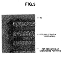
- FIGs 6 and 7 are photographs of the surface of the substrate 12 obtained in the above-described manner, which were taken by using an SEM (scanning electron microscope). It can be confirmed with these photographs that the PZT film 18 is formed selectively in desired areas.
- the PZT crystal growing step is performed in one step.
- the PZT crystal growing step is divided into several steps in order to control a PZT composition, a film thickness, a crystal grain diameter or other factors, it goes without saying that similar effects can be obtained even if the removal of the second protective film 5 is performed in the middle of the crystal growing step.
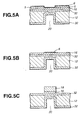
- Figure 8 is a photograph, which was taken by using an SEM, of the surface of the substrate (for comparison) with the PZT film formed thereon in the manner described above. It can be confirmed with this photograph that the PZT film is deposited also partly on the substrate (electroformed nickel).
- Embodiment 4 of this invention is hereinafter explained with reference to the relevant drawing.
- Figure 9 shows sectional views which illustrate the steps of manufacturing a piezoelectric film element according to Embodiment 4.
- the steps of manufacturing the piezoelectric film element are hereinafter explained in detail with reference to Figure 9 .
- Concerning Embodiment 4 detailed descriptions of the steps similar to those of the aforementioned embodiments are omitted and the films (or members) similar to those in the aforementioned embodiments are given the same reference numeral.
- a base film 16 is formed over a substrate 12 made of electroformed nickel in the same manner as in the aforementioned embodiments.
- a second protective film 25 made of platinum is then formed selectively at portions other than the area for forming a PZT film over the base film 16.
- PZT seed crystal 6 is formed in the same manner as in the aforementioned embodiments.
- the second protective film 25 is removed by means of ion milling by using the third protective film 21 as a mask.
- the third protective film 21 is removed. Consequently, the PZT seed crystal is selectively formed only in the area for forming the PZT film.
- the PZT seed crystal 6 is caused to grow and form a PZT film 18 in the same manner as in the aforementioned embodiments.
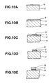
- Figure 10 shows sectional views which illustrate the steps of manufacturing a piezoelectric film element according to the example.
- the steps of manufacturing the piezoelectric film element are hereinafter explained in detail with reference to Figure 10 .
- Concerning the example detailed descriptions of the steps similar to those of the aforementioned embodiments are omitted and the films (or members) similar to those in the aforementioned embodiments are given the same reference numeral.
- a base film 16 is formed with a film thickness of about 0.5-1 ⁇ m over a substrate 41 made of nickel.
- PZT seed crystal 6 is formed by means of the hydrothermal synthesis over the base film 16 obtained in the step shown in Figure 10A .
- the base film 16 with the PZT seed crystal 6 formed thereon is selectively removed by using the mixed solution of aqueous hydrogen peroxide and ammonium.
- the PZT seed crystal may be selectively removed by means of ion milling.
- this invention can provide a piezoelectric film element with no deterioration of adhesion between the first protective film and the substrate, and a method of manufacturing such a piezoelectric film element. Moreover, it is possible to provide a piezoelectric film element with such a minute piezoelectric film pattern formed thereon as that of an ink jet recording head, and a method of manufacturing such a piezoelectric film element.
- this invention can form a minute piezoelectric film element of high precision at a specified position by means of the hydrothermal synthesis, it is possible to obtain a micro-actuator with good characteristics. Because the hydrothermal synthesis includes only low temperature process, the versatility of possible substrate materials to be used and sizes of the substrate is high, thereby it is possible to manufacture a long ink jet recording head like a line head.
- the piezoelectric film with excellent piezoelectric properties can be formed selectively in a specified area without lowering the dimensional precision of the substrate.
Landscapes
- Engineering & Computer Science (AREA)
- Manufacturing & Machinery (AREA)
- Chemical & Material Sciences (AREA)
- Ceramic Engineering (AREA)
- Particle Formation And Scattering Control In Inkjet Printers (AREA)
Claims (18)
- Piezoelektrisches Filmelement, das über einem Substrat umfasst:einen piezoelektrischen Film (18); undeine gemeinsame Elektrode und eine einzelne Elektrode (22), die so angeordnet sind, dass der piezoelektrische Film (18) zwischen ihnen aufgenommen ist,wobei es so gestaltet ist, dass Verformung des piezoelektrischen Films (18) bewirkt wird, indem über die gemeinsame Elektrode und die einzelne Elektrode Spannung an den piezoelektrischen Film (18) angelegt wird, wobei das piezoelektrische Filmelement (18) dadurch gekennzeichnet ist, dass es umfasst:einen ersten schützenden Film (14), der über der gesamten Fläche des Substrats (12) ausgebildet ist, um das Substrat (12) zu schützen und die Ausbildung des piezoelektrischen Films (18) auf dem Substrat (12) zu vermeiden; undeinen Basisfilm (16), der über dem ersten schützenden Film (14) in dem Bereich zum Ausbilden des piezoelektrischen Films (18) ausgebildet ist und als eine Basis dient, wenn veranlasst wird, dass der piezoelektrische Film (18) wächst, um ihn auszubilden, undwobei das piezoelektrische Filmelement des Weiteren dadurch gekennzeichnet ist, dass der piezoelektrische Film (18) über dem Basisfilm (16) ausgebildet ist.
- Piezoelektrisches Filmelement nach Anspruch 1, wobei der erste schützende Film (14) die gemeinsame Elektrode ist und die einzelne Elektrode (22) über dem piezoelektrischen Film (18) ausgebildet ist.
- Piezoelektrisches Filmelement nach Anspruch 1 oder 2, wobei der Basisfilm (16) der Film zum Ausbilden eines Keimkristalls für den piezoelektrischen Film (18) ist.
- Piezoelektrisches Filmelement nach Anspruch 3, wobei der piezoelektrische Film (18) aus einem hydrothermisch synthetisierten PZT-Film besteht und der Basisfilm (16) aus einem Titanfilm zum Ausbilden des Keimkristalls für den PZT-Film besteht.
- Piezoelektrisches Filmelement nach Anspruch 1, wobei der schützende Film (14) aus Gold, Platin oder Iridium hergestellt ist.
- Piezoelektrisches Filmelement nach Anspruch 3, wobei der erste schützende Film (14) eine Filmdicke von 50 nm hat, so dass kein Keimkristall (6) für den piezoelektrischen Film (18) an seiner Oberfläche ausgebildet wird.
- Piezoelektrisches Filmelement nach einem der Ansprüche 1, 3 oder 6,
wobei das Substrat (12) ein galvanogeformtes Substrat ist und amorphes Nickel als der erste schützende Film (32) über der Oberfläche des Substrats (12) ausgebildet ist. - Verfahren zum Herstellen eines piezoelektrischen Filmelementes, wobei das piezoelektrische Filmelement über einem Substrat (12) umfasst:einen piezoelektrischen Film (18); undeine gemeinsame Elektrode und eine einzelne Elektrode (22), die so angeordnet sind, dass der piezoelektrische Film (18) zwischen ihnen aufgenommen ist,wobei es so gestaltet ist, dass Verformung des piezoelektrischen Films (18) bewirkt wird, indem über die gemeinsame Elektrode und die einzelne Elektrode Spannung an den piezoelektrischen Film (18) angelegt wird,
wobei das Herstellungsverfahren die folgenden Schritte umfasst:Ausbilden eines ersten schützenden Films (14) über der gesamten Oberfläche des Substrats (12), um das Substrat (12) zu schützen und die Ausbildung des piezoelektrischen Films (18) auf dem Substrat zu vermeiden;Ausbilden eines Basisfilms (16), der als eine Basis dient, wenn veranlasst wird, dass der piezoelektrische Film (18) wächst, um ihn auszubilden, über dem ersten schützenden Film (14) in den Bereich zum Ausbilden des piezoelektrischen Films (18); undAusbilden eines Keimkristalls (6) für die Ausbildung des piezoelektrischen Films (18) über dem Substrat (12),Ausbilden des piezoelektrischen Films (18) über dem Basisfilm (16). - Verfahren zum Herstellen eines piezoelektrischen Filmelementes, wobei das piezoelektrische Filmelement über einem Substrat (12) umfasst:einen piezoelektrischen Film (18); undeine gemeinsame Elektrode und eine einzelne Elektrode, die so angeordnet sind, dass der piezoelektrische Film (18) zwischen ihnen aufgenommen wird,wobei es so gestaltet ist, dass Verformung des piezoelektrischen Films (18) bewirkt wird, indem über die gemeinsame Elektrode und die einzelne Elektrode Spannung an den piezoelektrischen Film (18) angelegt wird,
wobei das Herstellungsverfahren die folgenden Schritte umfasst:Ausbilden eines ersten schützenden Films über der gesamten Oberfläche des Substrats (12), um das Substrat (12) zu schützen und die Ausbildung des piezoelektrischen Films (18) auf dem Substrat (12) zu vermeiden;Ausbilden eines Basisfilms (16), der als eine Basis dient, wenn veranlasst wird, dass der piezoelektrische Film (18) wächst, um ihn auszubilden, über dem ersten schützenden Film;Ausbilden eines zweiten schützenden Films (5), der alkalibeständig ist, über dem Basisfilm (16) in einem anderen Bereich als dem Bereich zum Ausbilden des piezoelektrischen Films (18);Ausbilden eines Keimkristalls (6) für die Ausbildung des piezoelektrischen Films (18) über dem Substrat (12) mit dem darauf ausgebildeten zweiten schützenden Film (5); Entfernen des zweiten schützenden Films (5) von dem Substrat (12) mit dem darauf ausgebildeten Keimkristall (6); undVeranlassen von Kristallwachstum des Keimkristalls (6) nach Entfernen des zweiten schützenden Films (5). - Verfahren zum Herstellen eines piezoelektrischen Filmelementes nach Anspruch 9, das des Weiteren die folgenden Schritte umfasst:Ausbilden eines dritten schützenden Films (21) nach der Ausbildung des Keimkristalls (6), um den über dem Bereich zum Ausbilden des piezoelektrischen Films (18) ausgebildeten Keimkristall (6) zu schützen; undEntfernen des zweiten schützenden Films (5) nach der Ausbildung des dritten schützenden Films (21) und anschließend Entfernen des dritten schützenden Films (21).
- Verfahren zum Herstellen eines piezoelektrischen Filmelementes nach Anspruch 8, wobei der Basisfilm mit einem Film zum Ausbilden des Keimkristalls nach dem Ausbilden des piezoelektrischen Films ausgebildet wird.
- Verfahren zum Herstellen eines piezoelektrischen Filmelementes nach einem der Ansprüche 8 bis 11, wobei der piezoelektrische Film (18) unter Verwendung einer hydrothermischen Synthese ausgebildet wird und der Basisfilm (16) mit einem Titanfilm zum Ausbilden eines Keimkristalls für den durch die hydrothermische Synthese ausgebildeten PZT-Film ausgebildet wird.
- Verfahren zum Herstellen eines piezoelektrischen Filmelementes nach Anspruch 8, wobei der erste schützende Film (14) aus Gold, Platin oder Iridium hergestellt wird.
- Verfahren zum Herstellen eines piezoelektrischen Filmelementes nach Anspruch 8, wobei der erste schützende Film (14) mit einer Filmdicke von 50 nm oder mehr so ausgebildet wird, dass kein Keimkristall (6) für den piezoelektrischen Film auf seiner Oberfläche ausgebildet wird.
- Verfahren zum Herstellen eines piezoelektrischen Filmelementes nach Anspruch 9, wobei der zweite schützende Film (5) aus Gold hergestellt wird.
- Verfahren zum Herstellen eines piezoelektrischen Filmelementes nach Anspruch 8 oder 9, wobei das Substrat (12) aus galvanogeformtem Nickel besteht und ein Film (32) aus amorphem Nickel über der Oberfläche des galvanogeformten Nickels ausgebildet wird.
- Piezoelektrisches Filmelement, das mit einem Herstellungsverfahren nach einem der Ansprüche 8 bis 16 ausgebildet wird, wobei das Substrat (12) durch Galvanoformen hergestellt wird und amorphes Nickel, Kupfer oder Eisen über der Oberfläche des Substrats (12) ausgebildet wird.
- Tintenstrahl-Aufzeichnungskopf, der als eine Antriebsquelle zum Ausstoßen von Tinte ein piezoelektrisches Filmelement nach einem der Ansprüche 1 bis 7 und 17 verwendet.
Applications Claiming Priority (6)
| Application Number | Priority Date | Filing Date | Title |
|---|---|---|---|
| JP16428097 | 1997-06-20 | ||
| JP16428097A JP3615644B2 (ja) | 1997-06-20 | 1997-06-20 | 薄膜圧電体素子の製造方法及び薄膜圧電体素子、並びにインクジェット式記録ヘッド |
| JP164280/97 | 1997-06-20 | ||
| JP115093/98 | 1998-04-24 | ||
| JP11509398 | 1998-04-24 | ||
| JP11509398A JPH11307832A (ja) | 1998-04-24 | 1998-04-24 | 圧電体薄膜素子、その製造方法、並びにインクジェット式記録ヘッド |
Publications (3)
| Publication Number | Publication Date |
|---|---|
| EP0886328A2 EP0886328A2 (de) | 1998-12-23 |
| EP0886328A3 EP0886328A3 (de) | 2000-09-20 |
| EP0886328B1 true EP0886328B1 (de) | 2008-05-28 |
Family
ID=26453693
Family Applications (1)
| Application Number | Title | Priority Date | Filing Date |
|---|---|---|---|
| EP98111356A Expired - Lifetime EP0886328B1 (de) | 1997-06-20 | 1998-06-19 | Piezoelektrisches Schichtelement, Verfahren zum Herstellen und Tintenstrahldruckkopf |
Country Status (3)
| Country | Link |
|---|---|
| US (1) | US6147438A (de) |
| EP (1) | EP0886328B1 (de) |
| DE (1) | DE69839540D1 (de) |
Families Citing this family (17)
| Publication number | Priority date | Publication date | Assignee | Title |
|---|---|---|---|---|
| DE69934175T2 (de) * | 1998-08-12 | 2007-03-08 | Seiko Epson Corp. | Piezoelektrischer Aktuator, Tintenstrahlkopf, Drucker, Herstellungsverfahren für den piezoelektrischen Aktuator, Herstellungsverfahren für den Tintenstrahlkopf |
| US6594875B2 (en) * | 1998-10-14 | 2003-07-22 | Samsung Electro-Mechanics Co. | Method for producing a piezoelectric/electrostrictive actuator |
| JP3517876B2 (ja) | 1998-10-14 | 2004-04-12 | セイコーエプソン株式会社 | 強誘電体薄膜素子の製造方法、インクジェット式記録ヘッド及びインクジェットプリンタ |
| GB2345379B (en) * | 1998-12-30 | 2000-12-06 | Samsung Electro Mech | Method for fabricating piezoelectric/electrostrictive thick film using seeding layer |
| US6903491B2 (en) | 2001-04-26 | 2005-06-07 | Matsushita Electric Industrial Co., Ltd. | Piezoelectric element, actuator, and inkjet head |
| US6620237B2 (en) | 2001-11-15 | 2003-09-16 | Spectra, Inc. | Oriented piezoelectric film |
| US7009328B2 (en) * | 2003-06-20 | 2006-03-07 | Ngk Insulators, Ltd. | Piezoelectric/electrostrictive device made of piezoelectric/electrostrictive film and manufacturing method |
| CN1856403B (zh) * | 2003-09-24 | 2010-06-02 | 精工爱普生株式会社 | 液体喷头、其制造方法以及液体喷射设备 |
| JP4024741B2 (ja) * | 2003-10-20 | 2007-12-19 | 富士通メディアデバイス株式会社 | 圧電薄膜共振子及びフィルタ |
| BRPI0707339A2 (pt) * | 2006-01-30 | 2011-05-03 | Donaldson Co Inc | arranjo de filtro e métodos |
| US20090314727A1 (en) * | 2006-02-07 | 2009-12-24 | Donaldson Company, Inc. | Filter arrangement and methods |
| JP5275698B2 (ja) * | 2008-06-17 | 2013-08-28 | 富士フイルム株式会社 | 圧電体膜の分極方法および圧電素子構造体の製造方法 |
| WO2012118995A1 (en) * | 2011-03-02 | 2012-09-07 | Game Changers, Llc | Thermal transpiration device and method of making same |
| CN102834943B (zh) * | 2011-03-25 | 2015-09-09 | 日本碍子株式会社 | 层叠体及其制造方法 |
| CN105428518B (zh) * | 2015-11-13 | 2019-01-25 | 中国科学院上海微系统与信息技术研究所 | 基于局域共振体的声子晶体结构及其制作方法 |
| JP6690253B2 (ja) * | 2016-01-22 | 2020-04-28 | 株式会社リコー | Pzt前駆体溶液及びその製造方法、pzt膜の製造方法、電気機械変換素子の製造方法、液体吐出ヘッドの製造方法 |
| CN113272982B (zh) * | 2018-11-09 | 2024-06-14 | 麦斯卓微电子(南京)有限公司 | 压电致动器制造方法 |
Family Cites Families (7)
| Publication number | Priority date | Publication date | Assignee | Title |
|---|---|---|---|---|
| JP3244311B2 (ja) * | 1992-09-28 | 2002-01-07 | ローム株式会社 | 半導体装置の製造方法 |
| JP3159561B2 (ja) * | 1993-03-29 | 2001-04-23 | ローム株式会社 | 結晶性薄膜用電極 |
| JPH06349324A (ja) * | 1993-06-04 | 1994-12-22 | Sharp Corp | 強誘電体薄膜の形成方法 |
| JPH08118662A (ja) * | 1994-10-26 | 1996-05-14 | Mita Ind Co Ltd | インクジェットプリンタ用印字ヘッド及びその製造方法 |
| JP3166535B2 (ja) * | 1995-03-01 | 2001-05-14 | 富士電機株式会社 | インクジェット記録ヘッド |
| US5933167A (en) * | 1995-04-03 | 1999-08-03 | Seiko Epson Corporation | Printer head for ink jet recording |
| JP3209082B2 (ja) * | 1996-03-06 | 2001-09-17 | セイコーエプソン株式会社 | 圧電体薄膜素子及びその製造方法、並びにこれを用いたインクジェット式記録ヘッド |
-
1998
- 1998-06-19 EP EP98111356A patent/EP0886328B1/de not_active Expired - Lifetime
- 1998-06-19 DE DE69839540T patent/DE69839540D1/de not_active Expired - Lifetime
- 1998-06-22 US US09/100,882 patent/US6147438A/en not_active Expired - Lifetime
Also Published As
| Publication number | Publication date |
|---|---|
| DE69839540D1 (de) | 2008-07-10 |
| EP0886328A3 (de) | 2000-09-20 |
| EP0886328A2 (de) | 1998-12-23 |
| US6147438A (en) | 2000-11-14 |
Similar Documents
| Publication | Publication Date | Title |
|---|---|---|
| EP0886328B1 (de) | Piezoelektrisches Schichtelement, Verfahren zum Herstellen und Tintenstrahldruckkopf | |
| EP0794579B1 (de) | Piezoelektrische Dünnschichtanordnung | |
| EP1367658B1 (de) | "piezoelektrisches element, tintenstrahlkopf, winkelgeschwindigkeitssensor, herstellungsverfahren dafür und aufzeichnungsvorrichtung des tintenstrahltyps" | |
| US5802686A (en) | Process for the preparation of an ink jet printer head | |
| US7312558B2 (en) | Piezoelectric element, ink jet head, angular velocity sensor, and ink jet recording apparatus | |
| KR100978145B1 (ko) | 에피택셜 산화물막, 압전막, 압전막 소자, 압전막 소자를이용한 액체 토출 헤드 및 액체 토출 장치 | |
| US20030222947A1 (en) | Piezoelectric element, ink jet head, angular velocity sensor, method for manufacturing the same, and ink jet recording apparatus | |
| US6432546B1 (en) | Microelectronic piezoelectric structure and method of forming the same | |
| EP1033250B1 (de) | Piezoelektrisches Antriebselement, Tintenstrahldruckkopf, Herstellungsverfahren dafür, und Tintenstrahldrucker | |
| HK1008143B (en) | Printed head for ink jet recording and process for the preparation thereof | |
| JP3666163B2 (ja) | 圧電体素子及びこれを用いたアクチュエータ並びにインクジェット式記録ヘッド | |
| JP2003081694A (ja) | 強誘電体薄膜及びその製造方法 | |
| EP0932210B1 (de) | Piezoelektrisches Schichtelement und Tintenstrahldruckkopf, der dieses benutzt | |
| JP3734176B2 (ja) | インクジェット記録用プリンタヘッドの製造方法及びアクチュエータの製造方法 | |
| JP3615644B2 (ja) | 薄膜圧電体素子の製造方法及び薄膜圧電体素子、並びにインクジェット式記録ヘッド | |
| JPH11307832A (ja) | 圧電体薄膜素子、その製造方法、並びにインクジェット式記録ヘッド | |
| JP3682839B2 (ja) | 圧電体素子、インクジェット式記録ヘッド、プリンタおよび圧電体素子の製造方法 | |
| WO2003010834A2 (en) | Microelectronic piezoelectric structure | |
| JP2023134333A (ja) | 結晶、積層構造体、電子デバイス、電子機器及びこれらの製造方法 | |
| JP3478095B2 (ja) | 強誘電体薄膜素子およびその製造方法 | |
| JP2006510566A (ja) | 蒸着法を用いた強誘電性単結晶膜構造物の製造方法 | |
| JP4066518B2 (ja) | 圧電結晶薄膜とその製造方法、および圧電体素子 | |
| JP2005236269A (ja) | 圧電素子及びその製造方法並びに液体噴射ヘッド | |
| EP4471191A1 (de) | Mehrschichtige struktur, elektronische vorrichtung, elektronische vorrichtung und herstellungsverfahren dafür | |
| EP4686371A1 (de) | Piezoelektrischer mehrschichtkörper, piezoelektrischer mehrschichtwafer und verfahren zur herstellung eines piezoelektrischen mehrschichtkörpers |
Legal Events
| Date | Code | Title | Description |
|---|---|---|---|
| PUAI | Public reference made under article 153(3) epc to a published international application that has entered the european phase |
Free format text: ORIGINAL CODE: 0009012 |
|
| AK | Designated contracting states |
Kind code of ref document: A2 Designated state(s): DE FR GB IT NL |
|
| AX | Request for extension of the european patent |
Free format text: AL;LT;LV;MK;RO;SI |
|
| PUAL | Search report despatched |
Free format text: ORIGINAL CODE: 0009013 |
|
| AK | Designated contracting states |
Kind code of ref document: A3 Designated state(s): AT BE CH CY DE DK ES FI FR GB GR IE IT LI LU MC NL PT SE |
|
| AX | Request for extension of the european patent |
Free format text: AL;LT;LV;MK;RO;SI |
|
| RIC1 | Information provided on ipc code assigned before grant |
Free format text: 7H 01L 41/09 A, 7H 01L 41/24 B |
|
| 17P | Request for examination filed |
Effective date: 20001114 |
|
| AKX | Designation fees paid |
Free format text: DE FR GB IT NL |
|
| RAP1 | Party data changed (applicant data changed or rights of an application transferred) |
Owner name: SEIKO EPSON CORPORATION |
|
| 17Q | First examination report despatched |
Effective date: 20040121 |
|
| 17Q | First examination report despatched |
Effective date: 20040121 |
|
| GRAP | Despatch of communication of intention to grant a patent |
Free format text: ORIGINAL CODE: EPIDOSNIGR1 |
|
| GRAS | Grant fee paid |
Free format text: ORIGINAL CODE: EPIDOSNIGR3 |
|
| GRAA | (expected) grant |
Free format text: ORIGINAL CODE: 0009210 |
|
| AK | Designated contracting states |
Kind code of ref document: B1 Designated state(s): DE FR GB IT NL |
|
| REG | Reference to a national code |
Ref country code: GB Ref legal event code: FG4D |
|
| REF | Corresponds to: |
Ref document number: 69839540 Country of ref document: DE Date of ref document: 20080710 Kind code of ref document: P |
|
| PG25 | Lapsed in a contracting state [announced via postgrant information from national office to epo] |
Ref country code: NL Free format text: LAPSE BECAUSE OF FAILURE TO SUBMIT A TRANSLATION OF THE DESCRIPTION OR TO PAY THE FEE WITHIN THE PRESCRIBED TIME-LIMIT Effective date: 20080528 |
|
| NLV1 | Nl: lapsed or annulled due to failure to fulfill the requirements of art. 29p and 29m of the patents act | ||
| PLBE | No opposition filed within time limit |
Free format text: ORIGINAL CODE: 0009261 |
|
| STAA | Information on the status of an ep patent application or granted ep patent |
Free format text: STATUS: NO OPPOSITION FILED WITHIN TIME LIMIT |
|
| GBPC | Gb: european patent ceased through non-payment of renewal fee |
Effective date: 20080828 |
|
| 26N | No opposition filed |
Effective date: 20090303 |
|
| PG25 | Lapsed in a contracting state [announced via postgrant information from national office to epo] |
Ref country code: IT Free format text: LAPSE BECAUSE OF FAILURE TO SUBMIT A TRANSLATION OF THE DESCRIPTION OR TO PAY THE FEE WITHIN THE PRESCRIBED TIME-LIMIT Effective date: 20080528 |
|
| PG25 | Lapsed in a contracting state [announced via postgrant information from national office to epo] |
Ref country code: GB Free format text: LAPSE BECAUSE OF NON-PAYMENT OF DUE FEES Effective date: 20080828 |
|
| REG | Reference to a national code |
Ref country code: FR Ref legal event code: ST Effective date: 20110617 |
|
| PG25 | Lapsed in a contracting state [announced via postgrant information from national office to epo] |
Ref country code: FR Free format text: LAPSE BECAUSE OF NON-PAYMENT OF DUE FEES Effective date: 20080728 |
|
| PGFP | Annual fee paid to national office [announced via postgrant information from national office to epo] |
Ref country code: DE Payment date: 20160614 Year of fee payment: 19 |
|
| REG | Reference to a national code |
Ref country code: DE Ref legal event code: R119 Ref document number: 69839540 Country of ref document: DE |
|
| PG25 | Lapsed in a contracting state [announced via postgrant information from national office to epo] |
Ref country code: DE Free format text: LAPSE BECAUSE OF NON-PAYMENT OF DUE FEES Effective date: 20180103 |