EP0889435A2 - Puce avec une rangée d'éléments à électroluminescence, circuit intégré de commande pour une rangée d'éléments à électroluminescence et tête d'impression - Google Patents
Puce avec une rangée d'éléments à électroluminescence, circuit intégré de commande pour une rangée d'éléments à électroluminescence et tête d'impression Download PDFInfo
- Publication number
- EP0889435A2 EP0889435A2 EP98305088A EP98305088A EP0889435A2 EP 0889435 A2 EP0889435 A2 EP 0889435A2 EP 98305088 A EP98305088 A EP 98305088A EP 98305088 A EP98305088 A EP 98305088A EP 0889435 A2 EP0889435 A2 EP 0889435A2
- Authority
- EP
- European Patent Office
- Prior art keywords
- light emitting
- drive
- pad electrodes
- scan
- data
- Prior art date
- Legal status (The legal status is an assumption and is not a legal conclusion. Google has not performed a legal analysis and makes no representation as to the accuracy of the status listed.)
- Granted
Links
Images





Classifications
-
- G—PHYSICS
- G06—COMPUTING OR CALCULATING; COUNTING
- G06K—GRAPHICAL DATA READING; PRESENTATION OF DATA; RECORD CARRIERS; HANDLING RECORD CARRIERS
- G06K15/00—Arrangements for producing a permanent visual presentation of the output data, e.g. computer output printers
- G06K15/02—Arrangements for producing a permanent visual presentation of the output data, e.g. computer output printers using printers
- G06K15/12—Arrangements for producing a permanent visual presentation of the output data, e.g. computer output printers using printers by photographic printing, e.g. by laser printers
- G06K15/1238—Arrangements for producing a permanent visual presentation of the output data, e.g. computer output printers using printers by photographic printing, e.g. by laser printers simultaneously exposing more than one point
- G06K15/1242—Arrangements for producing a permanent visual presentation of the output data, e.g. computer output printers using printers by photographic printing, e.g. by laser printers simultaneously exposing more than one point on one main scanning line
- G06K15/1247—Arrangements for producing a permanent visual presentation of the output data, e.g. computer output printers using printers by photographic printing, e.g. by laser printers simultaneously exposing more than one point on one main scanning line using an array of light sources, e.g. a linear array
-
- B—PERFORMING OPERATIONS; TRANSPORTING
- B41—PRINTING; LINING MACHINES; TYPEWRITERS; STAMPS
- B41J—TYPEWRITERS; SELECTIVE PRINTING MECHANISMS, i.e. MECHANISMS PRINTING OTHERWISE THAN FROM A FORME; CORRECTION OF TYPOGRAPHICAL ERRORS
- B41J2/00—Typewriters or selective printing mechanisms characterised by the printing or marking process for which they are designed
- B41J2/435—Typewriters or selective printing mechanisms characterised by the printing or marking process for which they are designed characterised by selective application of radiation to a printing material or impression-transfer material
- B41J2/447—Typewriters or selective printing mechanisms characterised by the printing or marking process for which they are designed characterised by selective application of radiation to a printing material or impression-transfer material using arrays of radiation sources
- B41J2/45—Typewriters or selective printing mechanisms characterised by the printing or marking process for which they are designed characterised by selective application of radiation to a printing material or impression-transfer material using arrays of radiation sources using light-emitting diode [LED] or laser arrays
Definitions
- the present invention relates to a print head that is employed as a exposure light source for forming an electrostatic latent image on a photosensitive body in a printing apparatuses such as printers and facsimile machines adopting the electrophotographic printing system, and the present invention also relates to a matrix-type light emitting element array chip to constitute the print head and a light emitting element array drive IC that drives the matrix-type light emitting element array chip.
- Print heads that are employed as an exposure light source for a photosensitive body in a printing apparatus adopting the electrophotographic printing system in the prior art include those that use as a light source, a light emitting element array constituted by providing a number of light emitting elements such as semiconductor laser elements, LED elements and the like in a single row, and those that use a fluorescent light, a cold-cathode tube or the like as a light source and use a liquid crystal element as a shutter.
- Those different types of print heads all selectively expose the photosensitive body that has been uniformly charged by a charger with the light source to form an electrostatic latent image on the photosensitive body.
- an LED array a light emitting element array achieved by providing a great number of LED elements
- a print head constituted with an LED array is referred to as an LED print head.
- An LED print head may be constituted by mounting on a mounting substrate LED array chips each achieved by providing a great number of LED elements on a single semiconductor chip and light emitting element array drive ICs each provided for controlling light emission of the individual LED elements in each of the LED array chips, in quantities that correspond to the printing width.
- FIG. 8 is a top view illustrating the structure of an LED array chip in the prior art.
- the LED array chip 51 illustrated in FIG. 8 is provided with LED elements 52 provided in a single row, individual pad electrodes to be driven 53 that are individually connected to the anodes of the LED elements 52 and a common electrode 54 that is connected to the cathodes of all the LED elements 52.
- the common electrode 54 is provided at the rear surface of the LED array chip 51.
- FIG. 9 is a partial enlargement of an LED print head in the prior art mounted with the LED array chip illustrated in FIG. 8.
- the LED print pad illustrated in FIG. 9 is constituted by mounting the LED array chip 51 and an LED array drive IC 55 for driving the LED array chip 51 at a mounting substrate 59.
- the individual pad electrodes to be driven 53 of the LED array chip 51 and drive pad electrodes 60 of the LED array drive IC 55 are connected with each other through metal wires 56, and I/O pad electrodes 61 of the LED array drive IC 55 are connected with wiring patterns (conductive patterns) 62 for control signals and the source formed at the mounting substrate 59.
- the common electrode 54 formed at the rear surface of the LED array chip 51 is connected to a cathode wiring pattern (conductive pattern) 58 formed at the mounting substrate 59.
- the LED array drive IC 55 is provided with a shift register that stores individual sets of data that have been input, drive current source circuits each of which outputs a drive current corresponding to one of the individual sets of data and switching circuits that turn ON/OFF between the output terminals of the drive source circuit and the drive pad electrodes 60 in conformance with the strobe signal that has been input.
- the number of shift register stages, the number of drive current source circuits, the number of switching circuits and the number of drive pad electrodes 60 all correspond to the number of LED elements 52 at the LED array chip 51.
- a drive current is output by, for instance, the drive current source circuit corresponding to the printing data that indicate light emission, and with the switching circuits set to ON while the strobe signal is at "H” level, the drive current is supplied to the LED elements 52 that correspond to the printing data at "L” level via the individual pad electrodes 53 to be driven to achieve selective light emission.
- the anodes of the LED elements 52 at the LED array chip 51 are connected to the individual pad electrodes 53 to be driven (the drive pad electrodes 60 at the drive IC 55) on a one-to-one basis.
- a matrix-type LED array chip such as that disclosed in Japanese Unexamined Patent Publication No. 1987-152873 provides a solution to this problem.
- matrix-connections are achieved between M ⁇ N light emitting elements and M pad electrodes to be scanned connected to the cathodes of the light emitting elements and between the light emitting elements and N pad electrodes to be driven connected to the anodes of the light emitting elements, in order to reduce the number of pad electrodes in the LED array chip.
- a matrix-type LED array chip may assume a structure, for instance, in which, a semiconductor chip is divided into M semiconductor blocks, a pad electrode to be scanned and N light emitting elements are formed on each semiconductor block and N pad electrodes to be driven are formed on the M semiconductor blocks, with the cathodes of the N LED elements within each block connected with the pad electrode to be scanned within the block and the anodes of the N LED elements within the block individually connected with different pad electrodes to be driven.
- drive ICs drive circuits
- data control IC data control circuit
- scan control IC scan control circuit
- An object of the present invention which has been completed to address the problems in the prior art discussed above, is to provide a new and improved light emitting element array chip and a new and improved light emitting element array drive IC that achieve a reduction in the print head size and a reduction in production costs.
- Another object of the present invention is to provide a new and improved light emitting element array chip and a new and improved light emitting element array drive IC, that make it possible to directly bond the light emitting element array chip to the light emitting element array drive IC from one side of the chip so that the number of wiring patterns (conductive patterns) at the mounting substrate can be reduced.
- Yet another object of the present invention is to provide a new and improved light emitting element array chip and a new and improved light emitting element array drive IC, that preclude the necessity for mounting two types of drives ICs, i.e., an operation control IC and a data control IC, when mounting the light emitting element array chip, to achieve a reduction in the number of drive ICs.
- drives ICs i.e., an operation control IC and a data control IC
- Still another object of the present invention is to provide a new and improved light emitting element array chip and a new and improved light emitting element array drive IC that achieve an improvement in the reliability of the product through direct bonding of the light emitting element array chip to the light emitting element array drive IC.
- a still further object of the present invention is to provide a new and improved light emitting element array chip and a new and improved light emitting element array drive IC that make it possible to improve the per line printing speed when they are employed in a printer head of printing apparatuses such as printers, facsimile machines and the like adopting the electrophotographic printing system.
- the light emitting element array chip according to the present invention which is provided with a plurality of pad electrodes to be scanned to which first electrodes of light emitting elements are connected, a plurality of pad electrodes to be driven to which second electrodes of the light emitting elements are connected and a plurality of the light emitting elements provided in a single row and is constituted by matrix-connecting the first electrodes and the second electrodes of the plurality of light emitting elements to the pad electrodes to be scanned and the pad electrodes to be driven, is characterized in that the plurality of pad electrodes to be scanned and the plurality of pad electrodes to be driven are positioned along one side on the lengthwise side of the chip.
- the light emitting element array drive IC which is a light emitting element array drive IC that drives a light emitting element array achieved by matrix-connecting Y ⁇ N light emitting elements to M pad electrodes to be scanned and N pad electrodes to be driven, is characterized in that it is provided with a scan control unit which performs scanning of the M pad electrodes to be scanned by sequentially validating the M pad electrodes to be scanned one at a time with the timing corresponding to a scan signal input from the outside and a data control unit that, each time the valid pad electrode to be scanned is switched, selectively drives the N pad electrodes to be driven based upon the individual sets of data corresponding to the light emitting elements input from the outside to selectively cause the N light emitting elements connected with the pad electrodes to be scanned that have become valid to emit light.
- the print head according to the present invention which is provided with a light emitting element array chip constituted by matrix-connecting Y ⁇ N light emitting elements to M pad electrodes to be scanned and N pad electrodes to be driven, a light emitting element array drive circuit that drives the light emitting element array chip and a mounting substrate on which the light emitting element array chip and the light emitting element array drive circuit are mounted, is characterized in that the light emitting element array chip according to the present invention is employed to constitute the light emitting element array chip or that the light emitting element array drive IC according to the present invention is employed to constitute the light emitting element array drive IC.
- FIG. 1 is a top view illustrating the structure of an LED print head in the embodiment of the present invention.
- the LED print head in FIG. 1 is constituted by mounting a plurality of matrix-type LED array chips 1 and a plurality of LED array drive ICs 10 at a mounting substrate 41.
- FIG. 2 is a top view illustrating the structure of each LED array chip 1
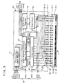
- FIG. 3 is a block diagram of each LED array drive IC 10.
- Pad electrodes to be driven 3 at an LED array chip 1 are connected with drive pad electrodes 16 of LED array drive IC 10 through metal wires 42a, whereas pad electrodes to be scanned 4 at the LED array chip 1 are connected with scan pad electrodes 17 of the LED array drive IC 10 through metal wires 42b.
- the wiring pattern (conductive pattern) for signals, sources and the like (not shown) provided on the mounting substrate 41 is connected with an I/O pad electrode 18 of the LED array drive IC 10 through metal wire 43.
- FIG. 2 schematically illustrates the wiring pattern (conductive pattern) of the LED array chip 1 according to the present invention.
- the first conduction-side referred to as the cathode side in reference to this embodiment
- the 16 LEDs within the first block constitute a common cathode side and this common cathode 7-1 is connected at a scan pad electrode 4-1.
- common cathodes 7-2, 7-3, ..., 7-16 are respectively connected at scan pad electrodes 4-2, 4-3, ..., 4-16.
- Separating areas 5-1 through 5-15 are provided to electrically isolate the common cathodes 7-1 through 7-16 from one another.
- Anode-side common wirings (conductive patterns) 9 connect LEDs of the same order among the individual blocks through anode-side individual electrode wirings (conductive patterns) 8 provided in correspondence to the individual LEDs at the second conduction-side (referred to as anode-side in reference to this embodiment).
- the anode-side individual wirings (conductive patterns) 8-1, 8-17, ..., 8-241 of LED (1,1) LED (2,1),..., LED (16,1) are connected at the anode-side common wiring (conductive pattern) 9-1
- the anode-side individual wirings (conductive patterns) 8-2, 8-18,..,8-243 of LED (1,2) LED(2,2),...LED (16,2) are connected at the anode-side common wiring (conductive pattern) 9-2 and so forth so that LEDs of the same order among the individual blocks are connected at 16 anode-side common wirings (conductive patterns).
- the anode-side common wirings (conductive patterns) 9-1 through 9-16 are respectively connected at drive pad electrodes 3-1 through 3-16.
- the LED array chip according to the present invention structured as described above is defined as a matrix LED array.
- the wiring (conductive pattern) achieved as described above is defined as a matrix conductive pattern.
- the connections of the common wiring (conductive pattern) 7 at the first electrode side with the scan pad electrodes 4 and of the individual wirings (conductive patterns) 8 at the second conduction-side connected at the second conduction-side common wirings (conductive patterns) 9 which are connected to the individual drive pad electrodes 3 in matrix wiring (conductive pattern) are generically termed as matrix connections of the first conduction-side electrodes (hereafter referred to as the first electrodes) to the scan pad electrodes and of the second conduction-side individual electrodes (hereafter referred to as the second electrodes) to the drive pad electrodes.
- the wiring (conductive pattern) formation area for the second electrodes 8-1, 8-2, ..., 8-16 and the second conduction-side common wirings (conductive patterns) 9-1, 9-2, ... 9-16 is defined as a matrix conductive
- the LED array according to the present invention is referred to as an M ⁇ N matrix LED array chip.
- M ⁇ N LEDs present within the M ⁇ N matrix LED array chip and LEDs 2-(i,1) through 2-(i,N) (1 ⁇ i ⁇ M) are commonly connected at their first conduction-side, constituting a first electrode 7-i which is connected to a scan pad electrode 4-i, with second electrodes 8-(i,j) (1 ⁇ i ⁇ M) of the individual LEDs 2-(1, j) through 2-(M,j) (1 ⁇ j ⁇ N) connected at a second conduction-side common wiring (conductive pattern) 9-j,which is connected at a drive pad electrode 3-j.
- N LED elements 2-(i, 1) through 2-(i, N) and a pad electrode to be scanned 4-i are formed.
- the pad electrode to be scanned 4-i is connected to the cathodes (first electrodes) of the LED elements 2-(i, 1) through 2-(i, N) formed at the block 7-i.
- N pad electrodes to be driven 3-1 through 3-N are formed at the LED array chip 1.
- a pad electrode to be driven 3-j (j represents one of the integers among 1 through N) is connected to the anodes (second electrodes) of the M LED elements 2-(1, j), 2-(2, j)... 2-(M, j) through the matrix wiring (conductive pattern) portion 6.
- a pad electrode 3-i is formed at the block 7-i.
- the LED array chip 1 is characterized in that the pad electrodes to be driven 3-1 through 3-N and the pad electrodes to be scanned 4-1 through 4-M are positioned in a single row along one side in the lengthwise direction of the LED array chip 1.
- the pad electrodes to be driven 3 and the pad electrodes to be scanned 4 are positioned alternately.
- the pad electrodes to be driven 3-1 through 3-N and the pad electrodes to be scanned 4-1 through 4-M may be each provided in single file.
- the pad electrodes to be driven 3-1 through 3-N and the pad electrodes to be scanned 4-1 through 4-M may be positioned over two rows (each row will comprise the pad electrodes to be driven 3 and the pad electrodes to be scanned 4).
- the blocks 7 are constituted by, for instance, growing an n-type semiconductor layer on a semi-insulating semiconductor substrate and dividing the n-type semiconductor layer into M n-type semiconductor blocks with separating grooves (isolation grooves) 5.
- the LED elements 2 may each be constituted by, for instance, forming a p-type semiconductor area which will constitute an anode at the n-type semiconductor block which will constitute a cathode.
- the blocks 7 may be constituted as p-type semiconductor blocks, with the anodes of the LED elements connected to the pad electrodes to be scanned and their cathodes connected to the pad electrodes to be driven, instead. In that case, the anodes of the LED elements constitute first electrodes and their cathodes constitute second electrodes.
- the operation of the LED array chip 1 is now explained.
- the 256 LED elements 2-(1, 1) through 2-(16, 16) of the LED array chip 1 each separately engage in a light emitting operation.
- the LED elements 2-(i, 1) through 2-(i, 16) connected to the pad electrodes to be driven 3-1 through 3-16 respectively, and the pad electrode to be scanned 4-i connected to the GND the LED elements 2-(i, 1) through 2-(i, 16) of the block 7-i are selectively caused to engage in a light emitting operation in correspondence to the individual sets of data.
- the 256 LED elements 2 are caused to individually engage in a light emitting operation.
- the LED array drive IC 10 is provided with a printing data shift register 11 (drive data shift register), a light quantity correction data shift register 12, a drive circuit 13 (means for drive), a scan data shift register 14, a scan circuit 15 (means for scanning), drive pad electrodes 16-1 through 16-N and scan pad electrodes 17-1 through 17-M.
- the printing data shift register data 11, the light quantity correction data shift register 12 and the drive circuit 13 constitute a data control unit.
- the scan data shift register 14 and the scan circuit 15 constitute a scan control unit.
- the LED array drive IC 10 is also provided with an I/O pad electrode 18 that is connected with the wiring (conductive pattern) pattern at the mounting substrate 41 illustrated in FIG. 1.
- the I/O pad electrode 18 is provided with four data input terminals DI1 through DI4 through which individual sets of data corresponding to the LED elements (printing data and light quantity correction data) are input, a shift clock input terminal SFC to which a shift clock is input, a scan clock input terminal SCC through which a scan clock is input, a strobe input terminal STB through which a strobe signal is input, a scan data input terminal SCD through which scan data are input and four data output terminals D01 through D04.
- the scan data and the scan clock constitute a scan signal.
- the data control unit and the scan control unit are both internally provided at the LED array drive IC 10 so that it can drive the matrix-type LED array chip 1 by itself.
- FIG. 4 illustrates the structure of the data control unit of the LED array drive IC 10.
- the printing data shift register 11 is provided with R ⁇ S (R represents an integer which is equal to the number of the data input terminals DI at the LED array drive IC 10, S represents a positive integer and R x S represents an integer equal to or larger than N) D flipflops.
- R ⁇ S flipflops 21 are indicated as 21-1 through 21-(R ⁇ S) or 21-(1, 1) 21-(2, 1)... 21-(R, 1), 21-(1, 2)... 21-(R, S).
- the D flipflops 21-(k, 4) through 21-(k, 1), (k represents one integer among 1 through R) are connected in series, and the data input terminal of the D flipflop 21-(k. 4) at the first stage is connected to the data input terminal D 1k.
- the clock input terminals of the 16 D flipflops 21-1 through 21-16 are commonly connected to the shift clock input terminal SFC.
- the light quantity correction shift register 12 is provided with R ⁇ N D flipflops 22-(1, 1) through 22-(R, N).
- the D flipflops 22-(k, 16) through 22-(k, 1) are connected in series, and the data input terminals of the D flipflops 22-(k, 16) at the first stage is connected to the data output terminal of the D flipflop 21-(k, 1) of the printing data shift register 11, whereas the data output terminal of the D flipflop 22-(k, 1) at the last stage is connected with the data output terminal DOk.
- the clock input terminals of the D flipflops 22-(1, 1) through 22-(4, 16) are commonly connected with the shift clock input terminal SFC.
- the printing data shift register 11 and the light quantity correction shift register 12 are connected in series.
- the drive circuit 13 is provided with drive current source circuits 23-1 through 23-N (drive source circuits), AND gates 24-1 through 24-N and switching transistors 25-1 through 25-N.
- the drive current source circuit 23-i is provided with four light quantity correction data input terminals and a drive current output terminal, with the four light quantity correction data input terminals respectively connected with the data output terminals of the D flipflops 22-(1, i) through 22-(4, i).
- the drive current source circuit 23-i sets a drive current value that corresponds to the light quantity correction data that have been input and outputs the drive current at this value through its drive current output terminal.
- First input terminals of the AND gates 24-1 through 24-N are commonly connected to the strobe input terminal STB.
- the second input terminal of the AND gate 24-i is connected to the data output terminal of the D flipflop 21-i.
- the base terminal of the switching transistor 25-i is connected to the output terminal of the AND gate 24-i, with the collector connected to the output terminal of the drive current source circuit 23-i and the emitter terminal connected to a constant current output electrode 16-i.
- the AND gate 24-i and the switching transistor 25-i constitute a switching circuit of the data control unit.
- FIG. 5 illustrates the structure of the scan control unit of the LED array drive IC 10.
- the scan data shift register 14 is provided with N D flip-flops 31-1 through 31-N that are connected in series and N scan output terminals SQ-lthrough SQ-N.
- the data input terminal D of the D flipflop 31-1 at the first stage is connected to the scan data input terminal SCD.
- the output terminal of the D flip-flop 31-i is connected to the scan output terminal SQ-i.
- the clock input terminals of the N D flipflops 31 are commonly connected to the scan clock input terminal SCC.
- the scan circuit 15 is provided with N AND gates 32-1 through 32-N and N switching transistors 33-1 through 33-N.
- First input terminals of the N AND gates 32 are commonly connected with the strobe input terminal STB.
- the second input terminal of the AND gate 32-i is connected to the scan output terminal SQ-i of the scan data shift register 14.
- the emitter electrodes of the N switching transistors 33 are grounded (are commonly connected to the GND).
- the base terminal of the switching transistor 33-i is connected to the output terminal of the AND gate 32-i whereas its collector terminal is connected to the scan pad electrode 17-i.
- the AND gate 32-i and the switching transistor 33-i constitute a switching circuits in the scan control unit.
- Different sets of printing data and light quantity correction data i. e., sets of printing data and light quantity correction data matching the corresponding LED array chips 1, are input through the data input terminals DI1 through DI4 of the plurality of LED array drive ICs 10 mounted at the mounting substrate 41.
- the printing data and the light quantity correction data are input from the outside of the mounting substrate 41 via the wiring (conductive pattern) pattern (not shown) at the mounting substrate and metal wires 43.
- a single shift clock is input through the shift clock input terminals SFC of all the LED array drive ICs 10.
- a common scan clock, a common set of scan data and a common strobe signal are input through the scan clock input terminals SCC, the scan data input terminals SCD and the strobe input terminals STB respectively of all the LED array drive ICs 10.
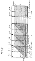
- FIG. 6 is a time chart of the operation of the LED array drive IC 10.
- (a) indicates the shift clock input through the shift clock input terminal SFC
- (b) through (e) indicate printing data and light quantity correction data input through the data input terminals DI1 through DI4
- (f) indicates the scan clock input through the scan clock input terminal SCC
- (g) indicates the scan data input through the scan data input terminal SCD.
- (h) through (j) indicate the waveforms at the scan output terminals SQ-1, SQ-2 and SQ-16 of the scan data shift register 14, and (k) indicates the strobe signal input through the strobe input terminal STB.
- the shift clock indicated by (a) constitutes an operating clock for the printing data shift register 11 and the light quantity correction data shift register 12, whereas the scan clock indicated by (f) constitutes an operating clock for the scan data shift register 14.
- the scan data indicated by (g) are used to sequentially cause the blocks 7-1 through 7-16 (their LED elements 2) of the LED array 1 to emit light and the strobe signal indicated by (k) is a signal for controlling the length of light emission time for the LED elements 2.
- the setting of the light quantity correction data may be implemented by following the procedure explained below, for instance.
- the LED elements 2 of the LED array chip 1 are caused to emit light one at a time, and by setting the drive current at varying values, the drive current value at which the quantity of the emitted light achieves a reference light quantity is measured. This measurement is performed for all 256 of the LED elements 2.
- the light quantity correction data are 4-bit data and written in a memory device such as a ROM.
- the drive current source circuits 23 of the LED array drive IC 10 each output a constant current determined by subtracting the correction current value based upon the light quantity correction data from the reference current value which may, for instance, 3mA.
- the drive current at the value at which the reference light quantity is achieved are output from the drive current source circuits 23 so that all the LED elements 2 emit light at the reference light quantity.
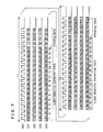
- FIG. 7 illustrates the data transfer format for the LED array drive IC 10.
- the light quantity correction data are input ahead of the printing data.
- the bit data b0-1 through b0-16 in the light quantity correction data and the printing data Q-1, Q-5, Q-9 and Q-13 are input through the data input terminal DI1.
- the bit data b1-1 through bl-16 in the light quantity correction data and the printing data Q-2, Q-6, Q-10 and Q-14 are input through the data input terminal DI2.
- bit data b2-1 through b2-16 in the light quantity correction data and the printing data Q-3, Q-7, Q-11 and Q-15 are input through the data input terminal DI3 and the bit data b3-1 through b3-16 in the light quantity correction data and the printing data Q-4, Q-8, Q-12 and Q-16 are input through the data input terminal DI4.
- the light quantity correction data for the LED element 2-i are stored at the D flipflops 22-(1, i) through 22-(4, i) of the light quantity correction register 12.
- the printing data corresponding to the LED element 2-i are stored at the D flipflop 21-i of the printing data shift register 11.
- the 4-bit light quantity correction data b0-1, b1-i, b2-i and b3-i stored at the light quantity correction shift register 12 are input through the drive current source circuit 23-i of the drive circuit 13, and the drive current source circuit 23-i, in turn, sets the drive current value in correspondence to the input light quantity correction data.
- the second input terminal of the AND gate 24-1 of the drive circuit 13 is set to either "H” or "L” level in conformance to the printing data Q-i stored at the printing data shift register 11.
- the first input terminals of the AND gates 24-1 through 24-16 are set to "L” and the switching transistors 25-1 through 25-16 are in an OFF state.
- the scan data at "H” level indicated by (g) in FIG. 6 are input through the terminal SCD, and these scan data are stored at the D flipflop 31-1 of the scan data shift register 14 using the scan clock input through the terminal SCC.
- the second input terminal of the AND gate 32-1 shifts from “L” level to "H” level while the second input terminals of the AND gates 32-2 through 32-16 remain at “L” level.
- the first input terminals of the AND gates 32-1 through 32-16 are at “L” level, with the switching transistors 33-1 through 33-16 set in an OFF state.
- the switching transistor 25-i becomes turned on, and a drive current flows from the drive current source circuit 23-i through a path extending from the drive pad electrode 16-i through the pad electrode to be driven 3-i, the LED element 2-i and the pad electrode to be scanned 4-1 to the scan pad electrode 17-1 to cause the LED element 2-i to emit light.
- the LED element 2-i sustains light emission during the period of time over which the strobe signal is at "H” level.
- the LED element 2-i does not emit light.
- the LED elements 2-1 through 2-16 at the block 7-1 are selectively caused to engage in a light emitting operation in conformance to the printing data Q-1 through Q-16.
- the light quantity correction data and the printing data that correspond to the LED elements 2-17 through 2-32 at the block 7-2 are stored at the light quantity correction data shift register 12 and the printing data shift register 11 respectively through the data transfer format presented in FIG. 7.
- the printing data corresponding to the LED element 2-(2, i) are stored at the D flipflop 21-i of the printing data shift register 11.
- the switching transistor 33-2 is turned on at the scan circuit 15 so that the scan pad electrode 17-2 becomes valid and connected to the GND.
- the first input terminals of the AND gates 24-1 through 24-16 shift to "H" level at the drive circuit 13. If the printing data Q-(16 + i) are at "H” level, a corrected drive current flows from the drive current source circuit 23-i through a path extending from the drive pad electrode 16-i through the pad electrode to be driven 3-i, LED element 2-(2, i) and the pad to be scanned 4-2 to the scan pad electrode 17-2 to cause the LED element 2-(2, i) to emit light at a reference light quantity.
- the LED elements 2-17 through 2-32 (2-(2, 1) through 2-(2, 16)) at the block 7-2 are selectively caused to engage in a light emitting operation in correspondence to the printing data Q-17 through Q-32 during the period T2.
- the number of drive ICs can be reduced.
- space saving i.e., a reduction in size of the LED print head is achieved, and furthermore, through reductions in the number of manufacturing steps and in the cost of parts, the overall production costs can be reduced.
- an improvement in the reliability is achieved by directly bonding the LED array chip 1 and the LED array drive IC 10.
- the printing data shift registers given and the light quantity correction shift registers 12 of all the LED array drive ICs 10 mounted at the mounting substrate 41 may be connected in series by alternately connecting the data input terminals DI and the data output terminal DO of every two LED array drive ICs 10.
- a data output terminal DOk of the LED array drive IC 10 at a preceding stage may be connected to the data input terminal DIk of an LED array drive IC 10 at a second or subsequent stage, with the printing data and the light quantity correction data input through the data input terminals DI1 through DI4 of the LED array drive IC 10 at the first stage from the outside of the mounting substrate 41.
- the printing data and the light quantity correction data are input as serial data in the embodiment described earlier, they may be input in parallel to achieve a structure in which the printing data shift register 11 and the light quantity correction shift register 12 at the LED array drive IC 10 are not connected in series. Moreover, the printing data shift registers 11 and the light quantity correction shift registers 12 of all the LED array drive ICs 10 mounted at the mounting substrate 1 may be separately connected in series.
- the light emitting element array according to the present invention contributes to achieving a reduction in the size of the print head and a reduction in the production costs with its pad electrodes to be scanned and its pad electrodes to be driven along one side at the lengthwise side of the chip.
- the light emitting element array drive IC which is internally provided with both a scan control unit and a data control unit, contributes to achieving a reduction in the size of the print head and a reduction in the production costs, since it is capable of driving a matrix-type light emitting element array by itself.
- the print head according to the present invention achieves an advantage in that a reduction in the size and a reduction in the production costs are achieved by employing the light emitting element array according to the present invention or the light emitting element array drive IC according to the present invention.
Landscapes
- Physics & Mathematics (AREA)
- Engineering & Computer Science (AREA)
- Optics & Photonics (AREA)
- General Engineering & Computer Science (AREA)
- Toxicology (AREA)
- General Health & Medical Sciences (AREA)
- Health & Medical Sciences (AREA)
- General Physics & Mathematics (AREA)
- Theoretical Computer Science (AREA)
- Printers Or Recording Devices Using Electromagnetic And Radiation Means (AREA)
- Led Devices (AREA)
- Facsimile Heads (AREA)
- Exposure Or Original Feeding In Electrophotography (AREA)
- Dot-Matrix Printers And Others (AREA)
Applications Claiming Priority (3)
| Application Number | Priority Date | Filing Date | Title |
|---|---|---|---|
| JP173630/97 | 1997-06-30 | ||
| JP17363097A JP4086343B2 (ja) | 1997-06-30 | 1997-06-30 | プリントヘッド |
| JP17363097 | 1997-06-30 |
Publications (3)
| Publication Number | Publication Date |
|---|---|
| EP0889435A2 true EP0889435A2 (fr) | 1999-01-07 |
| EP0889435A3 EP0889435A3 (fr) | 1999-09-01 |
| EP0889435B1 EP0889435B1 (fr) | 2006-08-02 |
Family
ID=15964182
Family Applications (1)
| Application Number | Title | Priority Date | Filing Date |
|---|---|---|---|
| EP98305088A Expired - Lifetime EP0889435B1 (fr) | 1997-06-30 | 1998-06-29 | Puce avec une rangée d'éléments à électroluminescence et tête d'impression |
Country Status (4)
| Country | Link |
|---|---|
| US (1) | US6172701B1 (fr) |
| EP (1) | EP0889435B1 (fr) |
| JP (1) | JP4086343B2 (fr) |
| DE (1) | DE69835398T2 (fr) |
Cited By (1)
| Publication number | Priority date | Publication date | Assignee | Title |
|---|---|---|---|---|
| CN103687162A (zh) * | 2012-09-14 | 2014-03-26 | 明阳半导体股份有限公司 | 发光二极管驱动电路与具有其的驱动系统 |
Families Citing this family (15)
| Publication number | Priority date | Publication date | Assignee | Title |
|---|---|---|---|---|
| EP0881686A3 (fr) * | 1997-05-28 | 2000-04-19 | Oki Data Corporation | Matrice de diodes électroluminescentes et tête d'impression à diodes électroluminescentes |
| US6439687B1 (en) * | 1999-07-02 | 2002-08-27 | Canon Kabushiki Kaisha | Ink-jet printer and printing head driving method therefor |
| SG89371A1 (en) * | 2000-01-31 | 2002-06-18 | Canon Kk | Printhead, printhead driving method, and data output apparatus |
| US6982813B2 (en) * | 2000-02-16 | 2006-01-03 | Minolta Co., Ltd. | Light quantity correction method for exposing device, and image forming device |
| JP2003168826A (ja) * | 2001-11-30 | 2003-06-13 | Dainippon Screen Mfg Co Ltd | 光源装置および画像記録装置 |
| JP2004207325A (ja) * | 2002-12-24 | 2004-07-22 | Oki Data Corp | 半導体装置 |
| JP4397210B2 (ja) * | 2003-10-20 | 2010-01-13 | ローム株式会社 | 半導体装置 |
| JP4484039B2 (ja) * | 2004-06-04 | 2010-06-16 | 日立電線株式会社 | 発光ダイオードアレイ |
| TWM260977U (en) * | 2004-07-28 | 2005-04-01 | Princeton Technology Corp | Light emitting diode display driving circuit with current compensation function |
| CN100405442C (zh) * | 2004-09-23 | 2008-07-23 | 普诚科技股份有限公司 | 具电流补偿功能的发光二极管面板驱动电路 |
| US20060203078A1 (en) * | 2005-03-11 | 2006-09-14 | Naugler W E Jr | Feedback control apparatus and method for an emissive printhead |
| US20090107951A1 (en) * | 2007-10-30 | 2009-04-30 | Ming-Che Wu | Method of packaging an LED array module |
| JP4988893B2 (ja) * | 2010-03-26 | 2012-08-01 | 株式会社沖データ | 駆動回路、駆動装置及び画像形成装置 |
| US8520044B2 (en) | 2011-06-10 | 2013-08-27 | Xerox Corporation | LED print-head driver with integrated process direction compensation |
| TW202541302A (zh) * | 2019-02-04 | 2025-10-16 | 日商索尼半導體解決方案公司 | 電子裝置 |
Citations (1)
| Publication number | Priority date | Publication date | Assignee | Title |
|---|---|---|---|---|
| JPH09173630A (ja) | 1995-12-26 | 1997-07-08 | Namco Ltd | ゲーム装置の配当表示方法及びその装置 |
Family Cites Families (11)
| Publication number | Priority date | Publication date | Assignee | Title |
|---|---|---|---|---|
| US4689694A (en) * | 1983-01-12 | 1987-08-25 | Canon Kabushiki Kaisha | Image recording apparatus utilizing linearly arranged recording elements |
| US4596995A (en) * | 1983-06-24 | 1986-06-24 | Canon Kabushiki Kaisha | Dot printer having means for correcting intensity variations |
| JPS62152873A (ja) | 1985-12-27 | 1987-07-07 | Alps Electric Co Ltd | 発光ダイオ−ド・アレ−・ヘツド |
| DE68925102T2 (de) * | 1988-11-01 | 1996-06-13 | Seiko Epson Corp | Drucker-Ansteuerschaltung |
| US4998119A (en) * | 1989-12-15 | 1991-03-05 | Collins William D | Multiplexed light emitting diode printhead |
| JPH04293274A (ja) | 1991-03-22 | 1992-10-16 | Eastman Kodak Japan Kk | 発光装置 |
| US5671002A (en) * | 1992-01-31 | 1997-09-23 | Kyocera Corporation | Print head with multiplexed resistances controlling supply of current to image blocks |
| US5502478A (en) | 1993-02-26 | 1996-03-26 | Sunx Limited | LED electrophotographic printer having LED array and coordinated parallel drive of LED subarrays |
| JPH0890832A (ja) * | 1994-09-27 | 1996-04-09 | Oki Electric Ind Co Ltd | 発光素子アレイおよび光学ヘッド |
| JP3219263B2 (ja) | 1995-05-23 | 2001-10-15 | キヤノン株式会社 | 発光装置 |
| JP3124230B2 (ja) * | 1995-08-11 | 2001-01-15 | 株式会社沖データ | 駆動装置 |
-
1997
- 1997-06-30 JP JP17363097A patent/JP4086343B2/ja not_active Expired - Lifetime
-
1998
- 1998-06-29 EP EP98305088A patent/EP0889435B1/fr not_active Expired - Lifetime
- 1998-06-29 US US09/106,088 patent/US6172701B1/en not_active Expired - Lifetime
- 1998-06-29 DE DE69835398T patent/DE69835398T2/de not_active Expired - Lifetime
Patent Citations (1)
| Publication number | Priority date | Publication date | Assignee | Title |
|---|---|---|---|---|
| JPH09173630A (ja) | 1995-12-26 | 1997-07-08 | Namco Ltd | ゲーム装置の配当表示方法及びその装置 |
Cited By (2)
| Publication number | Priority date | Publication date | Assignee | Title |
|---|---|---|---|---|
| CN103687162A (zh) * | 2012-09-14 | 2014-03-26 | 明阳半导体股份有限公司 | 发光二极管驱动电路与具有其的驱动系统 |
| CN103687162B (zh) * | 2012-09-14 | 2016-05-18 | 明阳半导体股份有限公司 | 发光二极管驱动电路与具有其的驱动系统 |
Also Published As
| Publication number | Publication date |
|---|---|
| JP4086343B2 (ja) | 2008-05-14 |
| EP0889435A3 (fr) | 1999-09-01 |
| JPH1120229A (ja) | 1999-01-26 |
| DE69835398D1 (de) | 2006-09-14 |
| EP0889435B1 (fr) | 2006-08-02 |
| DE69835398T2 (de) | 2007-10-18 |
| US6172701B1 (en) | 2001-01-09 |
Similar Documents
| Publication | Publication Date | Title |
|---|---|---|
| EP0889435B1 (fr) | Puce avec une rangée d'éléments à électroluminescence et tête d'impression | |
| US8258723B2 (en) | Light-emitting element array, driving device, and image forming apparatus | |
| US4962375A (en) | Driving circuit for a light emitting diode array | |
| US6008833A (en) | Light-emitting device and image forming apparatus using the same | |
| JP3703234B2 (ja) | 画像記録装置 | |
| US20110274465A1 (en) | Light-emitting device, light-emitting array unit, print head, image forming apparatus and light-emission control method | |
| EP1672564A1 (fr) | Contrôleur de tête d'exposition, tête d'exposition et dispositif de formation d'images | |
| JP4798235B2 (ja) | 発光装置、露光装置および画像形成装置 | |
| US4998119A (en) | Multiplexed light emitting diode printhead | |
| JP2980391B2 (ja) | プリンタの露光位置補正処理方式 | |
| EP1134084B1 (fr) | Pilote sur circuit imprime et tete d'impression optique | |
| US6580522B2 (en) | Display data conversion apparatus and LED head using the apparatus | |
| JP2008155458A (ja) | 発光装置および画像形成装置 | |
| US20110181640A1 (en) | Driver circuit, driver apparatus, and image forming apparatus | |
| JP2006062105A (ja) | 画像書込装置 | |
| EP1542157A2 (fr) | Tête optique | |
| JP2001284653A (ja) | 発光素子アレイ | |
| DE60020621T2 (de) | Bilderzeugungsgerät und Verfahren zur Steuerung desselben | |
| EP1560153A2 (fr) | Tête optique | |
| JPH09141932A (ja) | 記録ヘッド | |
| WO2005031209A2 (fr) | Procedes et dispositifs permettant de commander des dispositifs d'eclairage dans des applications d'impression | |
| JP2001071557A (ja) | Ledプリントヘッド | |
| JP2003080763A (ja) | 発光素子アレイ及びそれを用いた画像形成装置 | |
| JP4843307B2 (ja) | 発光装置および画像形成装置 | |
| JP2003226042A (ja) | 光書き込みヘッドの駆動回路 |
Legal Events
| Date | Code | Title | Description |
|---|---|---|---|
| PUAI | Public reference made under article 153(3) epc to a published international application that has entered the european phase |
Free format text: ORIGINAL CODE: 0009012 |
|
| AK | Designated contracting states |
Kind code of ref document: A2 Designated state(s): DE FR GB |
|
| AX | Request for extension of the european patent |
Free format text: AL;LT;LV;MK;RO;SI |
|
| PUAL | Search report despatched |
Free format text: ORIGINAL CODE: 0009013 |
|
| AK | Designated contracting states |
Kind code of ref document: A3 Designated state(s): AT BE CH CY DE DK ES FI FR GB GR IE IT LI LU MC NL PT SE |
|
| AX | Request for extension of the european patent |
Free format text: AL;LT;LV;MK;RO;SI |
|
| 17P | Request for examination filed |
Effective date: 19991013 |
|
| RAP1 | Party data changed (applicant data changed or rights of an application transferred) |
Owner name: OKI DATA CORPORATION |
|
| AKX | Designation fees paid |
Free format text: DE FR GB |
|
| 17Q | First examination report despatched |
Effective date: 20041203 |
|
| GRAP | Despatch of communication of intention to grant a patent |
Free format text: ORIGINAL CODE: EPIDOSNIGR1 |
|
| RTI1 | Title (correction) |
Free format text: LIGHT EMITTING ELEMENT ARRAY CHIP AND PRINT HEAD |
|
| GRAS | Grant fee paid |
Free format text: ORIGINAL CODE: EPIDOSNIGR3 |
|
| GRAA | (expected) grant |
Free format text: ORIGINAL CODE: 0009210 |
|
| AK | Designated contracting states |
Kind code of ref document: B1 Designated state(s): DE FR GB |
|
| REG | Reference to a national code |
Ref country code: GB Ref legal event code: FG4D |
|
| REF | Corresponds to: |
Ref document number: 69835398 Country of ref document: DE Date of ref document: 20060914 Kind code of ref document: P |
|
| ET | Fr: translation filed | ||
| PLBE | No opposition filed within time limit |
Free format text: ORIGINAL CODE: 0009261 |
|
| STAA | Information on the status of an ep patent application or granted ep patent |
Free format text: STATUS: NO OPPOSITION FILED WITHIN TIME LIMIT |
|
| 26N | No opposition filed |
Effective date: 20070503 |
|
| REG | Reference to a national code |
Ref country code: FR Ref legal event code: PLFP Year of fee payment: 19 |
|
| REG | Reference to a national code |
Ref country code: FR Ref legal event code: PLFP Year of fee payment: 20 |
|
| PGFP | Annual fee paid to national office [announced via postgrant information from national office to epo] |
Ref country code: GB Payment date: 20170628 Year of fee payment: 20 Ref country code: FR Payment date: 20170511 Year of fee payment: 20 |
|
| PGFP | Annual fee paid to national office [announced via postgrant information from national office to epo] |
Ref country code: DE Payment date: 20170621 Year of fee payment: 20 |
|
| REG | Reference to a national code |
Ref country code: DE Ref legal event code: R071 Ref document number: 69835398 Country of ref document: DE |
|
| REG | Reference to a national code |
Ref country code: GB Ref legal event code: PE20 Expiry date: 20180628 |
|
| PG25 | Lapsed in a contracting state [announced via postgrant information from national office to epo] |
Ref country code: GB Free format text: LAPSE BECAUSE OF EXPIRATION OF PROTECTION Effective date: 20180628 |