EP0889509B1 - Contrôle de la durée de vie pour des dispositifs semi-conducteurs - Google Patents
Contrôle de la durée de vie pour des dispositifs semi-conducteurs Download PDFInfo
- Publication number
- EP0889509B1 EP0889509B1 EP98111147A EP98111147A EP0889509B1 EP 0889509 B1 EP0889509 B1 EP 0889509B1 EP 98111147 A EP98111147 A EP 98111147A EP 98111147 A EP98111147 A EP 98111147A EP 0889509 B1 EP0889509 B1 EP 0889509B1
- Authority
- EP
- European Patent Office
- Prior art keywords
- bonding
- wafer
- wafers
- layer
- buffer layer
- Prior art date
- Legal status (The legal status is an assumption and is not a legal conclusion. Google has not performed a legal analysis and makes no representation as to the accuracy of the status listed.)
- Expired - Lifetime
Links
Images


Classifications
-
- H—ELECTRICITY
- H10—SEMICONDUCTOR DEVICES; ELECTRIC SOLID-STATE DEVICES NOT OTHERWISE PROVIDED FOR
- H10D—INORGANIC ELECTRIC SEMICONDUCTOR DEVICES
- H10D12/00—Bipolar devices controlled by the field effect, e.g. insulated-gate bipolar transistors [IGBT]
- H10D12/01—Manufacture or treatment
- H10D12/031—Manufacture or treatment of IGBTs
- H10D12/032—Manufacture or treatment of IGBTs of vertical IGBTs
-
- H—ELECTRICITY
- H10—SEMICONDUCTOR DEVICES; ELECTRIC SOLID-STATE DEVICES NOT OTHERWISE PROVIDED FOR
- H10D—INORGANIC ELECTRIC SEMICONDUCTOR DEVICES
- H10D12/00—Bipolar devices controlled by the field effect, e.g. insulated-gate bipolar transistors [IGBT]
- H10D12/411—Insulated-gate bipolar transistors [IGBT]
- H10D12/441—Vertical IGBTs
-
- H—ELECTRICITY
- H10—SEMICONDUCTOR DEVICES; ELECTRIC SOLID-STATE DEVICES NOT OTHERWISE PROVIDED FOR
- H10D—INORGANIC ELECTRIC SEMICONDUCTOR DEVICES
- H10D30/00—Field-effect transistors [FET]
- H10D30/01—Manufacture or treatment
- H10D30/021—Manufacture or treatment of FETs having insulated gates [IGFET]
- H10D30/028—Manufacture or treatment of FETs having insulated gates [IGFET] of double-diffused metal oxide semiconductor [DMOS] FETs
- H10D30/0291—Manufacture or treatment of FETs having insulated gates [IGFET] of double-diffused metal oxide semiconductor [DMOS] FETs of vertical DMOS [VDMOS] FETs
-
- H—ELECTRICITY
- H10—SEMICONDUCTOR DEVICES; ELECTRIC SOLID-STATE DEVICES NOT OTHERWISE PROVIDED FOR
- H10D—INORGANIC ELECTRIC SEMICONDUCTOR DEVICES
- H10D30/00—Field-effect transistors [FET]
- H10D30/60—Insulated-gate field-effect transistors [IGFET]
- H10D30/64—Double-diffused metal-oxide semiconductor [DMOS] FETs
- H10D30/66—Vertical DMOS [VDMOS] FETs
-
- H—ELECTRICITY
- H10—SEMICONDUCTOR DEVICES; ELECTRIC SOLID-STATE DEVICES NOT OTHERWISE PROVIDED FOR
- H10D—INORGANIC ELECTRIC SEMICONDUCTOR DEVICES
- H10D62/00—Semiconductor bodies, or regions thereof, of devices having potential barriers
- H10D62/50—Physical imperfections
- H10D62/53—Physical imperfections the imperfections being within the semiconductor body
-
- H—ELECTRICITY
- H10—SEMICONDUCTOR DEVICES; ELECTRIC SOLID-STATE DEVICES NOT OTHERWISE PROVIDED FOR
- H10D—INORGANIC ELECTRIC SEMICONDUCTOR DEVICES
- H10D8/00—Diodes
- H10D8/01—Manufacture or treatment
- H10D8/045—Manufacture or treatment of PN junction diodes
-
- H—ELECTRICITY
- H10—SEMICONDUCTOR DEVICES; ELECTRIC SOLID-STATE DEVICES NOT OTHERWISE PROVIDED FOR
- H10D—INORGANIC ELECTRIC SEMICONDUCTOR DEVICES
- H10D84/00—Integrated devices formed in or on semiconductor substrates that comprise only semiconducting layers, e.g. on Si wafers or on GaAs-on-Si wafers
- H10D84/01—Manufacture or treatment
- H10D84/0102—Manufacture or treatment of thyristors having built-in components, e.g. thyristor having built-in diode
- H10D84/0105—Manufacture or treatment of thyristors having built-in components, e.g. thyristor having built-in diode the built-in components being field-effect devices
-
- H—ELECTRICITY
- H10—SEMICONDUCTOR DEVICES; ELECTRIC SOLID-STATE DEVICES NOT OTHERWISE PROVIDED FOR
- H10P—GENERIC PROCESSES OR APPARATUS FOR THE MANUFACTURE OR TREATMENT OF DEVICES COVERED BY CLASS H10
- H10P10/00—Bonding of wafers, substrates or parts of devices
- H10P10/12—Bonding of semiconductor wafers or semiconductor substrates to semiconductor wafers or semiconductor substrates
- H10P10/128—Bonding of semiconductor wafers or semiconductor substrates to semiconductor wafers or semiconductor substrates by direct semiconductor to semiconductor bonding
Definitions
- the present invention is directed to minority carrier lifetime control in semiconductor devices, and more particularly to method and device in which a layer adjacent a blocking layer of a semiconductor device is provided with a significantly higher density of recombination centers.
- the switching speed of semiconductor devices (such as during reverse recovery or turn-off) and the gain of parasitic bipolar transistors in field effect transistors are reduced by reducing the minority carrier lifetime.
- the minority carrier lifetime is the time to recombination of an electron in a P type semiconductor material or of a hole in an N type semiconductor material.
- Carrier lifetime is reduced by performing a lifetime control procedure to reduce minority carrier lifetime so that the carriers, the holes and electrons, remaining after conduction will recombine more rapidly.
- the present invention is directed to an improved lifetime control procedure and to devices fabricated with the procedure.
- Carrier lifetime control procedures provide locations, known as recombination centers, in the semiconductor device where recombination of the carriers is facilitated.
- the recombination centers whose density may be on the order of 0.1 to 1.5 ppma (parts per million atomic), are locations of crystallographic strain which may be caused by the generation of dislocations in the crystal structure of the silicon, such as by introduction of impurities.
- Various methods for generating recombination centers are known.
- silicon may be doped with a heavy metal dopant, such as gold or platinum.
- the heavy metal dopant (the impurity) generates recombination centers because the heavy metals have energy levels within the forbidden energy band of silicon.
- a further method of generating recombination centers is to generate dislocations throughout the silicon by bombarding it with radiation, such as high energy electrons, neutrons or protons.
- the dangling bonds in these dislocations have mid-band energy levels which serve as recombination centers for the carriers.
- the specification of U.S. Patent No. 4,684,413 discloses the method steps.
- a semiconductor device may include a substrate 12 with a layer 14 which is more lightly doped and performs various functions depending on the type of device in which it is found.
- Layer 14 is denoted herein as a blocking layer, although its functions may vary.
- Blocking layer 14 is atop a relatively more heavily doped layer 16, denoted herein as a buffer layer, which has been found to be the preferred location for a high density of recombination centers.
- This preferred location for a high density of recombination centers in a thin layer adjacent blocking layer 14 produces low current leakage, low on-voltage for a given switching speed, and a robust avalanche breakdown. Leakage is lower because recombination centers also are generation centers and generate leakage currents if they are located in blocking layer 14 where they are subjected to the high electric fields which appear in blocking layer 14 when the device is supporting a high voltage. On-voltage is lower for a given speed because carriers in blocking layer 14 are rapidly removed by the electric field which builds as voltage on the device increases, but carriers outside blocking layer 14 are inaccessible to the electric field and must be removed by the slower process of recombination.
- recombination centers in blocking layer 14 cause a higher on-voltage but are not as effective in improving switching speed as those outside blocking layer 14.
- Recombination centers in blocking layer 14 may also cause "fragile" breakdown characteristics because they trap some of the majority carriers and so increase the resistivity of the material forming blocking layer 14.
- the resistivity of blocking layer 14 is too high, the high field region in avalanche breakdown may become unstable and cause a localized overheating and burnout (denoted a "fragile" breakdown).
- Reducing the number of recombination centers in blocking layer 14 reduces the likelihood of increasing the resistivity of blocking layer 14 and makes avalanche breakdown more robust, i . e ., less "fragile"
- wafer bonding may be used to fabricate silicon devices.
- the bonding surfaces of two silicon wafers are polished sufficiently flat so that when the polished surfaces are brought into contact with each other, enough of the neighboring silicon atoms can form covalent bonds across the wafer-to-wafer bonding interface to link the two wafers into a single crystal.
- the present invention takes advantage of this wafer bonding process to facilitate the formation of the preferred buffer layer which has a significantly higher density of recombination centers than the adjacent blocking layer.
- WO 92/09099 discloses a method for controlling minority carrier lifetime in a bonded wafer semiconductor device.
- the device is obtained by bonding two wafers, each wafer having a free and a bonding surface, each wafer having a highly doped surface region on its free surface, and one wafer having a lightly doped blocking layer beneath the highly doped surface region.
- the minority carrier lifetime is controlled by orientating the two bonding surfaces of the wafers at an angle to the crystal lattice structures and then bonding the two wafers.
- the present invention is defined according to claim 1.
- An object of the present invention is to provide a novel method and device in which recombination centers of a semiconductor device are concentrated in a buffer layer at or near a wafer-to-wafer bonding interface, in which the density of recombination centers in a buffer layer adjacent a blocking layer in a semiconductor device is significantly higher than that of the blocking layer.
- Another object is to provide a method and device in which a semiconductor device formed by bonding two wafers has a blocking layer and an adjacent buffer layer containing the wafer-to-wafer bonding interface in which the recombination centers are concentrated in the buffer layer and are substantially absent from the blocking layer, and to provide a method of controlling minority carrier lifetime in a semiconductor device by selectively misaligning features of the bonding surfaces of two wafers to control a density of recombination centers in a layer at or adjacent a wafer-to-wafer bonding interface between the two wafers, the two wafers being bonded so that the features of the bonding surfaces of the two wafers are misaligned to generate dislocations which form the recombination centers in the layer.
- the present invention includes a method of controlling minority carrier lifetime in a semiconductor device, comprising the step of: controlling a density of recombination centers at a wafer-to-wafer bonding interface adjacent a blocking layer of the semiconductor device so that the recombination centers are concentrated in a buffer layer adjacent the blocking layer, including bonding two wafers at the wafer-to-wafer bonding interface so that features of bonding surfaces of the two wafers at the bonding interface are not aligned, so as to when bonded, the misaligned features of the two wafers generate dislocations at the bonding interface which form the recombination centers.
- the invention also includes a method of controlling minority carrier lifetime in a semiconductor device, comprising the steps of
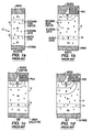
- Figures 1a-d show vertical cross-sections of various semiconductor devices of the prior art illustrating the distribution of recombination centers throughout the silicon substrate.
- Figures 2a-d show vertical cross-sections of various semiconductor devices illustrating the layer of recombination centers in embodiments of the present invention.
- Figure 3 is a pictorial depiction of two wafers to be bonded illustrating misalignment of crystalline features of the two wafers in an embodiment of the present invention.
- a method of controlling minority carrier lifetime in a semiconductor device may include the step of controlling a density of recombination centers (x) at a wafer-to-wafer bonding interface 20 adjacent a blocking layer 22 of the semiconductor device so that the recombination centers are concentrated in a buffer layer 24 at or near bonding interface 20 and adjacent blocking layer 22.
- the density of recombination centers (x) in the buffer layer 24 is in a range of from 10 14 /cm 3 to 10 19 /cm 3 .
- the buffer layer 24 be from 1 micron to 50 microns in thickness.
- the recombination centers (x) are substantially absent from the blocking layer 22 and, typically may be in a concentration of less than the concentration of the buffer layer in the blocking layer 22.
- the figures show bonding interface 20 inside buffer layer 24, although bonding interface 20 may be at an edge or even slightly spaced from buffer layer 24.
- the bonding surface of at least one of two wafers which are to be bonded to form substrate 12 is processed before bonding so that dislocations will form at the wafer-to-wafer bonding interface when the wafers are bonded.
- the dislocations become recombination centers for the minority carriers.
- the bonding surface may be processed before bonding by either or both of the two methods discussed below.
- dislocation refers to any strain location regardless of the cause of the strain ( e . g ., dopant or crystalline misalignment).
- Figure 3 illustrates one way to process the bonding surfaces is to purposely misalign corresponding features at the bonding surfaces 30 so that when the two wafers 32 are bonded the features are misaligned thereby creating dislocations at the wafer-to-wafer bonding interface.
- one of the wafers may be rotated relative to the other so that crystalline axes of the two wafers are not aligned.
- these axes are highly exaggerated by the misaligned lines 34 on the facing bonding surfaces 30.
- one of the bonding surfaces 30 is polished off-axis relative to the other bonding surface. Lines 34 in Figure 3 are also illustrative of the polishing striations resulting from off-axis polishing.
- the features of the either of these methods (that is, the crystal axes and the polishing striations) generate dislocations when wafers 32 are bonded.
- the dislocations are at the wafer-to-wafer bonding interface on both bonding surfaces 30 so that buffer layer 24 is formed with the bonding interface therein.
- the amount by which wafers 32 are misaligned determines the dislocation density in buffer layer 24.
- the misalignment between wafers 32 illustrated in Figure 3 is in a range of from one to 45 degrees of the lines 34 of one wafer 32 relative to the other.
- the greater the misalignment the higher the density of recombination centers.
- the density and distribution of these recombination centers may be modified by appropriate heat treatments, such as a furnace operation or rapid thermal annealing, after bonding.
- Another method of controlling the density of recombination centers is to dope one or both of the bonding surfaces with a suitable dopant or dopants.
- a suitable dopant or dopants are, for example, Au, PT, PD, AG, Cu, Fe, Ni, Co.
- dopants may be evaporated onto or implanted into one or both of the bonding surfaces after polishing and before bonding the two wafers.
- the lower bonding surface (the one on the wafer which does not have blocking layer 22 therein) may be doped with a suitable metal dopant prior to polishing and bonding, and using conventional high temperature treatments to distribute the dopants in what will become buffer layer 24 and establish the desired concentration.
- the dopant concentration in the buffer layer 24 is in a range from 10 14 /cm 3 to 10 19 /cm 3 , depending on the speed required.
- These doping methods is used with the wafers purposely misaligned by a controlled amount to provide a combination of sources of recombination centers.
- the dopant may be selected to provide optimum switching performance (if this is desired) without regard for its solubility or diffusion coefficient.
- the dopant was typically a heavy metal evaporated on to one surface of the wafer which was then heated to 800° to 900°C at which the solid solubility of the metal produced an appropriate concentration of recombination centers.
- the metal had to have an appropriately high diffusion rate so that it could diffuse into the wafer in an acceptable time at this temperature.
- Gold and platinum were typically used because they provided the appropriate combination of energy level, solid solubility and diffusion coefficient to allow the prior art processes to work. Other metals did not meet the needed combination of characteristics.
- the dopant when the dopant is applied just prior to bonding, almost any dopant can be used and may be chosen based on energy level alone.
- the dopants do not move far from the wafer-to-wafer bonding interface because the subsequent bonding temperatures are low enough to not cause any appreciable diffusion.
- suitable heat treatments may be used.
- references to bonding herein are intended to refer generally to any conventional bonding technique, and particularly to the above-mentioned wafer bonding method in which the bonding surfaces of two silicon wafers are polished sufficiently flat so that when the polished surfaces are brought into contact with each other, enough of the neighboring silicon atoms can form covalent bonds across the wafer-to-wafer bonding interface to link the two wafers into a single crystal.
- a method of controlling minority carrier lifetime in a semiconductor device in which the density of recombination centers is controlled so that the recombination centers are concentrated in a thin buffer layer adjacent a blocking layer in one of two bonded wafers.
- the density is controlled by misaligning crystal axes of the two wafers or by doping the bonding surface of one of the wafers before the wafers are bonded. Both methods generate recombination centers in the thin buffer layer that forms around or adjacent the bonding interface.
- a semiconductor device made by this method includes a buffer layer with a significantly higher density of recombination centers than the adjacent blocking layer.
Landscapes
- Recrystallisation Techniques (AREA)
- Pressure Welding/Diffusion-Bonding (AREA)
- Crystals, And After-Treatments Of Crystals (AREA)
- Testing Or Measuring Of Semiconductors Or The Like (AREA)
Claims (7)
- Procédé pour contrôler la durée de vie de porteurs minoritaires dans un dispositif semiconducteur à tranches liées, comprenant les étapes suivantes :prévoir des première et deuxième tranches (32), chaque tranche comportant une surface de liaison (30), chaque tranche comportant au moins une couche fortement dopée, et une des tranches comportant une couche de blocage faiblement dopée (22) en tant que couche de liaison, la couche de blocage faiblement dopée (22) étant placée directement sur la couche fortement dopée de la tranche ; caractérisé parun polissage, avant la liaison, d'une des surfaces de liaison (30) avec un décalage axial par rapport à l'autre surface de liaison pour produire, lorsque les tranches (32) sont liées, des dislocations au niveau de l'interface de liaison de tranche à tranche (20) sur les deux surfaces de liaison (30) de sorte qu'une couche tampon (24) est formée avec l'interface de liaison à l'intérieur ;
le dopage d'une des surfaces de liaison (30) dans ce qui va devenir la couche tampon (24) ; et
la liaison des tranches (32) entre elles au niveau de leurs surfaces de liaison (30) pour créer des centres de recombinaison pour des porteurs minoritaires dans la couche tampon (24). - Procédé selon la revendication 1, dans lequel l'étape de polissage avec décalage axial provoque des stries de polissage dans la surface de liaison (30).
- Procédé selon la revendication 2, comprenant en outre l'évaporation d'un dopant sur une surface de liaison (30).
- Procédé selon la revendication 2, dans lequel l'étape de dopage comprend l'étape consistant à implanter des dopants métalliques dans la tranche (32) ne comportant pas la couche de blocage (22) puis à chauffer pour répartir les dopants métalliques.
- Procédé selon la revendication 2, dans lequel l'implant est un métal choisi dans le groupe comprenant Au, Pt, Pd, Ag, Cu, Fe, Ni et Co.
- Procédé selon la revendication 1, dans lequel la concentration du dopant dans la couche tampon (24) est comprise entre 1014/cm3 et 1019/cm3 et la densité des centres de recombinaison concentrés dans la couche tampon (24) est comprise entre 1014/cm3 et 1019/cm3 et l'épaisseur de la couche tampon (24) est comprise entre 1 micromètre et 50 micromètres.
- Procédé selon la revendication 2, dans lequel les stries de l'une des tranches sont orientées par rapport aux stries de l'autre tranche avec un angle compris entre un et quarante cinq degrés.
Applications Claiming Priority (2)
| Application Number | Priority Date | Filing Date | Title |
|---|---|---|---|
| US08/885,878 US6054369A (en) | 1997-06-30 | 1997-06-30 | Lifetime control for semiconductor devices |
| US885878 | 1997-06-30 |
Publications (3)
| Publication Number | Publication Date |
|---|---|
| EP0889509A2 EP0889509A2 (fr) | 1999-01-07 |
| EP0889509A3 EP0889509A3 (fr) | 1999-11-17 |
| EP0889509B1 true EP0889509B1 (fr) | 2009-05-20 |
Family
ID=25387886
Family Applications (1)
| Application Number | Title | Priority Date | Filing Date |
|---|---|---|---|
| EP98111147A Expired - Lifetime EP0889509B1 (fr) | 1997-06-30 | 1998-06-17 | Contrôle de la durée de vie pour des dispositifs semi-conducteurs |
Country Status (5)
| Country | Link |
|---|---|
| US (1) | US6054369A (fr) |
| EP (1) | EP0889509B1 (fr) |
| JP (1) | JPH1140633A (fr) |
| KR (1) | KR100720675B1 (fr) |
| DE (1) | DE69840843D1 (fr) |
Cited By (1)
| Publication number | Priority date | Publication date | Assignee | Title |
|---|---|---|---|---|
| CN103518252A (zh) * | 2011-05-05 | 2014-01-15 | Abb技术有限公司 | 双极穿通半导体器件和用于制造这样的半导体器件的方法 |
Families Citing this family (45)
| Publication number | Priority date | Publication date | Assignee | Title |
|---|---|---|---|---|
| EP0913872A1 (fr) * | 1997-10-29 | 1999-05-06 | Motorola Semiconducteurs S.A. | Transistor bipolaire à grille isolée |
| FR2773261B1 (fr) | 1997-12-30 | 2000-01-28 | Commissariat Energie Atomique | Procede pour le transfert d'un film mince comportant une etape de creation d'inclusions |
| US5888838A (en) * | 1998-06-04 | 1999-03-30 | International Business Machines Corporation | Method and apparatus for preventing chip breakage during semiconductor manufacturing using wafer grinding striation information |
| US6984571B1 (en) * | 1999-10-01 | 2006-01-10 | Ziptronix, Inc. | Three dimensional device integration method and integrated device |
| DE10003703B4 (de) * | 2000-01-28 | 2007-07-12 | Infineon Technologies Ag | Steuerbares, auf einem Isolationsmaterial gebildetes Halbleiterschaltelement |
| DE10014659C2 (de) * | 2000-03-24 | 2002-08-01 | Infineon Technologies Ag | Halbleiterschaltungsanordnung und entsprechende Herstellungsverfahren |
| US7332750B1 (en) * | 2000-09-01 | 2008-02-19 | Fairchild Semiconductor Corporation | Power semiconductor device with improved unclamped inductive switching capability and process for forming same |
| DE10048437A1 (de) * | 2000-09-29 | 2002-04-18 | Eupec Gmbh & Co Kg | Verfahren zum Herstellen eines Körpers aus Halbleitermaterial mit reduzierter mittlerer freier Weglänge und mit dem Verfahren hergestellter Körper |
| US6538284B1 (en) | 2001-02-02 | 2003-03-25 | Advanced Micro Devices, Inc. | SOI device with body recombination region, and method |
| FR2823596B1 (fr) | 2001-04-13 | 2004-08-20 | Commissariat Energie Atomique | Substrat ou structure demontable et procede de realisation |
| FR2823599B1 (fr) | 2001-04-13 | 2004-12-17 | Commissariat Energie Atomique | Substrat demomtable a tenue mecanique controlee et procede de realisation |
| DE10217610B4 (de) * | 2002-04-19 | 2005-11-03 | Infineon Technologies Ag | Metall-Halbleiter-Kontakt, Halbleiterbauelement, integrierte Schaltungsanordnung und Verfahren |
| FR2842021B1 (fr) * | 2002-07-05 | 2005-05-13 | Commissariat Energie Atomique | Dispositif electronique, notamment dispositif de puissance, a couche mince, et procede de fabrication de ce dispositif |
| FR2848336B1 (fr) | 2002-12-09 | 2005-10-28 | Commissariat Energie Atomique | Procede de realisation d'une structure contrainte destinee a etre dissociee |
| FR2850487B1 (fr) | 2002-12-24 | 2005-12-09 | Commissariat Energie Atomique | Procede de realisation de substrats mixtes et structure ainsi obtenue |
| US7109092B2 (en) | 2003-05-19 | 2006-09-19 | Ziptronix, Inc. | Method of room temperature covalent bonding |
| FR2856844B1 (fr) | 2003-06-24 | 2006-02-17 | Commissariat Energie Atomique | Circuit integre sur puce de hautes performances |
| FR2857953B1 (fr) | 2003-07-21 | 2006-01-13 | Commissariat Energie Atomique | Structure empilee, et procede pour la fabriquer |
| FR2861497B1 (fr) | 2003-10-28 | 2006-02-10 | Soitec Silicon On Insulator | Procede de transfert catastrophique d'une couche fine apres co-implantation |
| FR2864336B1 (fr) * | 2003-12-23 | 2006-04-28 | Commissariat Energie Atomique | Procede de scellement de deux plaques avec formation d'un contact ohmique entre celles-ci |
| DE102005009000B4 (de) * | 2005-02-28 | 2009-04-02 | Infineon Technologies Austria Ag | Vertikales Halbleiterbauelement vom Grabenstrukturtyp und Herstellungsverfahren |
| FR2889887B1 (fr) | 2005-08-16 | 2007-11-09 | Commissariat Energie Atomique | Procede de report d'une couche mince sur un support |
| FR2891281B1 (fr) | 2005-09-28 | 2007-12-28 | Commissariat Energie Atomique | Procede de fabrication d'un element en couches minces. |
| JP2007103770A (ja) * | 2005-10-06 | 2007-04-19 | Sanken Electric Co Ltd | 絶縁ゲート型バイポーラトランジスタ |
| US20080012087A1 (en) * | 2006-04-19 | 2008-01-17 | Henri Dautet | Bonded wafer avalanche photodiode and method for manufacturing same |
| DE102006028718B4 (de) * | 2006-06-20 | 2008-11-13 | Infineon Technologies Ag | Verfahren zur Vereinzelung von Halbleiterwafern zu Halbleiterchips |
| FR2910179B1 (fr) | 2006-12-19 | 2009-03-13 | Commissariat Energie Atomique | PROCEDE DE FABRICATION DE COUCHES MINCES DE GaN PAR IMPLANTATION ET RECYCLAGE D'UN SUBSTRAT DE DEPART |
| DE102007036147B4 (de) * | 2007-08-02 | 2017-12-21 | Infineon Technologies Austria Ag | Verfahren zum Herstellen eines Halbleiterkörpers mit einer Rekombinationszone |
| FR2925221B1 (fr) | 2007-12-17 | 2010-02-19 | Commissariat Energie Atomique | Procede de transfert d'une couche mince |
| FR2947098A1 (fr) | 2009-06-18 | 2010-12-24 | Commissariat Energie Atomique | Procede de transfert d'une couche mince sur un substrat cible ayant un coefficient de dilatation thermique different de celui de la couche mince |
| US9396947B2 (en) | 2011-08-25 | 2016-07-19 | Aeroflex Colorado Springs Inc. | Wafer structure for electronic integrated circuit manufacturing |
| US9312133B2 (en) | 2011-08-25 | 2016-04-12 | Aeroflex Colorado Springs Inc. | Wafer structure for electronic integrated circuit manufacturing |
| US9378955B2 (en) | 2011-08-25 | 2016-06-28 | Aeroflex Colorado Springs Inc. | Wafer structure for electronic integrated circuit manufacturing |
| WO2013028983A1 (fr) * | 2011-08-25 | 2013-02-28 | Aeroflex Colorado Springs Inc. | Structure de tranche pour la fabrication de circuits intégrés électroniques |
| US9378956B2 (en) | 2011-08-25 | 2016-06-28 | Aeroflex Colorado Springs Inc. | Wafer structure for electronic integrated circuit manufacturing |
| CN103700712B (zh) * | 2012-09-27 | 2017-05-03 | 比亚迪股份有限公司 | 一种快恢复二极管的结构及其制造方法 |
| CN103578978B (zh) * | 2013-10-17 | 2016-05-18 | 北京时代民芯科技有限公司 | 一种基于硅基键合材料的高压快恢复二极管制造方法 |
| CN104701162A (zh) * | 2013-12-06 | 2015-06-10 | 江苏物联网研究发展中心 | 半导体器件、pin二极管和igbt的制作方法 |
| DE102017002935A1 (de) | 2017-03-24 | 2018-09-27 | 3-5 Power Electronics GmbH | III-V-Halbleiterdiode |
| JP6911453B2 (ja) * | 2017-03-28 | 2021-07-28 | 富士電機株式会社 | 半導体装置およびその製造方法 |
| DE102018002895A1 (de) | 2018-04-09 | 2019-10-10 | 3-5 Power Electronics GmbH | Stapelförmiges III-V-Halbleiterbauelement |
| CN111463119A (zh) * | 2020-03-11 | 2020-07-28 | 无锡格能微电子有限公司 | 一种重金属Au掺杂工艺 |
| WO2022094587A1 (fr) | 2020-10-29 | 2022-05-05 | Invensas Bonding Technologies, Inc. | Procédés et structures de liaison directe |
| CN115799067A (zh) * | 2023-02-07 | 2023-03-14 | 深圳市威兆半导体股份有限公司 | 高压快恢复二极管的制备方法 |
| CN116031149A (zh) * | 2023-02-07 | 2023-04-28 | 深圳市威兆半导体股份有限公司 | 快恢复二极管的制备方法 |
Family Cites Families (17)
| Publication number | Priority date | Publication date | Assignee | Title |
|---|---|---|---|---|
| US4203780A (en) * | 1978-08-23 | 1980-05-20 | Sony Corporation | Fe Ion implantation into semiconductor substrate for reduced lifetime sensitivity to temperature |
| JPH0770476B2 (ja) * | 1985-02-08 | 1995-07-31 | 株式会社東芝 | 半導体装置の製造方法 |
| US4684413A (en) * | 1985-10-07 | 1987-08-04 | Rca Corporation | Method for increasing the switching speed of a semiconductor device by neutron irradiation |
| JP2633536B2 (ja) * | 1986-11-05 | 1997-07-23 | 株式会社東芝 | 接合型半導体基板の製造方法 |
| US4774196A (en) * | 1987-08-25 | 1988-09-27 | Siliconix Incorporated | Method of bonding semiconductor wafers |
| JPH07107935B2 (ja) * | 1988-02-04 | 1995-11-15 | 株式会社東芝 | 半導体装置 |
| US5231045A (en) * | 1988-12-08 | 1993-07-27 | Fujitsu Limited | Method of producing semiconductor-on-insulator structure by besol process with charged insulating layers |
| JPH0719739B2 (ja) * | 1990-09-10 | 1995-03-06 | 信越半導体株式会社 | 接合ウェーハの製造方法 |
| DE4036222A1 (de) * | 1990-11-14 | 1992-05-21 | Bosch Gmbh Robert | Verfahren zur herstellung von halbleiterelementen, insbesondere von dioden |
| US5451547A (en) * | 1991-08-26 | 1995-09-19 | Nippondenso Co., Ltd. | Method of manufacturing semiconductor substrate |
| FR2681472B1 (fr) * | 1991-09-18 | 1993-10-29 | Commissariat Energie Atomique | Procede de fabrication de films minces de materiau semiconducteur. |
| JP3192000B2 (ja) * | 1992-08-25 | 2001-07-23 | キヤノン株式会社 | 半導体基板及びその作製方法 |
| US5360752A (en) * | 1993-10-28 | 1994-11-01 | Loral Federal Systems Company | Method to radiation harden the buried oxide in silicon-on-insulator structures |
| US5466951A (en) * | 1993-12-08 | 1995-11-14 | Siemens Aktiengesellschaft | Controllable power semiconductor element with buffer zone and method for the manufacture thereof |
| TW289837B (fr) * | 1994-01-18 | 1996-11-01 | Hwelett Packard Co | |
| JPH0837286A (ja) * | 1994-07-21 | 1996-02-06 | Toshiba Microelectron Corp | 半導体基板および半導体基板の製造方法 |
| US5541122A (en) * | 1995-04-03 | 1996-07-30 | Motorola Inc. | Method of fabricating an insulated-gate bipolar transistor |
-
1997
- 1997-06-30 US US08/885,878 patent/US6054369A/en not_active Expired - Fee Related
-
1998
- 1998-06-17 DE DE69840843T patent/DE69840843D1/de not_active Expired - Fee Related
- 1998-06-17 EP EP98111147A patent/EP0889509B1/fr not_active Expired - Lifetime
- 1998-06-29 JP JP10196508A patent/JPH1140633A/ja active Pending
- 1998-06-30 KR KR1019980025616A patent/KR100720675B1/ko not_active Expired - Fee Related
Cited By (2)
| Publication number | Priority date | Publication date | Assignee | Title |
|---|---|---|---|---|
| CN103518252A (zh) * | 2011-05-05 | 2014-01-15 | Abb技术有限公司 | 双极穿通半导体器件和用于制造这样的半导体器件的方法 |
| CN103518252B (zh) * | 2011-05-05 | 2016-03-09 | Abb技术有限公司 | 双极穿通半导体器件和用于制造这样的半导体器件的方法 |
Also Published As
| Publication number | Publication date |
|---|---|
| EP0889509A3 (fr) | 1999-11-17 |
| KR100720675B1 (ko) | 2007-11-12 |
| KR19990007489A (ko) | 1999-01-25 |
| EP0889509A2 (fr) | 1999-01-07 |
| US6054369A (en) | 2000-04-25 |
| DE69840843D1 (de) | 2009-07-02 |
| JPH1140633A (ja) | 1999-02-12 |
Similar Documents
| Publication | Publication Date | Title |
|---|---|---|
| EP0889509B1 (fr) | Contrôle de la durée de vie pour des dispositifs semi-conducteurs | |
| EP0165971B1 (fr) | Procede de fabrication d'un transistor de jonction bipolaire | |
| US5023696A (en) | Semiconductor device having composite substrate formed by fixing two semiconductor substrates in close contact with each other | |
| CN101405847B (zh) | 处理含氧半导体晶片的方法及半导体元件 | |
| US7605052B2 (en) | Method of forming an integrated circuit having a device wafer with a diffused doped backside layer | |
| US6762097B2 (en) | Semiconductor device and method for manufacturing the same | |
| JP3684962B2 (ja) | 半導体装置の製造方法 | |
| US20110042791A1 (en) | Method for treating an oxygen-containing semiconductor wafer, and semiconductor component | |
| US5541122A (en) | Method of fabricating an insulated-gate bipolar transistor | |
| KR20050035175A (ko) | 수직형 소자용 배면 오믹 콘택의 저온 형성 방법 | |
| US20020127783A1 (en) | Method for manufacturing a semiconductor device | |
| JPH11503572A (ja) | SiCの半導体層を有する半導体デバイスを製造する方法 | |
| JP2011151428A (ja) | 裏面オーミックコンタクトを備えた縦型の半導体デバイス | |
| US6909119B2 (en) | Low temperature formation of backside ohmic contacts for vertical devices | |
| EP0200059B1 (fr) | Procédé pour la formation d'un contact ohmique sur un semi-conducteur composé III-V et produit de fabrication semi-conducteur intermédiaire | |
| US4717588A (en) | Metal redistribution by rapid thermal processing | |
| JP4000927B2 (ja) | 半導体装置およびその製造方法 | |
| US20230125859A1 (en) | Method of manufacturing a semiconductor device including ion implantation and semiconductor device | |
| JP4029466B2 (ja) | 炭化けい素半導体素子の製造方法 | |
| JPH09153466A (ja) | 半導体デバイスのキャリアの蓄積を減少させる方法 | |
| JPH07321304A (ja) | 絶縁ゲートバイポーラトランジスタおよびその製造方法 |
Legal Events
| Date | Code | Title | Description |
|---|---|---|---|
| PUAI | Public reference made under article 153(3) epc to a published international application that has entered the european phase |
Free format text: ORIGINAL CODE: 0009012 |
|
| AK | Designated contracting states |
Kind code of ref document: A2 Designated state(s): DE FR GB IT |
|
| AX | Request for extension of the european patent |
Free format text: AL;LT;LV;MK;RO;SI |
|
| PUAL | Search report despatched |
Free format text: ORIGINAL CODE: 0009013 |
|
| AK | Designated contracting states |
Kind code of ref document: A3 Designated state(s): AT BE CH CY DE DK ES FI FR GB GR IE IT LI LU MC NL PT SE |
|
| AX | Request for extension of the european patent |
Free format text: AL;LT;LV;MK;RO;SI |
|
| 17P | Request for examination filed |
Effective date: 20000509 |
|
| AKX | Designation fees paid |
Free format text: DE FR GB IT |
|
| 17Q | First examination report despatched |
Effective date: 20040130 |
|
| GRAP | Despatch of communication of intention to grant a patent |
Free format text: ORIGINAL CODE: EPIDOSNIGR1 |
|
| GRAS | Grant fee paid |
Free format text: ORIGINAL CODE: EPIDOSNIGR3 |
|
| RAP1 | Party data changed (applicant data changed or rights of an application transferred) |
Owner name: INTERSIL CORPORATION |
|
| RAP1 | Party data changed (applicant data changed or rights of an application transferred) |
Owner name: FAIRCHILD SEMICONDUCTOR CORPORATION |
|
| GRAA | (expected) grant |
Free format text: ORIGINAL CODE: 0009210 |
|
| AK | Designated contracting states |
Kind code of ref document: B1 Designated state(s): DE FR GB IT |
|
| REG | Reference to a national code |
Ref country code: GB Ref legal event code: FG4D |
|
| REF | Corresponds to: |
Ref document number: 69840843 Country of ref document: DE Date of ref document: 20090702 Kind code of ref document: P |
|
| PLBE | No opposition filed within time limit |
Free format text: ORIGINAL CODE: 0009261 |
|
| REG | Reference to a national code |
Ref country code: FR Ref legal event code: ST Effective date: 20100226 |
|
| STAA | Information on the status of an ep patent application or granted ep patent |
Free format text: STATUS: NO OPPOSITION FILED WITHIN TIME LIMIT |
|
| 26N | No opposition filed |
Effective date: 20100223 |
|
| GBPC | Gb: european patent ceased through non-payment of renewal fee |
Effective date: 20090820 |
|
| PG25 | Lapsed in a contracting state [announced via postgrant information from national office to epo] |
Ref country code: FR Free format text: LAPSE BECAUSE OF NON-PAYMENT OF DUE FEES Effective date: 20090720 |
|
| PG25 | Lapsed in a contracting state [announced via postgrant information from national office to epo] |
Ref country code: DE Free format text: LAPSE BECAUSE OF NON-PAYMENT OF DUE FEES Effective date: 20100101 |
|
| PG25 | Lapsed in a contracting state [announced via postgrant information from national office to epo] |
Ref country code: GB Free format text: LAPSE BECAUSE OF NON-PAYMENT OF DUE FEES Effective date: 20090820 |
|
| PG25 | Lapsed in a contracting state [announced via postgrant information from national office to epo] |
Ref country code: IT Free format text: LAPSE BECAUSE OF FAILURE TO SUBMIT A TRANSLATION OF THE DESCRIPTION OR TO PAY THE FEE WITHIN THE PRESCRIBED TIME-LIMIT Effective date: 20090520 |