EP0890902A2 - Circuit de redondance pour mémoire à semi-conducteurs - Google Patents
Circuit de redondance pour mémoire à semi-conducteurs Download PDFInfo
- Publication number
- EP0890902A2 EP0890902A2 EP98112767A EP98112767A EP0890902A2 EP 0890902 A2 EP0890902 A2 EP 0890902A2 EP 98112767 A EP98112767 A EP 98112767A EP 98112767 A EP98112767 A EP 98112767A EP 0890902 A2 EP0890902 A2 EP 0890902A2
- Authority
- EP
- European Patent Office
- Prior art keywords
- segment
- word line
- selection signal
- redundancy
- rpdz
- Prior art date
- Legal status (The legal status is an assumption and is not a legal conclusion. Google has not performed a legal analysis and makes no representation as to the accuracy of the status listed.)
- Withdrawn
Links
Images
Classifications
-
- G—PHYSICS
- G11—INFORMATION STORAGE
- G11C—STATIC STORES
- G11C29/00—Checking stores for correct operation ; Subsequent repair; Testing stores during standby or offline operation
-
- G—PHYSICS
- G11—INFORMATION STORAGE
- G11C—STATIC STORES
- G11C29/00—Checking stores for correct operation ; Subsequent repair; Testing stores during standby or offline operation
- G11C29/70—Masking faults in memories by using spares or by reconfiguring
- G11C29/78—Masking faults in memories by using spares or by reconfiguring using programmable devices
- G11C29/785—Masking faults in memories by using spares or by reconfiguring using programmable devices with redundancy programming schemes
-
- G—PHYSICS
- G11—INFORMATION STORAGE
- G11C—STATIC STORES
- G11C29/00—Checking stores for correct operation ; Subsequent repair; Testing stores during standby or offline operation
- G11C29/70—Masking faults in memories by using spares or by reconfiguring
- G11C29/78—Masking faults in memories by using spares or by reconfiguring using programmable devices
- G11C29/80—Masking faults in memories by using spares or by reconfiguring using programmable devices with improved layout
- G11C29/808—Masking faults in memories by using spares or by reconfiguring using programmable devices with improved layout using a flexible replacement scheme
-
- G—PHYSICS
- G11—INFORMATION STORAGE
- G11C—STATIC STORES
- G11C29/00—Checking stores for correct operation ; Subsequent repair; Testing stores during standby or offline operation
- G11C29/70—Masking faults in memories by using spares or by reconfiguring
- G11C29/78—Masking faults in memories by using spares or by reconfiguring using programmable devices
- G11C29/84—Masking faults in memories by using spares or by reconfiguring using programmable devices with improved access time or stability
Definitions
- the present invention relates to a redundancy circuit for semiconductor memories with word lines organized in segments, when a defective word line occurs assigned in a segment by means of the respective segments Fuse sets a redundant due to inter-segment redundancy Word line in the same or in a different segment a segment selection signal can be activated.
- the word lines are usually in Organized segments. With so-called inter-segment redundancy can be redundant if a defective word line occurs Word lines both from the same segment, in which is the defective word line, as well as from neighboring Segments used to make this broken word line to replace.
- a problem with inter-segment redundancy lies in the fact that, if necessary, the activation of the segment prevented with the defective word line and instead the segment is to be activated in which the redundant word line is located. This may be the case also be the segment with the defective word line if in this segment also has the redundant word line.
- the redundancy circuit according to the invention thus converts the output signals of the fuse sets directly, i.e. without the help of Row addresses, in segment selection signals, so that no logical Linking the fuse output signals with the Address information is necessary and a logic level is saved can be. This will increase the access time despite the flexible inter-segment redundancy is not increased, and that too activating segment can by the directly from the fuse output signal generated segment selection signal decoded very quickly become.
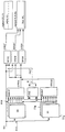
- two blocks 10, 11 are shown, each consisting of eight fuse sets for segments "000” to "111", each fuse set comprising ten fuses and a master fuse.
- the master fuse is used to activate the redundancy and to switch on the corresponding block.
- a fuse set 11 1 is assigned for fuses for "000”
- a fuse set 11 8 is provided for fuses for "111”.
- Row addresses RA are located at the input of the redundancy circuit or RA1, ..., RA10, which are supplied to the blocks 10, 11.
- the Row address RA becomes a segment selection signal block RPDZ and a word line selection signal block RPDW, which a segment selection signal RPDZ 'or a word line selection signal Generate RPDW '.
- the segment to be activated for example, a segment "segment 8, 9, 10", by the Segment selection signal RPDZ 'selected, which from the row addresses RA8, RA9, RA10 is generated.
- Which word line WL "segment 8, 9, 10" is activated within this segment is determined by the signal RPDW 'which consists of the addresses RA0, ..., RA7 is derived.
- the row decoders are initially located the signals RPDW ', ie the signals for selecting a word line within the activated segment. Right away then one of the segment selection signals RPDZ 'becomes active, so that the activation of the corresponding word line WL begin can.
- the signals FFR0A or FFR1A "high” if an address is detected. They switch over the segment selection signal block RPDZ or via the word line selection signal block RPDW the signal RPDZ 'for selection of the segment with the defective word line or the signal RPDW 'to select the word line "defect WL” and enter the redundant word line "Red. WL” via a block RPDR using a signal RPDR 'free.
- the RPDR 'signal selects thus the redundant word line in the segment "segment 8r, 9r, 10r ".
- the segment selection signal RPDZ ' is generated by the output signals FRX of blocks 10, 11 are evaluated, as already explained above: Is the created one correct? Row address RA, for example, with the fused address of the the fuse sets assigned to the segment "segment 8r, 9r, 10r" match, a signal FRZ 'is activated in the circuit FRZ, which corresponds to the address 8r, 9r, 10r.
- This signal FRZ 'therefore selects a segment for redundancy and overwrites it in the segment selection signal block RPDZ that regularly selected signal. For example, it is high if there is no redundancy and low if redundancy occurs.
- the Signal FRZ 'is thus supplied to the segment selection signal block RPDZ and overwrites that from the original Line address 8, 9, 10 generated segment selection signal.
Landscapes
- For Increasing The Reliability Of Semiconductor Memories (AREA)
- Dram (AREA)
- Techniques For Improving Reliability Of Storages (AREA)
Applications Claiming Priority (2)
| Application Number | Priority Date | Filing Date | Title |
|---|---|---|---|
| DE19729579A DE19729579C2 (de) | 1997-07-10 | 1997-07-10 | Verfahren zum Aktivieren einer redundanten Wortleitung bei Inter-Segment-Redundanz bei einem Halbleiterspeicher mit in Segmenten organisierten Wortleitungen |
| DE19729579 | 1997-07-10 |
Publications (2)
| Publication Number | Publication Date |
|---|---|
| EP0890902A2 true EP0890902A2 (fr) | 1999-01-13 |
| EP0890902A3 EP0890902A3 (fr) | 1999-09-22 |
Family
ID=7835296
Family Applications (1)
| Application Number | Title | Priority Date | Filing Date |
|---|---|---|---|
| EP98112767A Withdrawn EP0890902A3 (fr) | 1997-07-10 | 1998-07-09 | Circuit de redondance pour mémoire à semi-conducteurs |
Country Status (7)
| Country | Link |
|---|---|
| US (1) | US6188617B1 (fr) |
| EP (1) | EP0890902A3 (fr) |
| JP (1) | JP3660804B2 (fr) |
| KR (1) | KR100325649B1 (fr) |
| CN (1) | CN1269132C (fr) |
| DE (1) | DE19729579C2 (fr) |
| TW (1) | TW394955B (fr) |
Families Citing this family (3)
| Publication number | Priority date | Publication date | Assignee | Title |
|---|---|---|---|---|
| US6314030B1 (en) * | 2000-06-14 | 2001-11-06 | Micron Technology, Inc. | Semiconductor memory having segmented row repair |
| US7111193B1 (en) * | 2002-07-30 | 2006-09-19 | Taiwan Semiconductor Manufacturing Co. Ltd. | Semiconductor memory having re-configurable fuse set for redundancy repair |
| US7613060B2 (en) | 2007-05-21 | 2009-11-03 | Micron Technology, Inc. | Methods, circuits, and systems to select memory regions |
Family Cites Families (6)
| Publication number | Priority date | Publication date | Assignee | Title |
|---|---|---|---|---|
| US4754434A (en) * | 1985-08-28 | 1988-06-28 | Advanced Micro Devices, Inc. | Switching plane redundancy |
| US5126973A (en) * | 1990-02-14 | 1992-06-30 | Texas Instruments Incorporated | Redundancy scheme for eliminating defects in a memory device |
| JP3040625B2 (ja) * | 1992-02-07 | 2000-05-15 | 松下電器産業株式会社 | 半導体記憶装置 |
| WO1993021578A1 (fr) * | 1992-04-16 | 1993-10-28 | Siemens Aktiengesellschaft | Memoire a semi-conducteurs integre a redondance |
| KR950004623B1 (ko) * | 1992-12-07 | 1995-05-03 | 삼성전자주식회사 | 리던던시 효율이 향상되는 반도체 메모리 장치 |
| KR100192574B1 (ko) * | 1995-10-04 | 1999-06-15 | 윤종용 | 디코디드 퓨즈를 사용한 반도체 메모리 장치의 컬럼 리던던시 회로 |
-
1997
- 1997-07-10 DE DE19729579A patent/DE19729579C2/de not_active Expired - Lifetime
-
1998
- 1998-07-06 TW TW087110889A patent/TW394955B/zh not_active IP Right Cessation
- 1998-07-07 JP JP19135398A patent/JP3660804B2/ja not_active Expired - Fee Related
- 1998-07-09 EP EP98112767A patent/EP0890902A3/fr not_active Withdrawn
- 1998-07-10 CN CNB981159516A patent/CN1269132C/zh not_active Expired - Fee Related
- 1998-07-10 KR KR1019980027747A patent/KR100325649B1/ko not_active Expired - Fee Related
- 1998-07-13 US US09/115,618 patent/US6188617B1/en not_active Expired - Lifetime
Also Published As
| Publication number | Publication date |
|---|---|
| US6188617B1 (en) | 2001-02-13 |
| EP0890902A3 (fr) | 1999-09-22 |
| KR19990013743A (ko) | 1999-02-25 |
| CN1205520A (zh) | 1999-01-20 |
| DE19729579C2 (de) | 2000-12-07 |
| KR100325649B1 (ko) | 2002-05-09 |
| JPH1173795A (ja) | 1999-03-16 |
| JP3660804B2 (ja) | 2005-06-15 |
| DE19729579A1 (de) | 1999-01-14 |
| TW394955B (en) | 2000-06-21 |
| CN1269132C (zh) | 2006-08-09 |
Similar Documents
| Publication | Publication Date | Title |
|---|---|---|
| DE19851861B4 (de) | Fehleranalysespeicher für Halbleiterspeicher-Testvorrichtungen und Speicherverfahren unter Verwendung des Fehleranalysespeichers | |
| DE19640437B4 (de) | Spaltenredundanzschaltkreis | |
| DE3886668T2 (de) | Löschbares programmierbares Festwertspeichergerät. | |
| DE4236099C2 (de) | Redundanzspalten-Schaltkreis für eine Halbleiter-Speichervorrichtung | |
| DE69329220T2 (de) | Zeilenredundanzschaltung eines Halbleiterspeichersgeräts | |
| DE4341692C2 (de) | Reihenredundanzschaltkreis für eine Halbleiter-Speichervorrichtung | |
| DE3638632C2 (fr) | ||
| DE4006285C2 (fr) | ||
| DE4328605A1 (de) | Halbleiterspeichereinrichtung | |
| DE3603926A1 (de) | Halbleiter-speicherelement | |
| DE2400064A1 (de) | Speicherpruefanordnung und diese verwendendes endgeraetsystem in einem datenverarbeitungssystem | |
| DE69120301T2 (de) | Speicherprüfgerät | |
| DE19680641C2 (de) | Fehlerspeicher-Analysiervorrichtung in einem Halbleiterspeichertestsystem | |
| DE69520659T2 (de) | Programmierbares Multibitregister für Übereinstimmungs- und Sprungbetrieb, und Übereinstimmungssicherungszelle | |
| DE3827174A1 (de) | Halbleiter-speichervorrichtung | |
| DE19922786B4 (de) | Halbleiterspeicher mit Testeinrichtung | |
| DE69032844T2 (de) | Halbleiterspeicher mit Einrichtung zum Ersetzen defekter Speicherzellen | |
| DE19830362A1 (de) | Halbleiterspeichervorrichtung | |
| EP0890902A2 (fr) | Circuit de redondance pour mémoire à semi-conducteurs | |
| DE10331068A1 (de) | Verfahren zum Auslesen von Fehlerinformationen aus einem integrierten Baustein und integrierter Speicherbaustein | |
| DE19843470A1 (de) | Integrierter Speicher mit Selbstreparaturfunktion | |
| DE10343563A1 (de) | Flashspeicher mit Wortleitungs-Reparaturmöglichkeit | |
| DE19740933C2 (de) | Dynamischer Speicher mit zwei Betriebsarten | |
| EP0453609B1 (fr) | Procédé pour tester la plus petite unité adressable d'un RAM pour détecter des erreurs de bits dépassant un nombre donné | |
| DE4132298A1 (de) | Halbleiterspeicher-redundanz |
Legal Events
| Date | Code | Title | Description |
|---|---|---|---|
| PUAI | Public reference made under article 153(3) epc to a published international application that has entered the european phase |
Free format text: ORIGINAL CODE: 0009012 |
|
| AK | Designated contracting states |
Kind code of ref document: A2 Designated state(s): DE FR GB IE IT NL |
|
| AX | Request for extension of the european patent |
Free format text: AL;LT;LV;MK;RO;SI |
|
| PUAL | Search report despatched |
Free format text: ORIGINAL CODE: 0009013 |
|
| AK | Designated contracting states |
Kind code of ref document: A3 Designated state(s): AT BE CH CY DE DK ES FI FR GB GR IE IT LI LU MC NL PT SE |
|
| AX | Request for extension of the european patent |
Free format text: AL;LT;LV;MK;RO;SI |
|
| 17P | Request for examination filed |
Effective date: 20000121 |
|
| AKX | Designation fees paid |
Free format text: DE FR GB IE IT NL |
|
| RAP1 | Party data changed (applicant data changed or rights of an application transferred) |
Owner name: INFINEON TECHNOLOGIES AG |
|
| 17Q | First examination report despatched |
Effective date: 20010928 |
|
| STAA | Information on the status of an ep patent application or granted ep patent |
Free format text: STATUS: THE APPLICATION IS DEEMED TO BE WITHDRAWN |
|
| 18D | Application deemed to be withdrawn |
Effective date: 20020309 |