EP0890902A2 - Redundancy circuit for semiconductor memory devide - Google Patents
Redundancy circuit for semiconductor memory devide Download PDFInfo
- Publication number
- EP0890902A2 EP0890902A2 EP98112767A EP98112767A EP0890902A2 EP 0890902 A2 EP0890902 A2 EP 0890902A2 EP 98112767 A EP98112767 A EP 98112767A EP 98112767 A EP98112767 A EP 98112767A EP 0890902 A2 EP0890902 A2 EP 0890902A2
- Authority
- EP
- European Patent Office
- Prior art keywords
- segment
- word line
- selection signal
- redundancy
- rpdz
- Prior art date
- Legal status (The legal status is an assumption and is not a legal conclusion. Google has not performed a legal analysis and makes no representation as to the accuracy of the status listed.)
- Withdrawn
Links
Images
Classifications
-
- G—PHYSICS
- G11—INFORMATION STORAGE
- G11C—STATIC STORES
- G11C29/00—Checking stores for correct operation ; Subsequent repair; Testing stores during standby or offline operation
-
- G—PHYSICS
- G11—INFORMATION STORAGE
- G11C—STATIC STORES
- G11C29/00—Checking stores for correct operation ; Subsequent repair; Testing stores during standby or offline operation
- G11C29/70—Masking faults in memories by using spares or by reconfiguring
- G11C29/78—Masking faults in memories by using spares or by reconfiguring using programmable devices
- G11C29/785—Masking faults in memories by using spares or by reconfiguring using programmable devices with redundancy programming schemes
-
- G—PHYSICS
- G11—INFORMATION STORAGE
- G11C—STATIC STORES
- G11C29/00—Checking stores for correct operation ; Subsequent repair; Testing stores during standby or offline operation
- G11C29/70—Masking faults in memories by using spares or by reconfiguring
- G11C29/78—Masking faults in memories by using spares or by reconfiguring using programmable devices
- G11C29/80—Masking faults in memories by using spares or by reconfiguring using programmable devices with improved layout
- G11C29/808—Masking faults in memories by using spares or by reconfiguring using programmable devices with improved layout using a flexible replacement scheme
-
- G—PHYSICS
- G11—INFORMATION STORAGE
- G11C—STATIC STORES
- G11C29/00—Checking stores for correct operation ; Subsequent repair; Testing stores during standby or offline operation
- G11C29/70—Masking faults in memories by using spares or by reconfiguring
- G11C29/78—Masking faults in memories by using spares or by reconfiguring using programmable devices
- G11C29/84—Masking faults in memories by using spares or by reconfiguring using programmable devices with improved access time or stability
Definitions
- the present invention relates to a redundancy circuit for semiconductor memories with word lines organized in segments, when a defective word line occurs assigned in a segment by means of the respective segments Fuse sets a redundant due to inter-segment redundancy Word line in the same or in a different segment a segment selection signal can be activated.
- the word lines are usually in Organized segments. With so-called inter-segment redundancy can be redundant if a defective word line occurs Word lines both from the same segment, in which is the defective word line, as well as from neighboring Segments used to make this broken word line to replace.
- a problem with inter-segment redundancy lies in the fact that, if necessary, the activation of the segment prevented with the defective word line and instead the segment is to be activated in which the redundant word line is located. This may be the case also be the segment with the defective word line if in this segment also has the redundant word line.
- the redundancy circuit according to the invention thus converts the output signals of the fuse sets directly, i.e. without the help of Row addresses, in segment selection signals, so that no logical Linking the fuse output signals with the Address information is necessary and a logic level is saved can be. This will increase the access time despite the flexible inter-segment redundancy is not increased, and that too activating segment can by the directly from the fuse output signal generated segment selection signal decoded very quickly become.
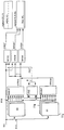
- two blocks 10, 11 are shown, each consisting of eight fuse sets for segments "000” to "111", each fuse set comprising ten fuses and a master fuse.
- the master fuse is used to activate the redundancy and to switch on the corresponding block.
- a fuse set 11 1 is assigned for fuses for "000”
- a fuse set 11 8 is provided for fuses for "111”.
- Row addresses RA are located at the input of the redundancy circuit or RA1, ..., RA10, which are supplied to the blocks 10, 11.
- the Row address RA becomes a segment selection signal block RPDZ and a word line selection signal block RPDW, which a segment selection signal RPDZ 'or a word line selection signal Generate RPDW '.
- the segment to be activated for example, a segment "segment 8, 9, 10", by the Segment selection signal RPDZ 'selected, which from the row addresses RA8, RA9, RA10 is generated.
- Which word line WL "segment 8, 9, 10" is activated within this segment is determined by the signal RPDW 'which consists of the addresses RA0, ..., RA7 is derived.
- the row decoders are initially located the signals RPDW ', ie the signals for selecting a word line within the activated segment. Right away then one of the segment selection signals RPDZ 'becomes active, so that the activation of the corresponding word line WL begin can.
- the signals FFR0A or FFR1A "high” if an address is detected. They switch over the segment selection signal block RPDZ or via the word line selection signal block RPDW the signal RPDZ 'for selection of the segment with the defective word line or the signal RPDW 'to select the word line "defect WL” and enter the redundant word line "Red. WL” via a block RPDR using a signal RPDR 'free.
- the RPDR 'signal selects thus the redundant word line in the segment "segment 8r, 9r, 10r ".
- the segment selection signal RPDZ ' is generated by the output signals FRX of blocks 10, 11 are evaluated, as already explained above: Is the created one correct? Row address RA, for example, with the fused address of the the fuse sets assigned to the segment "segment 8r, 9r, 10r" match, a signal FRZ 'is activated in the circuit FRZ, which corresponds to the address 8r, 9r, 10r.
- This signal FRZ 'therefore selects a segment for redundancy and overwrites it in the segment selection signal block RPDZ that regularly selected signal. For example, it is high if there is no redundancy and low if redundancy occurs.
- the Signal FRZ 'is thus supplied to the segment selection signal block RPDZ and overwrites that from the original Line address 8, 9, 10 generated segment selection signal.
Landscapes
- For Increasing The Reliability Of Semiconductor Memories (AREA)
- Dram (AREA)
- Techniques For Improving Reliability Of Storages (AREA)
Abstract
Die Erfindung betrifft eine Redundanzschaltung für Halbleiterspeicher mit in Segmenten organisierten Wortleitungen (WL), bei der bei Auftreten einer defekten Wortleitung (defect WL) in einem Segment (segment 8, 9, 10) mittels den jeweiligen Segmenten zugeordneten Fuse-Sets (10, 11) durch Inter-Segment-Redundanz eine redundante Wortleitung (Red. WL) im gleichen oder in einem anderen Segment durch ein Segmentauswahlsignal (RPDZ') aktivierbar ist. Das Segmentauswahlsignal (RPDZ') wird durch Auswertung des Ausgangssignals der Fuse-Sets direkt erzeugt. <IMAGE>The invention relates to a redundancy circuit for semiconductor memories with word lines (WL) organized in segments, in which, when a defective word line (defect WL) occurs in a segment (segment 8, 9, 10) by means of fuse sets (10, 11) assigned to the respective segments ) by inter-segment redundancy, a redundant word line (Red. WL) can be activated in the same segment or in another segment by a segment selection signal (RPDZ '). The segment selection signal (RPDZ ') is generated directly by evaluating the output signal of the fuse sets. <IMAGE>
Description
Die vorliegende Erfindung betrifft eine Redundanzschaltung für Halbleiterspeicher mit in Segmenten organisierten Wortleitungen, bei der bei Auftreten einer defekten Wortleitung in einem Segment mittels den jeweiligen Segmenten zugeordneten Fuse-Sets durch Inter-Segment-Redundanz eine redundante Wortleitung im gleichen oder in einem anderen Segment durch ein Segmentauswahlsignal aktivierbar ist.The present invention relates to a redundancy circuit for semiconductor memories with word lines organized in segments, when a defective word line occurs assigned in a segment by means of the respective segments Fuse sets a redundant due to inter-segment redundancy Word line in the same or in a different segment a segment selection signal can be activated.
Bei Halbleiterspeichern sind die Wortleitungen gewöhnlich in Segmenten organisiert. Bei der sogenannten Inter-Segment-Redundanz können bei Auftreten einer defekten Wortleitung redundante Wortleitungen sowohl aus dem gleichen Segment, in welchem die defekte Wortleitung vorliegt, als auch aus benachbarten Segmenten verwendet werden, um diese defekte Wortleitung zu ersetzen.In semiconductor memories, the word lines are usually in Organized segments. With so-called inter-segment redundancy can be redundant if a defective word line occurs Word lines both from the same segment, in which is the defective word line, as well as from neighboring Segments used to make this broken word line to replace.
Ein bei der Inter-Segment-Redundanz auftretendes Problem liegt nun darin, daß gegebenenfalls die Aktivierung des Segments mit der defekten Wortleitung verhindert und statt dessen das Segment aktiviert werden soll, in welchem sich die redundante Wortleitung befindet. Dies kann gegebenenfalls auch das Segment mit der defekten Wortleitung sein, wenn in diesem Segment zusätzlich die redundante Wortleitung vorliegt.A problem with inter-segment redundancy lies in the fact that, if necessary, the activation of the segment prevented with the defective word line and instead the segment is to be activated in which the redundant word line is located. This may be the case also be the segment with the defective word line if in this segment also has the redundant word line.
Um nun keine Zugriffszeit zu verlieren, muß bei einer solchen Redundanzschaltung für Halbleiterspeicher die Dekodierung des Signals, das das zu aktivierende Segment auswählt, also die Dekodierung des Segmentauswahlsignales, sehr rasch erfolgen.In order not to lose any access time, one must Redundancy circuit for semiconductor memory decoding the Signal that selects the segment to be activated, i.e. the Decoding of the segment selection signal is done very quickly.
Bisher werden in bestehenden Redundanzschaltungen durch Auswertung von Fuse-Ausgangssignalen mit Hilfe der ursprünglichen Zeilenadressen Segmentauswahlsignale generiert, welche das Segment mit der redundanten Wortleitung angeben. Es ist hier also eine zusätzliche Logik-Stufe erforderlich, um das Fuse-Ausgangssignal mit der Adreßinformation zu verknüpfen.So far in existing redundancy circuits by evaluation of fuse output signals using the original Row addresses segment selection signals generated which specify the segment with the redundant word line. It is So here an additional logic level is required to do this Link fuse output signal with the address information.
Es ist nun Aufgabe der vorliegenden Erfindung, eine Redundanzschaltung für Halbleiterspeicher zu schaffen, die ohne solche zusätzliche Logik-Stufe die Erzeugung von Segmentauswahlsignalen bei Auftreten defekter Wortleitungen erlaubt.It is an object of the present invention to provide a redundancy circuit for semiconductor memories which allows the generation of segment selection signals when defective word lines occur without such an additional logic stage.
Diese Aufgabe wird bei einer Redundanzschaltung für Halbleiterspeicher der eingangs genannten Art erfindungsgemäß dadurch gelöst, daß das Segmentauswahlsignal durch Auswertung des Ausgangssignals der Fuse-Sets erzeugbar ist. Dies geschieht in vorteilhafter Weise dadurch, daS bei Übereinstimmung einer angelegten Zeilenadresse mit der gefusten Adresse des einem Segment zugeordneten Fuse-Sets eine den Fuse-Sets nachgeordnete Schaltung ein der Adresse dieses Segments zugeordnetes Signal aktiviert, das ein aus der Zeilenadresse erzeugtes Segmentauswahlsignal überschreibt und die redundante Wortleitung aktiviert.This task is accomplished with a redundancy circuit for semiconductor memories of the type mentioned in the introduction solved that the segment selection signal by evaluation the output signal of the fuse sets can be generated. this happens in an advantageous manner in that if there is agreement a line address created with the searched address of the fuse set assigned to a segment is one of the fuse sets downstream circuitry associated with the address of this segment Activated signal that a generated from the row address Segment selection signal overwrites and the redundant Word line activated.
Die erfindungsgemaße Redundanzschaltung wandelt also die Ausgangssignale der Fuse-Sets direkt, d.h. ohne Zuhilfenahme von Zeilenadressen, in Segmentauswahlsignale um, so daS keine logische Verknüpfung von den Fuse-Ausgangssignalen mit der Adreßinformation notwendig ist und eine Logik-Stufe eingespart werden kann. Dadurch wird die Zugriffszeit trotz der flexiblen Inter-Segment-Redundanz nicht erhöht, und das zu aktivierende Segment kann durch das unmittelbar aus dem Fuse-Ausgangssignal erzeugte Segmentauswahlsignal sehr rasch dekodiert werden.The redundancy circuit according to the invention thus converts the output signals of the fuse sets directly, i.e. without the help of Row addresses, in segment selection signals, so that no logical Linking the fuse output signals with the Address information is necessary and a logic level is saved can be. This will increase the access time despite the flexible inter-segment redundancy is not increased, and that too activating segment can by the directly from the fuse output signal generated segment selection signal decoded very quickly become.
Nachfolgend wird die Erfindung anhand der Zeichnung näher erläutert, in deren einziger Figur ein Blockschaltbild der erfindungsgemäßen Redundanzschaltung für Halbleiterspeicher dargestellt ist.The invention is explained in more detail below with reference to the drawing, in their single figure a block diagram of the invention Redundancy circuit for semiconductor memories is shown.
In der Figur sind zunächst zwei Blöcke 10, 11 gezeigt, die
jeweils aus acht Fuse-Sets für Segmente "000" bis "111" bestehen,
wobei jeder Fuse-Set zehn Fuses und eine Masterfuse
umfaßt. Die Masterfuse dient bekanntlich zur Aktivierung der
Redundanz und zur Einschaltung des entsprechenden Blockes.
Beispielsweise ist im Block 11 ein Fuse-Set 111 für Fuses für
"000" zugeordnet, während ein Fuse-Set 118 für Fuses für
"111" vorgesehen ist.In the figure, two
Am Eingang der Redundanzschaltung liegen Zeilenadressen RA
bzw. RA1,...,RA10, die den Blöcken 10, 11 zugeführt sind. Die
Zeilenadresse RA wird einem Segmentauswahlsignalblock RPDZ
und einem Wortleitungsauswahlsignalblock RPDW zugeführt, die
ein Segmentauswahlsignal RPDZ' bzw. ein Wortleitungsauswahl-Signal
RPDW' generieren. Das zu aktivierende Segment, also
beispielsweise ein Segment "segment 8, 9, 10", wird durch das
Segmentauswahlsignal RPDZ' ausgewählt, welches aus den Zeilenadressen
RA8, RA9, RA10 erzeugt ist. Welche Wortleitung WL
innerhalb dieses Segmentes "segment 8, 9, 10" aktiviert wird,
wird durch das Signal RPDW' bestimmt, das aus den Adressen
RA0,...,RA7 abgeleitet ist.Row addresses RA are located at the input of the redundancy circuit
or RA1, ..., RA10, which are supplied to the
An den Zeilendekodern liegen nach einem RAS-Befehl zunächst die Signale RPDW', also die Signale zur Auswahl einer Wortleitung innerhalb des aktivierten Segments, an. Unmittelbar danach wird eines der Segmentauswahlsignale RPDZ' aktiv, so daß die Aktivierung der entsprechenden Wortleitung WL beginnen kann.After a RAS command, the row decoders are initially located the signals RPDW ', ie the signals for selecting a word line within the activated segment. Right away then one of the segment selection signals RPDZ 'becomes active, so that the activation of the corresponding word line WL begin can.
Im Fall einer Inter-Segment-Redundanz kann es nun vorkommen,
daß die redundante Wortleitung "Red. WL" in einem anderen
Segment, also beispielsweise einem Segment "segment 8r, 9r,
10r", als dem durch die Zeilenadressen RA8, RA9, RA10 bestimmten
Segment "segment 8, 9, 10" liegt. In diesem Fall muß
dann ein neues Segmentauswahlsignal RPDZ' generiert werden,
welches die Aktivierung der redundanten Wortleitung "Red. WL"
in dem neuen Segment "segment 8r, 9r, 10r" startet. Gleichzeitig
muß die Aktivierung der adressierten Wortleitung
"defect WL" im Segment "segment 8, 9, 10" verhindert werden.In the case of inter-segment redundancy, it can now happen
that the redundant word line "Red. WL" in another
Segment, for example a segment "
In einem zusammenhängenden Block des Halbleiterspeichers befinden sich beispielsweise acht Segmente, deren redundante Wortleitungen frei genutzt werden können, um defekte Wortleitungen in einem beliebigen Segment dieser acht Segmente mittels der Inter-Segment-Redundanz zu reparieren. Jedem Segment sind dabei genau zwei Fuse-Sets zugeordnet, d.h. es liegen zwei redundante Wortleitungen in jedem Segment vor.Are located in a coherent block of the semiconductor memory for example, eight segments, their redundant Word lines can be used freely to defective word lines in any segment of these eight segments using to repair the inter-segment redundancy. Every segment exactly two fuse sets are assigned, i.e. There are two redundant word lines in each segment.
Stimmt die angelegte Zeilenadresse RA mit einer der gefusten
Adressen überein, liegt also eine defekte Wortleitung "defect
WL" vor, so wird eines der 16 Ausgangssignale FRX der Blöcke
10, 11 der Fuses aktiv. Das bedeutet beispielsweise, daß das
Signal FRX "niedrig" wird, wenn eine gefuste Adresse festgestellt
wird. Die Signale FRX sind Blöcken FRBUF zugeführt,
die als Puffer für die Fuse-Ausgangssignale FRX dienen und in
denen geprüft wird, ob eine redundante Wortleitung "Red. WL"
herangezogen werden muß, was dann der Fall ist, wenn ein Signal
FRX niedrig ist. Die Blöcke FRBUF aktivieren ein Signal
FFR0A bzw. FFR1A, so daß anstelle der ursprünglich adressierten
Wortleitung "defect WL" die redundante Wortleitung "Red.
WL" aktiviert wird. Im einzelnen sind die Signale FFR0A bzw.
FFR1A "hoch", wenn eine Adresse gefust ist. Sie schalten über
den Segmentauswahlsignalblock RPDZ bzw. über den Wortleitungsauswahlsignal-block
RPDW das Signal RPDZ' zur Auswahl
des Segmentes mit der defekten Wortleitung bzw. das Signal
RPDW' zur Auswahl der Wortleitung "defect WL" ab und geben
über einen Block RPDR die redundante Wortleitung "Red. WL"
mit Hilfe eines Signals RPDR' frei. Das Signal RPDR' wählt
also die redundante Wortleitung im Segment "segment 8r, 9r,
10r" aus. Does the row address RA match one of the fuzzed ones
Addresses match, so there is a defective word line "defect
WL "before, one of the 16 output signals FRX of the
Die Erzeugung des Segmentauswahlsignals RPDZ' erfolgt, indem
die Ausgangssignale FRX der Blöcke 10, 11 ausgewertet werden,
wie dies bereits oben erläutert wurde: Stimmt die angelegte
Zeilenadresse RA beispielsweise mit der gefusten Adresse des
dem Segment "segment 8r, 9r, 10r" zugeordneten Fuse-Sets
überein, so wird in der Schaltung FRZ ein Signal FRZ' aktiviert,
welches der Adresse 8r, 9r, 10r entspricht. Dieses Signal
FRZ' wählt also bei Redundanz ein Segment und überschreibt
in dem Segmentauswahlsignalblock RPDZ das regelmäßig
gewählte Signal. Es ist beispielsweise hoch, falls keine Redundanz
vorliegt, und niedrig, falls Redundanz auftritt. Das
Signal FRZ' ist also dem Segmentauswahlsignalblock RPDZ zugeführt
und überschreibt in diesem das aus der ursprünglichen
Zeilenadresse 8, 9, 10 erzeugte Segmentauswahlsignal.The segment selection signal RPDZ 'is generated by
the output signals FRX of
Es wird somit eine redundante Wortleitung "Red. WL" in dem
Segment "segment 8r, 9r, 10r" aktiviert. Welche der beiden in
diesem Segment vorhandenen redundanten Wortleitungen tatsächlich
aktiviert wird, hängt davon ab, in welcher der beiden
Gruppen von Fuse-Sets die Übereinstimmung zwischen angelegter
und gefuster Adresse auftrat, was wiederum durch die Signale
FFR0A bzw. FFR1A bestimmt wird.There is thus a redundant word line "Red. WL" in the
Segment "
Claims (2)
dadurch gekennzeichnet,
daß das Segmentauswahlsignal (RPDZ') durch Auswertung des Ausgangssignals (FRX) der Fuse-Sets (10, 11) erzeugbar ist.Redundancy circuit for semiconductor memories with word lines (WL) organized in segments, in which when a defective word line (defect WL) occurs in a segment (segment 8, 9, 10) by means of fuse sets (10, 11) assigned to the respective segments by inter Segment redundancy a redundant word line (Red. WL) in the same or in another segment (segment 8, 9, 10; segment 8r, 9r, 10r) can be activated by a segment selection signal (RPDZ '),
characterized,
that the segment selection signal (RPDZ ') can be generated by evaluating the output signal (FRX) of the fuse sets (10, 11).
dadurch gekennzeichnet,
daß bei Übereinstimmung einer angelegten Zeilenadresse (RA; RA1,....,RA10) mit der gefusten Adresse des einem Segment zugeordneten Fuse-Sets (10, 11) eine den Fuse-Sets nachgeschaltete Schaltung (FRZ) ein der Adresse dieses Segments zugeordnetes Signal (FRZ') aktiviert wird, das ein aus der Zeilenadresse erzeugtes Segmentauswahlsignal (RPDZ') überschreibt und die redundante Wortleitung (Red. WL) aktiviert.Redundancy circuit according to claim 1,
characterized,
that if a line address (RA; RA1, ...., RA10) matches the fused address of the fuse set (10, 11) assigned to a segment, a circuit (FRZ) connected downstream of the fuse set is assigned to the address of this segment Signal (FRZ ') is activated, which overwrites a segment selection signal (RPDZ') generated from the row address and activates the redundant word line (Red. WL).
Applications Claiming Priority (2)
| Application Number | Priority Date | Filing Date | Title |
|---|---|---|---|
| DE19729579A DE19729579C2 (en) | 1997-07-10 | 1997-07-10 | Method for activating a redundant word line with inter-segment redundancy in a semiconductor memory with word lines organized in segments |
| DE19729579 | 1997-07-10 |
Publications (2)
| Publication Number | Publication Date |
|---|---|
| EP0890902A2 true EP0890902A2 (en) | 1999-01-13 |
| EP0890902A3 EP0890902A3 (en) | 1999-09-22 |
Family
ID=7835296
Family Applications (1)
| Application Number | Title | Priority Date | Filing Date |
|---|---|---|---|
| EP98112767A Withdrawn EP0890902A3 (en) | 1997-07-10 | 1998-07-09 | Redundancy circuit for semiconductor memory devide |
Country Status (7)
| Country | Link |
|---|---|
| US (1) | US6188617B1 (en) |
| EP (1) | EP0890902A3 (en) |
| JP (1) | JP3660804B2 (en) |
| KR (1) | KR100325649B1 (en) |
| CN (1) | CN1269132C (en) |
| DE (1) | DE19729579C2 (en) |
| TW (1) | TW394955B (en) |
Families Citing this family (3)
| Publication number | Priority date | Publication date | Assignee | Title |
|---|---|---|---|---|
| US6314030B1 (en) * | 2000-06-14 | 2001-11-06 | Micron Technology, Inc. | Semiconductor memory having segmented row repair |
| US7111193B1 (en) * | 2002-07-30 | 2006-09-19 | Taiwan Semiconductor Manufacturing Co. Ltd. | Semiconductor memory having re-configurable fuse set for redundancy repair |
| US7613060B2 (en) | 2007-05-21 | 2009-11-03 | Micron Technology, Inc. | Methods, circuits, and systems to select memory regions |
Family Cites Families (6)
| Publication number | Priority date | Publication date | Assignee | Title |
|---|---|---|---|---|
| US4754434A (en) * | 1985-08-28 | 1988-06-28 | Advanced Micro Devices, Inc. | Switching plane redundancy |
| US5126973A (en) * | 1990-02-14 | 1992-06-30 | Texas Instruments Incorporated | Redundancy scheme for eliminating defects in a memory device |
| JP3040625B2 (en) * | 1992-02-07 | 2000-05-15 | 松下電器産業株式会社 | Semiconductor storage device |
| WO1993021578A1 (en) * | 1992-04-16 | 1993-10-28 | Siemens Aktiengesellschaft | Integrated semiconductor memory with redundancy arrangement |
| KR950004623B1 (en) * | 1992-12-07 | 1995-05-03 | 삼성전자주식회사 | Semiconductor memory device with improved redundancy efficiency |
| KR100192574B1 (en) * | 1995-10-04 | 1999-06-15 | 윤종용 | Column Redundancy Circuit in Semiconductor Memory Devices Using Decoded Fuses |
-
1997
- 1997-07-10 DE DE19729579A patent/DE19729579C2/en not_active Expired - Lifetime
-
1998
- 1998-07-06 TW TW087110889A patent/TW394955B/en not_active IP Right Cessation
- 1998-07-07 JP JP19135398A patent/JP3660804B2/en not_active Expired - Fee Related
- 1998-07-09 EP EP98112767A patent/EP0890902A3/en not_active Withdrawn
- 1998-07-10 CN CNB981159516A patent/CN1269132C/en not_active Expired - Fee Related
- 1998-07-10 KR KR1019980027747A patent/KR100325649B1/en not_active Expired - Fee Related
- 1998-07-13 US US09/115,618 patent/US6188617B1/en not_active Expired - Lifetime
Also Published As
| Publication number | Publication date |
|---|---|
| US6188617B1 (en) | 2001-02-13 |
| EP0890902A3 (en) | 1999-09-22 |
| KR19990013743A (en) | 1999-02-25 |
| CN1205520A (en) | 1999-01-20 |
| DE19729579C2 (en) | 2000-12-07 |
| KR100325649B1 (en) | 2002-05-09 |
| JPH1173795A (en) | 1999-03-16 |
| JP3660804B2 (en) | 2005-06-15 |
| DE19729579A1 (en) | 1999-01-14 |
| TW394955B (en) | 2000-06-21 |
| CN1269132C (en) | 2006-08-09 |
Similar Documents
| Publication | Publication Date | Title |
|---|---|---|
| DE19851861B4 (en) | Error analysis memory for semiconductor memory test devices and memory methods using the error analysis memory | |
| DE19640437B4 (en) | Column redundancy circuit | |
| DE3886668T2 (en) | Erasable programmable read-only memory device. | |
| DE4236099C2 (en) | Redundancy column circuit for a semiconductor memory device | |
| DE69329220T2 (en) | Line redundancy circuit of a semiconductor memory device | |
| DE4341692C2 (en) | Series redundancy circuit for a semiconductor memory device | |
| DE3638632C2 (en) | ||
| DE4006285C2 (en) | ||
| DE4328605A1 (en) | Semiconductor memory for storing several bits at same address - has comparator circuits for determining concordance of data from cell blocks and data at terminal | |
| DE3603926A1 (en) | SEMICONDUCTOR MEMORY ELEMENT | |
| DE2400064A1 (en) | MEMORY CHECK ARRANGEMENT AND TERMINAL SYSTEM USING THIS IN A DATA PROCESSING SYSTEM | |
| DE69120301T2 (en) | Memory tester | |
| DE19680641C2 (en) | Fault memory analyzer in a semiconductor memory test system | |
| DE69520659T2 (en) | Programmable multibit register for match and jump operation, and match protection cell | |
| DE3827174A1 (en) | SEMICONDUCTOR STORAGE DEVICE | |
| DE19922786B4 (en) | Semiconductor memory with test device | |
| DE69032844T2 (en) | Semiconductor memory with device for replacing defective memory cells | |
| DE19830362A1 (en) | Semiconductor memory device or arrangement | |
| EP0890902A2 (en) | Redundancy circuit for semiconductor memory devide | |
| DE10331068A1 (en) | Method for reading error information from an integrated module and integrated memory module | |
| DE19843470A1 (en) | Integrated memory with self-repair function | |
| DE10343563A1 (en) | Flash memory with word line repair option | |
| DE19740933C2 (en) | Dynamic memory with two operating modes | |
| EP0453609B1 (en) | Procedure for testing of a smallest addressable unit of a RAM for bit errors exceeding a fixed number | |
| DE4132298A1 (en) | SEMICONDUCTOR MEMORY REDUNDANCY |
Legal Events
| Date | Code | Title | Description |
|---|---|---|---|
| PUAI | Public reference made under article 153(3) epc to a published international application that has entered the european phase |
Free format text: ORIGINAL CODE: 0009012 |
|
| AK | Designated contracting states |
Kind code of ref document: A2 Designated state(s): DE FR GB IE IT NL |
|
| AX | Request for extension of the european patent |
Free format text: AL;LT;LV;MK;RO;SI |
|
| PUAL | Search report despatched |
Free format text: ORIGINAL CODE: 0009013 |
|
| AK | Designated contracting states |
Kind code of ref document: A3 Designated state(s): AT BE CH CY DE DK ES FI FR GB GR IE IT LI LU MC NL PT SE |
|
| AX | Request for extension of the european patent |
Free format text: AL;LT;LV;MK;RO;SI |
|
| 17P | Request for examination filed |
Effective date: 20000121 |
|
| AKX | Designation fees paid |
Free format text: DE FR GB IE IT NL |
|
| RAP1 | Party data changed (applicant data changed or rights of an application transferred) |
Owner name: INFINEON TECHNOLOGIES AG |
|
| 17Q | First examination report despatched |
Effective date: 20010928 |
|
| STAA | Information on the status of an ep patent application or granted ep patent |
Free format text: STATUS: THE APPLICATION IS DEEMED TO BE WITHDRAWN |
|
| 18D | Application deemed to be withdrawn |
Effective date: 20020309 |