EP0890902A3 - Redundancy circuit for semiconductor memory devide - Google Patents
Redundancy circuit for semiconductor memory devide Download PDFInfo
- Publication number
- EP0890902A3 EP0890902A3 EP98112767A EP98112767A EP0890902A3 EP 0890902 A3 EP0890902 A3 EP 0890902A3 EP 98112767 A EP98112767 A EP 98112767A EP 98112767 A EP98112767 A EP 98112767A EP 0890902 A3 EP0890902 A3 EP 0890902A3
- Authority
- EP
- European Patent Office
- Prior art keywords
- segment
- redundancy circuit
- devide
- semiconductor memory
- rpdz
- Prior art date
- Legal status (The legal status is an assumption and is not a legal conclusion. Google has not performed a legal analysis and makes no representation as to the accuracy of the status listed.)
- Withdrawn
Links
- 239000004065 semiconductor Substances 0.000 title abstract 2
- 230000007547 defect Effects 0.000 abstract 1
- 230000002950 deficient Effects 0.000 abstract 1
- 230000015654 memory Effects 0.000 abstract 1
Classifications
-
- G—PHYSICS
- G11—INFORMATION STORAGE
- G11C—STATIC STORES
- G11C29/00—Checking stores for correct operation ; Subsequent repair; Testing stores during standby or offline operation
-
- G—PHYSICS
- G11—INFORMATION STORAGE
- G11C—STATIC STORES
- G11C29/00—Checking stores for correct operation ; Subsequent repair; Testing stores during standby or offline operation
- G11C29/70—Masking faults in memories by using spares or by reconfiguring
- G11C29/78—Masking faults in memories by using spares or by reconfiguring using programmable devices
- G11C29/785—Masking faults in memories by using spares or by reconfiguring using programmable devices with redundancy programming schemes
-
- G—PHYSICS
- G11—INFORMATION STORAGE
- G11C—STATIC STORES
- G11C29/00—Checking stores for correct operation ; Subsequent repair; Testing stores during standby or offline operation
- G11C29/70—Masking faults in memories by using spares or by reconfiguring
- G11C29/78—Masking faults in memories by using spares or by reconfiguring using programmable devices
- G11C29/80—Masking faults in memories by using spares or by reconfiguring using programmable devices with improved layout
- G11C29/808—Masking faults in memories by using spares or by reconfiguring using programmable devices with improved layout using a flexible replacement scheme
-
- G—PHYSICS
- G11—INFORMATION STORAGE
- G11C—STATIC STORES
- G11C29/00—Checking stores for correct operation ; Subsequent repair; Testing stores during standby or offline operation
- G11C29/70—Masking faults in memories by using spares or by reconfiguring
- G11C29/78—Masking faults in memories by using spares or by reconfiguring using programmable devices
- G11C29/84—Masking faults in memories by using spares or by reconfiguring using programmable devices with improved access time or stability
Landscapes
- For Increasing The Reliability Of Semiconductor Memories (AREA)
- Dram (AREA)
- Techniques For Improving Reliability Of Storages (AREA)
Abstract
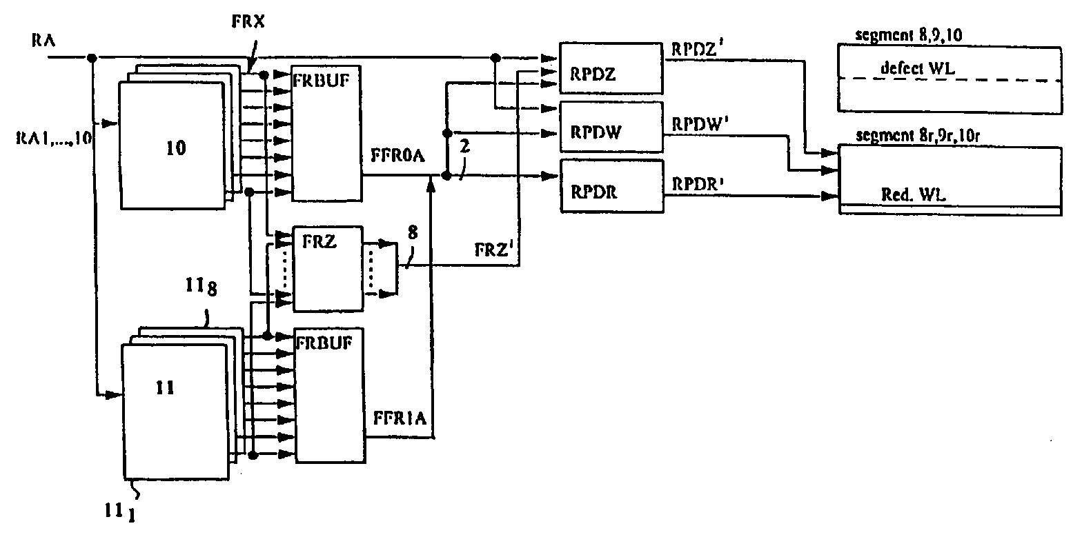
Die Erfindung betrifft eine Redundanzschaltung für Halbleiterspeicher
mit in Segmenten organisierten Wortleitungen
(WL), bei der bei Auftreten einer defekten Wortleitung
(defect WL) in einem Segment (segment 8, 9, 10) mittels den
jeweiligen Segmenten zugeordneten Fuse-Sets (10, 11) durch
Inter-Segment-Redundanz eine redundante Wortleitung (Red. WL)
im gleichen oder in einem anderen Segment durch ein Segmentauswahlsignal
(RPDZ') aktivierbar ist. Das Segmentauswahlsignal
(RPDZ') wird durch Auswertung des Ausgangssignals
der Fuse-Sets direkt erzeugt.
Applications Claiming Priority (2)
| Application Number | Priority Date | Filing Date | Title |
|---|---|---|---|
| DE19729579A DE19729579C2 (en) | 1997-07-10 | 1997-07-10 | Method for activating a redundant word line with inter-segment redundancy in a semiconductor memory with word lines organized in segments |
| DE19729579 | 1997-07-10 |
Publications (2)
| Publication Number | Publication Date |
|---|---|
| EP0890902A2 EP0890902A2 (en) | 1999-01-13 |
| EP0890902A3 true EP0890902A3 (en) | 1999-09-22 |
Family
ID=7835296
Family Applications (1)
| Application Number | Title | Priority Date | Filing Date |
|---|---|---|---|
| EP98112767A Withdrawn EP0890902A3 (en) | 1997-07-10 | 1998-07-09 | Redundancy circuit for semiconductor memory devide |
Country Status (7)
| Country | Link |
|---|---|
| US (1) | US6188617B1 (en) |
| EP (1) | EP0890902A3 (en) |
| JP (1) | JP3660804B2 (en) |
| KR (1) | KR100325649B1 (en) |
| CN (1) | CN1269132C (en) |
| DE (1) | DE19729579C2 (en) |
| TW (1) | TW394955B (en) |
Families Citing this family (3)
| Publication number | Priority date | Publication date | Assignee | Title |
|---|---|---|---|---|
| US6314030B1 (en) * | 2000-06-14 | 2001-11-06 | Micron Technology, Inc. | Semiconductor memory having segmented row repair |
| US7111193B1 (en) * | 2002-07-30 | 2006-09-19 | Taiwan Semiconductor Manufacturing Co. Ltd. | Semiconductor memory having re-configurable fuse set for redundancy repair |
| US7613060B2 (en) | 2007-05-21 | 2009-11-03 | Micron Technology, Inc. | Methods, circuits, and systems to select memory regions |
Citations (2)
| Publication number | Priority date | Publication date | Assignee | Title |
|---|---|---|---|---|
| EP0442319A2 (en) * | 1990-02-14 | 1991-08-21 | Texas Instruments Incorporated | Redundancy scheme for eliminating defects in a memory device |
| EP0554901A2 (en) * | 1992-02-07 | 1993-08-11 | Matsushita Electric Industrial Co., Ltd. | A semiconductor memory device |
Family Cites Families (4)
| Publication number | Priority date | Publication date | Assignee | Title |
|---|---|---|---|---|
| US4754434A (en) * | 1985-08-28 | 1988-06-28 | Advanced Micro Devices, Inc. | Switching plane redundancy |
| DE59205881D1 (en) * | 1992-04-16 | 1996-05-02 | Siemens Ag | INTEGRATED SEMICONDUCTOR MEMORY WITH REDUNDANCY DEVICE |
| KR950004623B1 (en) * | 1992-12-07 | 1995-05-03 | 삼성전자주식회사 | Semiconductor memory device with improved redundancy efficiency |
| KR100192574B1 (en) * | 1995-10-04 | 1999-06-15 | 윤종용 | Column Redundancy Circuit in Semiconductor Memory Devices Using Decoded Fuses |
-
1997
- 1997-07-10 DE DE19729579A patent/DE19729579C2/en not_active Expired - Lifetime
-
1998
- 1998-07-06 TW TW087110889A patent/TW394955B/en not_active IP Right Cessation
- 1998-07-07 JP JP19135398A patent/JP3660804B2/en not_active Expired - Fee Related
- 1998-07-09 EP EP98112767A patent/EP0890902A3/en not_active Withdrawn
- 1998-07-10 CN CNB981159516A patent/CN1269132C/en not_active Expired - Fee Related
- 1998-07-10 KR KR1019980027747A patent/KR100325649B1/en not_active Expired - Fee Related
- 1998-07-13 US US09/115,618 patent/US6188617B1/en not_active Expired - Lifetime
Patent Citations (2)
| Publication number | Priority date | Publication date | Assignee | Title |
|---|---|---|---|---|
| EP0442319A2 (en) * | 1990-02-14 | 1991-08-21 | Texas Instruments Incorporated | Redundancy scheme for eliminating defects in a memory device |
| EP0554901A2 (en) * | 1992-02-07 | 1993-08-11 | Matsushita Electric Industrial Co., Ltd. | A semiconductor memory device |
Also Published As
| Publication number | Publication date |
|---|---|
| EP0890902A2 (en) | 1999-01-13 |
| CN1269132C (en) | 2006-08-09 |
| KR100325649B1 (en) | 2002-05-09 |
| DE19729579C2 (en) | 2000-12-07 |
| JP3660804B2 (en) | 2005-06-15 |
| US6188617B1 (en) | 2001-02-13 |
| KR19990013743A (en) | 1999-02-25 |
| CN1205520A (en) | 1999-01-20 |
| TW394955B (en) | 2000-06-21 |
| DE19729579A1 (en) | 1999-01-14 |
| JPH1173795A (en) | 1999-03-16 |
Similar Documents
| Publication | Publication Date | Title |
|---|---|---|
| DE3483421D1 (en) | DISPERSION-REINFORCED ALUMINUM ALLOY WITH GOOD WEAR AND RESISTANCE AND METHOD FOR THEIR PRODUCTION. | |
| DE19640437B4 (en) | Column redundancy circuit | |
| DE3486076D1 (en) | CORROSION PROTECTED WORKPIECES FROM STEEL AND METHOD FOR THEIR PRODUCTION. | |
| ATE206131T1 (en) | PHOSPHONOMONOESTERNUCLIC ACIDS, METHOD FOR THEIR PRODUCTION AND THEIR USE | |
| DE69731234D1 (en) | METHOD FOR PRODUCING A COMPLETE cDNAS cDNA BANK. | |
| JPH0241118B2 (en) | ||
| EP0929036A3 (en) | Method and apparatus of column redundancy for non-volatile analog and multilevel memory integrated circuits | |
| EP1792980A3 (en) | Collagen biomatrix and methods to poduce it | |
| ATE391994T1 (en) | METHOD FOR RECONFIGURATION OF A MEMORY | |
| DE4441183A1 (en) | Row redundancy circuit for cellular integrated memory, e.g. DRAM with fuseboxes | |
| DE59601917D1 (en) | Wire electrode and method for producing a wire electrode, in particular for the spark erosion method | |
| DE4441007A1 (en) | Multibit testing circuit for semiconductor DRAM | |
| EP1008993A3 (en) | Writeable memory with self-test device and method therefor | |
| EP0849355A3 (en) | Powder washing and cleaning components | |
| EP2298917A3 (en) | Textile-specific promoters | |
| DE68903073D1 (en) | THIN, CORROSION AND HEAT-RESISTANT FILM FROM AN ALUMINUM ALLOY AND METHOD FOR THE PRODUCTION THEREOF. | |
| DE3481120D1 (en) | 3,6-DISUBSTITUTED-1,8-NAPHTHALIMIDES, METHOD FOR THE PRODUCTION THEREOF AND THEIR USE. | |
| WO2004064075A1 (en) | Method for the recognition and/or correction of memory access errors and electronic circuit arrangement for carrying out said method | |
| DE3779478D1 (en) | CONJUGATED (E, Z) -ALKADIA COMPOUNDS SUBSTITUTED IN 1-POSITION AND METHOD FOR THEIR PRODUCTION. | |
| EP0283908A1 (en) | Integrated multistage decoder | |
| DE59507797D1 (en) | SEALING ELEMENT, ESPECIALLY FOR SHUT-OFF AND CONTROL ORGANS AND METHOD FOR THE PRODUCTION THEREOF | |
| DE3578079D1 (en) | AZINE PIGMENTS, METHOD FOR THEIR PRODUCTION AND THEIR USE. | |
| EP0074305A3 (en) | Fault isolating memory decoder | |
| DE19730958B4 (en) | Semiconductor memory device | |
| ATE187826T1 (en) | REDUNDANCY CIRCUIT ARRANGEMENT FOR AN INTEGRATED SEMICONDUCTOR MEMORY |
Legal Events
| Date | Code | Title | Description |
|---|---|---|---|
| PUAI | Public reference made under article 153(3) epc to a published international application that has entered the european phase |
Free format text: ORIGINAL CODE: 0009012 |
|
| AK | Designated contracting states |
Kind code of ref document: A2 Designated state(s): DE FR GB IE IT NL |
|
| AX | Request for extension of the european patent |
Free format text: AL;LT;LV;MK;RO;SI |
|
| PUAL | Search report despatched |
Free format text: ORIGINAL CODE: 0009013 |
|
| AK | Designated contracting states |
Kind code of ref document: A3 Designated state(s): AT BE CH CY DE DK ES FI FR GB GR IE IT LI LU MC NL PT SE |
|
| AX | Request for extension of the european patent |
Free format text: AL;LT;LV;MK;RO;SI |
|
| 17P | Request for examination filed |
Effective date: 20000121 |
|
| AKX | Designation fees paid |
Free format text: DE FR GB IE IT NL |
|
| RAP1 | Party data changed (applicant data changed or rights of an application transferred) |
Owner name: INFINEON TECHNOLOGIES AG |
|
| 17Q | First examination report despatched |
Effective date: 20010928 |
|
| STAA | Information on the status of an ep patent application or granted ep patent |
Free format text: STATUS: THE APPLICATION IS DEEMED TO BE WITHDRAWN |
|
| 18D | Application deemed to be withdrawn |
Effective date: 20020309 |