EP0890945A1 - Procédé d'enregistrement par exposition de matériaux optiques d'enregistrement - Google Patents
Procédé d'enregistrement par exposition de matériaux optiques d'enregistrement Download PDFInfo
- Publication number
- EP0890945A1 EP0890945A1 EP98112586A EP98112586A EP0890945A1 EP 0890945 A1 EP0890945 A1 EP 0890945A1 EP 98112586 A EP98112586 A EP 98112586A EP 98112586 A EP98112586 A EP 98112586A EP 0890945 A1 EP0890945 A1 EP 0890945A1
- Authority
- EP
- European Patent Office
- Prior art keywords
- exposure
- light beam
- recording method
- photoresist
- objective lens
- Prior art date
- Legal status (The legal status is an assumption and is not a legal conclusion. Google has not performed a legal analysis and makes no representation as to the accuracy of the status listed.)
- Granted
Links
Images

Classifications
-
- G—PHYSICS
- G11—INFORMATION STORAGE
- G11B—INFORMATION STORAGE BASED ON RELATIVE MOVEMENT BETWEEN RECORD CARRIER AND TRANSDUCER
- G11B7/00—Recording or reproducing by optical means, e.g. recording using a thermal beam of optical radiation by modifying optical properties or the physical structure, reproducing using an optical beam at lower power by sensing optical properties; Record carriers therefor
- G11B7/24—Record carriers characterised by shape, structure or physical properties, or by the selection of the material
- G11B7/26—Apparatus or processes specially adapted for the manufacture of record carriers
- G11B7/261—Preparing a master, e.g. exposing photoresist, electroforming
-
- Y—GENERAL TAGGING OF NEW TECHNOLOGICAL DEVELOPMENTS; GENERAL TAGGING OF CROSS-SECTIONAL TECHNOLOGIES SPANNING OVER SEVERAL SECTIONS OF THE IPC; TECHNICAL SUBJECTS COVERED BY FORMER USPC CROSS-REFERENCE ART COLLECTIONS [XRACs] AND DIGESTS
- Y10—TECHNICAL SUBJECTS COVERED BY FORMER USPC
- Y10S—TECHNICAL SUBJECTS COVERED BY FORMER USPC CROSS-REFERENCE ART COLLECTIONS [XRACs] AND DIGESTS
- Y10S430/00—Radiation imagery chemistry: process, composition, or product thereof
- Y10S430/146—Laser beam
Definitions
- the present invention relates to an exposure recording method for optical recording materials, and more particularly to an exposure recording method for optical recording materials which is characterized by a photoresist-film exposure recording method using light beams.
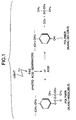
- Fig. 1 shows a polymer in which a hydroxyl group of polyvinyl phenol is protected by a tert-butoxycarbonyl group and a photochemical reaction process of a chemically amplified photoresist formed of a photo acid generator (PAG).
- PAG photo acid generator
- the chemically amplified photoresist is formed of the polymer and the photo acid generator.
- the photo acid generator is exposed to light to generate acid, the acid thus generated is thermally diffused by a heat treatment to induce reaction of the polymer, and solubility to developing liquid is varied to form a pattern.
- the acid which is generated in the exposure process reforms the alkali-insoluble polymer into alkali-soluble material under a heating condition. That is, the exposed portion serves as a positive type resist which is removed in a developing process. Accordingly, when the chemically amplified photoresist is used, the heat treatment process after the exposure process is indispensable, and many steps in connection with the heat treatment are needed.
- the sensitivity of the chemically amplified photoresists is generally instable and it is more difficult to handle these photoresists than the novolak photoresists.
- One of causes resides in that the diffusion of the acid generated in the exposure process is suppressed by ammonium, etc. in the air before the heat treatment process is carried out. It is needless to say that the degree of the inactivation is dependent on the time period from the exposure process until the heat treatment process.
- the present invention has an object to provide an exposure recording method which can enhance productivity in a heat treatment process after an exposure process of a photoresist in the photolithography process in a far ultraviolet radiation region, and stabilize the characteristic of the photoresist after the exposure process.
- an exposure recording method for optical recording materials which comprises an exposure step for exposing a chemical amplification type photoresist or other types of photoresist to a light beam which is focused by an objective lens, and a heat treatment step for performing a heat treatment to reform an exposed portion of the photoresist after the exposure process, is characterized in that the power density of the light beam is set to 4 ⁇ x 10 2 W/cm 2 ( ⁇ [cm/sec] represents a linear velocity of recording) or more, and the exposure process and the heat treatment process are simultaneously carried out.
- the numeral aperture NA of the objective lens is set to 0.85 or more
- the light source for emitting the light beam comprises an excimer laser for emitting light having a wavelength of 300nm or less, or an all solid state laser for achieving forth harmonic generation of YAG laser by using a nonlinear optical crystal.
- the chemically amplified photoresist or the like is exposed to the light beam which is converged until a diffraction limit level by using an objective lens having a large numerical aperture and has a large power density, whereby the exposure process and the heat treatment process can be simultaneously carried out, whereby the heat treatment process after the exposure process is unnecessary.
- the patterning characteristic which is dependent on the time different from the exposure process to the heat treatment process is made excellent.
- Fig. 2 is a diagram showing an exposure recording device for a master disc of an optical disc which uses a far ultraviolet radiation laser as a light source.
- a light source laser 1 As a light source laser 1 is used an all solid state laser for performing forth harmonic generation of YAG laser by using non-linear optical crystal.
- the numerical aperture of an objective lens 7 is set to 0.85 or more.
- a laser beam emitted from the light source laser 1 is transmitted through a power controller 2 comprising an electrooptical element, a polarizing beam splitter, a photodetector, etc., reflected by a first mirror 3a while the optical path thereof is bent by 90 degrees, and then enters a light modulator 5.
- the laser beam is modulated with a signal which is supplied from a signal generator 4, and then reflected by a second mirror 3b while the optical path thereof is bent by 90 degrees.
- the laser beam is expanded by a beam expander comprising two or more lens 6 so that the spot diameter of the laser beam is equal to or larger than the entrance pupil diameter, reflected by a third mirror 3c so that the optical path thereof is bent by 90 degrees, enters the objective lens 7, and then irradiated onto the photoresist 8 at a large power density.
- the objective lens 7 whose numerical aperture is set to 0.85 or more is designed to be movable integrally with the third mirror 3c in a radial direction of the master disc 9 of the optical disc which is coated with the photoresist 8.
- the objective lens 7 is moved at a constant velocity while the master disc 9 of the optical disc is rotated on a turn table 10, thereby performing a spiral exposure recording operation.
- the exposure area per unit time is calculated into (4 x 10 -5 cm) x ⁇ cm/sec, where ⁇ [cm/sec] represents a linear velocity of recording.
- the power of recording far ultraviolet radiation after emitted from the objective lens 7 which achieves the light energy density of about 10 -2 J/cm 2 which is generally needed when the exposure recording is carried out on the chemically amplified photoresist 8 with far ultraviolet radiation, is calculated into (10 -2 J/cm 2 ) x (4 ⁇ x 10 -5 cm 2 /sec), and thus 4v x 10 -7 W.
- the power density of the recording far ultraviolet radiation is equal to 4 ⁇ x 10 -7 [W] / 10 -9 cm 2 , and thus 4 ⁇ x 10 2 [W/cm 2 ].
- ⁇ is set to 10 2 to 10 3 cm/sec, and thus the power density is equal to 4 x 10 4 to 4 x 10 5 [W/cm 2 ].
- This value shows that the recording operation of the master disc of the optical disc needs very large power density unlike such a case that a stationary photoresist 8 is exposed to light, for example, in the case of a photolithography of semiconductor devices in which the recording power density is equal to about 10 -1 [W/cm 2 ].
- a light beam of 300nm or less in wavelength is used and the numerical aperture of the objective lens 7 is set to 0.85 or more, whereby the power density of a spot portion focused onto the photoresist 8 can be set to 1 x 10 4 [W/cm 2 ] or more.
- the photoresist 8 can be instantaneously heated to several tens to one hundred and several tens °C.
- the power density of the light beam was equal to about 3.6 x 10 -5 cm because the spot diameter of the light beam can be expressed by the relational expression: 1.22 x (wavelength/numerical aperture). Further, since the area of the light beam was equal to about 1 x 10 -9 cm 2 , (the recording power 3 x 10 -4 W)/(light beam spot area 1 x 10 -9 cm 2 ) is equal to about 3 x 10 5 W/cm 2 .
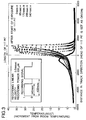
- This calculation is applied to a case where the exposure recording is newly carried out on a pit when a pit of 340 nsec (exposed portion) and a land of 93 nsec (non-exposed portion) are repeated.
- Fig. 3 shows a simulation result of the temperature distribution in the track direction in the pulse exposure recording operation.
- the temperature of the exposed portion of the photoresist 8 rises up to about 60°C at maximum.
- the minimum value of the heat treatment temperature after the exposure process is equal to about 50°C, so that if the temperature of the exposed portion of the photoresist rises up to 60°C or more, this operation can sufficiently play the same role as the heat treatment process after the exposure process.
Landscapes
- Engineering & Computer Science (AREA)
- Manufacturing & Machinery (AREA)
- Exposure And Positioning Against Photoresist Photosensitive Materials (AREA)
- Manufacturing Optical Record Carriers (AREA)
- Photosensitive Polymer And Photoresist Processing (AREA)
- Materials For Photolithography (AREA)
- Optical Head (AREA)
- Exposure Of Semiconductors, Excluding Electron Or Ion Beam Exposure (AREA)
Applications Claiming Priority (3)
| Application Number | Priority Date | Filing Date | Title |
|---|---|---|---|
| JP18670697 | 1997-07-11 | ||
| JP186706/97 | 1997-07-11 | ||
| JP9186706A JPH1139728A (ja) | 1997-07-11 | 1997-07-11 | 光記録材料の露光記録方法 |
Publications (2)
| Publication Number | Publication Date |
|---|---|
| EP0890945A1 true EP0890945A1 (fr) | 1999-01-13 |
| EP0890945B1 EP0890945B1 (fr) | 2001-11-21 |
Family
ID=16193219
Family Applications (1)
| Application Number | Title | Priority Date | Filing Date |
|---|---|---|---|
| EP98112586A Expired - Lifetime EP0890945B1 (fr) | 1997-07-11 | 1998-07-07 | Procédé d'enregistrement par exposition de matériaux optiques d'enregistrement |
Country Status (8)
| Country | Link |
|---|---|
| US (1) | US6048669A (fr) |
| EP (1) | EP0890945B1 (fr) |
| JP (1) | JPH1139728A (fr) |
| KR (1) | KR100525342B1 (fr) |
| DE (1) | DE69803246T2 (fr) |
| MY (1) | MY121320A (fr) |
| SG (1) | SG67519A1 (fr) |
| TW (1) | TW374896B (fr) |
Families Citing this family (2)
| Publication number | Priority date | Publication date | Assignee | Title |
|---|---|---|---|---|
| JP2004005872A (ja) * | 2002-04-09 | 2004-01-08 | Matsushita Electric Ind Co Ltd | 光ディスク原盤作製方法および光ディスクとその製造方法 |
| US8617784B2 (en) * | 2006-05-26 | 2013-12-31 | Intel Corporation | Increasing photoresist processing throughput |
Citations (2)
| Publication number | Priority date | Publication date | Assignee | Title |
|---|---|---|---|---|
| JPH0447542A (ja) * | 1990-06-15 | 1992-02-17 | Mitsubishi Electric Corp | 光ディスク原盤の製造方法 |
| EP0596439A2 (fr) * | 1992-11-05 | 1994-05-11 | Matsushita Electric Industrial Co., Ltd. | Procédé de fabrication d'un disque-mère utilisable pour la production de disques optiques |
Family Cites Families (11)
| Publication number | Priority date | Publication date | Assignee | Title |
|---|---|---|---|---|
| GB8629223D0 (en) * | 1986-12-06 | 1987-01-14 | Emi Plc Thorn | Replication of carriers |
| CA1303740C (fr) * | 1987-08-21 | 1992-06-16 | Kazuo Van | Disque optique pour memoires optiques |
| US5191565A (en) * | 1989-06-19 | 1993-03-02 | Matsushita Electric Industrial Co., Ltd. | Optical information recording medium |
| JPH0447535A (ja) * | 1990-06-15 | 1992-02-17 | Pioneer Electron Corp | 光学的記録方法 |
| JP3006199B2 (ja) * | 1991-09-03 | 2000-02-07 | 株式会社日立製作所 | 光ディスクの製造方法 |
| US5384758A (en) * | 1991-12-02 | 1995-01-24 | Nikon Corporation | Reproduction-only magneto-optical disk with selectively exchange coupled layers, and reproduction method and reproduction apparatus therefor |
| US5559338A (en) * | 1994-10-04 | 1996-09-24 | Excimer Laser Systems, Inc. | Deep ultraviolet optical imaging system for microlithography and/or microfabrication |
| EP0709410A3 (fr) * | 1994-10-26 | 1997-03-26 | Ocg Microelectronic Materials | Polymères |
| JPH08313805A (ja) * | 1995-05-18 | 1996-11-29 | Sony Corp | レンズ装置及び紫外線集光装置 |
| US5652645A (en) * | 1995-07-24 | 1997-07-29 | Anvik Corporation | High-throughput, high-resolution, projection patterning system for large, flexible, roll-fed, electronic-module substrates |
| JPH0950951A (ja) * | 1995-08-04 | 1997-02-18 | Nikon Corp | リソグラフィ方法およびリソグラフィ装置 |
-
1997
- 1997-07-11 JP JP9186706A patent/JPH1139728A/ja active Pending
-
1998
- 1998-07-02 TW TW087110721A patent/TW374896B/zh not_active IP Right Cessation
- 1998-07-04 SG SG1998001590A patent/SG67519A1/en unknown
- 1998-07-07 EP EP98112586A patent/EP0890945B1/fr not_active Expired - Lifetime
- 1998-07-07 DE DE69803246T patent/DE69803246T2/de not_active Expired - Fee Related
- 1998-07-09 MY MYPI98003129A patent/MY121320A/en unknown
- 1998-07-10 KR KR10-1998-0027860A patent/KR100525342B1/ko not_active Expired - Fee Related
- 1998-07-10 US US09/112,946 patent/US6048669A/en not_active Expired - Fee Related
Patent Citations (2)
| Publication number | Priority date | Publication date | Assignee | Title |
|---|---|---|---|---|
| JPH0447542A (ja) * | 1990-06-15 | 1992-02-17 | Mitsubishi Electric Corp | 光ディスク原盤の製造方法 |
| EP0596439A2 (fr) * | 1992-11-05 | 1994-05-11 | Matsushita Electric Industrial Co., Ltd. | Procédé de fabrication d'un disque-mère utilisable pour la production de disques optiques |
Non-Patent Citations (2)
| Title |
|---|
| MCMURDIE N D, O'DWYER J B: "Advances in Resist Technology and Processing XIII, Santa Clara, CA, USA, 11-13 March 1996", PROC. SPIE - INT. SOC. OPT. ENG. (USA), PROCEEDINGS OF THE SPIE - THE INTERNATIONAL SOCIETY FOR OPTICAL ENGINEERING, 1996, SPIE - INT. SOC. OPT. ENG., USA, XP002079214 * |
| PATENT ABSTRACTS OF JAPAN vol. 016, no. 225 (P - 1360) 26 May 1992 (1992-05-26) * |
Also Published As
| Publication number | Publication date |
|---|---|
| DE69803246D1 (de) | 2002-02-21 |
| KR19990013773A (ko) | 1999-02-25 |
| MY121320A (en) | 2006-01-28 |
| DE69803246T2 (de) | 2002-08-22 |
| EP0890945B1 (fr) | 2001-11-21 |
| US6048669A (en) | 2000-04-11 |
| SG67519A1 (en) | 1999-09-21 |
| JPH1139728A (ja) | 1999-02-12 |
| KR100525342B1 (ko) | 2005-12-28 |
| TW374896B (en) | 1999-11-21 |
Similar Documents
| Publication | Publication Date | Title |
|---|---|---|
| JP4329208B2 (ja) | 記録媒体の製造方法、記録媒体製造用原盤の製造方法、記録媒体の製造装置、および記録媒体製造用原盤の製造装置 | |
| US6048669A (en) | Exposure recording method for optical recording materials | |
| GB2368652A (en) | Resist exposure system with heating apparatus | |
| JPH04241237A (ja) | 高密度記録ディスク用スタンパとその製造方法 | |
| US6100012A (en) | Infra-red radiation post-exposure bake process for chemically amplified resist lithography | |
| JP2001250280A (ja) | 記録媒体、記録媒体の製造方法、記録媒体製造用原盤の製造方法、記録媒体の製造装置、および記録媒体製造用原盤の製造装置 | |
| EP0596439A2 (fr) | Procédé de fabrication d'un disque-mère utilisable pour la production de disques optiques | |
| US5215869A (en) | Process of forming a permanent yellow imaged light modulating film | |
| JP2001243663A (ja) | 記録媒体の製造方法、記録媒体製造用原盤の製造方法、記録媒体の製造装置、および記録媒体製造用原盤の製造装置 | |
| JP2585861B2 (ja) | 光メモリ素子用フォトマスクの製造方法 | |
| Mejiritski et al. | Novel Photoimaging System Based on Photoinduced Electron Transfer in Polymers Containing Pendant Benzophenone− Borate Salts | |
| EP0111655A1 (fr) | Procédé pour la fabrication de dessins autodéveloppants utilisant une photoréserve positive | |
| EP1492093A1 (fr) | Procede de traitement pour une matrice en resine photosensible, procede de production d'une matrice utilisant un support d'enregistrement, procede de production d'un support d'enregistrement, matrice en resine photosensible, matrice utilisant un support d'enregistrment et support d'enregistrem | |
| JPH07106234A (ja) | レジストパターンの形成方法 | |
| EP0595361B1 (fr) | Procédé de réalisation de micro-images résistantes à la chaleur | |
| US5139926A (en) | Permanent yellow imaged light modulating film | |
| JP2001243664A (ja) | 記録媒体の製造方法、記録媒体製造用原盤の製造方法、記録媒体の製造装置、および記録媒体製造用原盤の製造装置 | |
| KR100674932B1 (ko) | Pag및 tag를 포함하는 화학증폭형 포토레지스트 조성물을 이용한 반도체 소자의 미세 패턴 형성 방법 | |
| JP4219773B2 (ja) | 光反応解析装置 | |
| JPH04342260A (ja) | レジストパターンの形成方法 | |
| KR100278915B1 (ko) | 반도체 소자의 감광막 패턴 제조방법 | |
| JP4687782B2 (ja) | 記録媒体の製造方法、および記録媒体製造用原盤の製造方法 | |
| JPH06266105A (ja) | ネガ型レジスト組成物 | |
| JP2004281874A (ja) | レジストパターン形成方法およびレジストパターン形成システム | |
| JP2511102B2 (ja) | 光ディスクの製造方法 |
Legal Events
| Date | Code | Title | Description |
|---|---|---|---|
| PUAI | Public reference made under article 153(3) epc to a published international application that has entered the european phase |
Free format text: ORIGINAL CODE: 0009012 |
|
| AK | Designated contracting states |
Kind code of ref document: A1 Designated state(s): DE FR GB |
|
| AX | Request for extension of the european patent |
Free format text: AL;LT;LV;MK;RO;SI |
|
| 17P | Request for examination filed |
Effective date: 19990615 |
|
| AKX | Designation fees paid |
Free format text: DE FR GB |
|
| 17Q | First examination report despatched |
Effective date: 20000225 |
|
| GRAG | Despatch of communication of intention to grant |
Free format text: ORIGINAL CODE: EPIDOS AGRA |
|
| GRAG | Despatch of communication of intention to grant |
Free format text: ORIGINAL CODE: EPIDOS AGRA |
|
| GRAG | Despatch of communication of intention to grant |
Free format text: ORIGINAL CODE: EPIDOS AGRA |
|
| GRAH | Despatch of communication of intention to grant a patent |
Free format text: ORIGINAL CODE: EPIDOS IGRA |
|
| GRAH | Despatch of communication of intention to grant a patent |
Free format text: ORIGINAL CODE: EPIDOS IGRA |
|
| GRAA | (expected) grant |
Free format text: ORIGINAL CODE: 0009210 |
|
| AK | Designated contracting states |
Kind code of ref document: B1 Designated state(s): DE FR GB |
|
| REG | Reference to a national code |
Ref country code: GB Ref legal event code: IF02 |
|
| REF | Corresponds to: |
Ref document number: 69803246 Country of ref document: DE Date of ref document: 20020221 |
|
| ET | Fr: translation filed | ||
| PLBE | No opposition filed within time limit |
Free format text: ORIGINAL CODE: 0009261 |
|
| STAA | Information on the status of an ep patent application or granted ep patent |
Free format text: STATUS: NO OPPOSITION FILED WITHIN TIME LIMIT |
|
| 26N | No opposition filed | ||
| PGFP | Annual fee paid to national office [announced via postgrant information from national office to epo] |
Ref country code: DE Payment date: 20080711 Year of fee payment: 11 |
|
| PGFP | Annual fee paid to national office [announced via postgrant information from national office to epo] |
Ref country code: FR Payment date: 20080718 Year of fee payment: 11 |
|
| PGFP | Annual fee paid to national office [announced via postgrant information from national office to epo] |
Ref country code: GB Payment date: 20080709 Year of fee payment: 11 |
|
| GBPC | Gb: european patent ceased through non-payment of renewal fee |
Effective date: 20090707 |
|
| REG | Reference to a national code |
Ref country code: FR Ref legal event code: ST Effective date: 20100331 |
|
| PG25 | Lapsed in a contracting state [announced via postgrant information from national office to epo] |
Ref country code: FR Free format text: LAPSE BECAUSE OF NON-PAYMENT OF DUE FEES Effective date: 20090731 |
|
| PG25 | Lapsed in a contracting state [announced via postgrant information from national office to epo] |
Ref country code: GB Free format text: LAPSE BECAUSE OF NON-PAYMENT OF DUE FEES Effective date: 20090707 |
|
| PG25 | Lapsed in a contracting state [announced via postgrant information from national office to epo] |
Ref country code: DE Free format text: LAPSE BECAUSE OF NON-PAYMENT OF DUE FEES Effective date: 20100202 |