EP0891122A1 - Organische elektrolumineszente Vorrichtung - Google Patents
Organische elektrolumineszente Vorrichtung Download PDFInfo
- Publication number
- EP0891122A1 EP0891122A1 EP98305445A EP98305445A EP0891122A1 EP 0891122 A1 EP0891122 A1 EP 0891122A1 EP 98305445 A EP98305445 A EP 98305445A EP 98305445 A EP98305445 A EP 98305445A EP 0891122 A1 EP0891122 A1 EP 0891122A1
- Authority
- EP
- European Patent Office
- Prior art keywords
- electrode
- organic
- layer
- transparent electrode
- aluminum
- Prior art date
- Legal status (The legal status is an assumption and is not a legal conclusion. Google has not performed a legal analysis and makes no representation as to the accuracy of the status listed.)
- Withdrawn
Links
Images




Classifications
-
- H—ELECTRICITY
- H05—ELECTRIC TECHNIQUES NOT OTHERWISE PROVIDED FOR
- H05B—ELECTRIC HEATING; ELECTRIC LIGHT SOURCES NOT OTHERWISE PROVIDED FOR; CIRCUIT ARRANGEMENTS FOR ELECTRIC LIGHT SOURCES, IN GENERAL
- H05B33/00—Electroluminescent light sources
- H05B33/12—Light sources with substantially two-dimensional [2D] radiating surfaces
- H05B33/26—Light sources with substantially two-dimensional [2D] radiating surfaces characterised by the composition or arrangement of the conductive material used as an electrode
- H05B33/28—Light sources with substantially two-dimensional [2D] radiating surfaces characterised by the composition or arrangement of the conductive material used as an electrode of translucent electrodes
-
- H—ELECTRICITY
- H05—ELECTRIC TECHNIQUES NOT OTHERWISE PROVIDED FOR
- H05B—ELECTRIC HEATING; ELECTRIC LIGHT SOURCES NOT OTHERWISE PROVIDED FOR; CIRCUIT ARRANGEMENTS FOR ELECTRIC LIGHT SOURCES, IN GENERAL
- H05B33/00—Electroluminescent light sources
- H05B33/12—Light sources with substantially two-dimensional [2D] radiating surfaces
- H05B33/26—Light sources with substantially two-dimensional [2D] radiating surfaces characterised by the composition or arrangement of the conductive material used as an electrode
-
- H—ELECTRICITY
- H10—SEMICONDUCTOR DEVICES; ELECTRIC SOLID-STATE DEVICES NOT OTHERWISE PROVIDED FOR
- H10K—ORGANIC ELECTRIC SOLID-STATE DEVICES
- H10K50/00—Organic light-emitting devices
- H10K50/80—Constructional details
- H10K50/805—Electrodes
- H10K50/81—Anodes
- H10K50/814—Anodes combined with auxiliary electrodes, e.g. ITO layer combined with metal lines
-
- H—ELECTRICITY
- H10—SEMICONDUCTOR DEVICES; ELECTRIC SOLID-STATE DEVICES NOT OTHERWISE PROVIDED FOR
- H10K—ORGANIC ELECTRIC SOLID-STATE DEVICES
- H10K59/00—Integrated devices, or assemblies of multiple devices, comprising at least one organic light-emitting element covered by group H10K50/00
- H10K59/10—OLED displays
- H10K59/17—Passive-matrix OLED displays
- H10K59/179—Interconnections, e.g. wiring lines or terminals
- H10K59/1795—Interconnections, e.g. wiring lines or terminals comprising structures specially adapted for lowering the resistance
-
- H—ELECTRICITY
- H10—SEMICONDUCTOR DEVICES; ELECTRIC SOLID-STATE DEVICES NOT OTHERWISE PROVIDED FOR
- H10K—ORGANIC ELECTRIC SOLID-STATE DEVICES
- H10K59/00—Integrated devices, or assemblies of multiple devices, comprising at least one organic light-emitting element covered by group H10K50/00
- H10K59/80—Constructional details
- H10K59/805—Electrodes
- H10K59/8051—Anodes
- H10K59/80516—Anodes combined with auxiliary electrodes, e.g. ITO layer combined with metal lines
-
- H—ELECTRICITY
- H10—SEMICONDUCTOR DEVICES; ELECTRIC SOLID-STATE DEVICES NOT OTHERWISE PROVIDED FOR
- H10K—ORGANIC ELECTRIC SOLID-STATE DEVICES
- H10K59/00—Integrated devices, or assemblies of multiple devices, comprising at least one organic light-emitting element covered by group H10K50/00
- H10K59/10—OLED displays
-
- H—ELECTRICITY
- H10—SEMICONDUCTOR DEVICES; ELECTRIC SOLID-STATE DEVICES NOT OTHERWISE PROVIDED FOR
- H10K—ORGANIC ELECTRIC SOLID-STATE DEVICES
- H10K59/00—Integrated devices, or assemblies of multiple devices, comprising at least one organic light-emitting element covered by group H10K50/00
- H10K59/10—OLED displays
- H10K59/19—Segment displays
Definitions
- the present invention relates generally to an organic EL (electroluminescent) device, and specifically to an improvement in or relating to a hole injecting electrode for feeding holes (charges) to a light emitting layer.
- organic EL devices have been under intensive investigation.
- One such device is basically built up of a thin film form of hole transporting material such as triphenyldiamine (TPD) deposited by evaporation on a hole injecting electrode, a light emitting layer of fluorescent material such as an aluminum quinolinol complex (Alq 3 ) laminated thereon, and a metal (electron injecting) electrode of a metal having a low work function such as Mg and formed on the light emitting layer.
- TPD triphenyldiamine
- Alq 3 aluminum quinolinol complex
- Mg metal having a low work function
- a hole injecting electrode considered to be effective for such organic EL devices is made up of a material capable of injecting more electrons into a light emitting layer or a hole injecting and transporting layer.
- One requirement for the material is that it be transparent and electrically conductive because, in most cases, an organic EL device is usually designed to take out the emitted light from a substrate side thereof.
- ITO in-doped indium oxide
- IZO zinc-doped indium oxide
- ZnO zinc-doped indium oxide
- SnO 2 In 2 O 3 , etc.
- ITO electrodes have a visible light transmittance of 90% or higher and a sheet resistance of 10 ⁇ / ⁇ or lower, and so find wide applications as transparent electrodes for liquid crystal displays (LCDs), dimmer glasses, and solar batteries.
- the ITO electrodes are also considered to be promising for hole injecting electrodes in the organic EL devices.
- An organic EL device requires a given current for light emission, and the light emission luminance increases in proportion to an applied current density. Consequently, when sophisticated display patterns or large-screen displays are driven with high luminance or at a high duty ratio, the resistance of interconnecting lines in the hole injecting electrode is found to give rise to a voltage drop problem, although this resistance is negligible when the length of interconnecting lines is short. If, for example, a display of 256 dots x 64 dots is driven at a light emission luminance of 150 cd/m 2 , a 1/64 second-light emission will occur at a light emission luminance of 150 x 64 cd/m 2 .
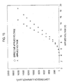
- the device When the sheet resistance of the hole injecting electrode is sufficiently reduced, the device may be driven at a voltage value approximate to an effective applied voltage shown in Fig. 15 for instance.
- the resistance of the hole injecting electrode is about 260 ⁇ , however, a voltage increase of as high as 2 V is needed, as can be seen from the applied voltage shown in Fig. 15.
- Embodiments of the invention seek to provide an organic EL device which can lower the interconnecting resistance of a hole injecting electrode, and so easily accommodate itself to a sophisticated display pattern or large-screen display designed to be driven with high luminance or at a high duty ratio.
- Figure 1 is a general representation illustrative of a 7-segment type hole injecting electrode that is a first embodiment of the organic EL device according to the invention.
- Figure 2 is a sectional view of Fig. 1 as taken along the A-A' line.
- Figure 3 is a general representation illustrative of the process of forming a simple matrix type hole injecting electrode that is a second embodiment of the organic EL device according to the invention.
- Figure 4 is a sectional view of Fig. 3 as taken along the B-B' line.
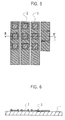
- Figure 5 is a general representation illustrative of the second embodiment of the organic EL device according to the invention, in which the process of forming the metal electrode is illustrated.
- Figure 6 is a sectional view of Fig. 5 as taken along the B-B' line.
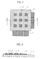
- Figure 7 is a general representation illustrative of the second embodiment of the organic EL device according to the invention, in which the process of forming the insulating film is illustrated.
- Figure 8 is a sectional view of Fig. 7 as taken along the B-B' line.
- Figure 9 is a general representation illustrative of the second embodiment of the organic EL device according to the invention, in which the process of forming the element-isolating structure is illustrated.
- Figure 10 is a sectional view of Fig. 9 as taken along the C-C' line.
- Figure 11 is a general representation illustrative of the second embodiment of the organic EL device according to the invention, in which the process of mask lamination is illustrated.
- Figure 12 is a sectional view of Fig. 11 as taken along the C-C' line.
- Figure 13 is a partial plan view illustrative of one exemplary pattern of the ITO transparent electrode and metal electrode according to the invention.
- Figure 14 is a sectional view of Fig. 13 as taken along the D-D' line.
- Figure 15 is a graph illustrative of a specific applied voltage vs. light emission luminance relation of the organic EL device.
- the organic EL device of the invention comprises a hole injecting electrode, an electron injecting electrode, and at least one organic layer interleaved between both the electrodes.
- the hole injecting electrode comprises a transparent electrode at a light emitting area, and a metal electrode located at a portion other than the light emitting area and electrically connected to the transparent electrode, and having a sheet resistance of 1 ⁇ / ⁇ or lower.
- the transparent electrode is located at the light emitting area out of which light should be taken, and the metal electrode having a low sheet resistance is located at the non-light emitting area out of which light may not be taken, so that the overall resistance value of the hole injecting electrode can remain low.
- the metal electrode is connected to all the peripheral or circumferential area of the transparent electrode.
- the transparent electrode is located at least at the light emitting area (pixel area).
- light emitting area used herein is intended by an area at which a light emitting layer can give out light, and out of which the emitted light can be taken for use. While the transparent electrode area may be larger than the light emitting area, for instance, the transparent electrode may extend slightly from the periphery of the light emitting area, it is to be understood that as the transparent electrode area becomes larger than required, the resistance of the hole injecting electrode becomes high. Thus, it is preferred that the transparent electrode area is equal to, or slightly larger than, the light emitting area.
- ITO in-doped indium oxide
- IZO zinc-doped indium oxide
- ZnO zinc-doped indium oxide
- SnO 2 titanium oxide
- IZO zinc-doped indium oxide
- ZnO zinc-doped indium oxide
- ITO, and IZO may contain an oxide form of Sn, Ti, Pb, etc. in an amount of up to 1 wt% calculated as oxide.
- the transparent electrode may have at least a certain thickness enough to inject holes, and is usually in the range of 10 to 100 nm. However, a thickness of 30 to 100 nm, and especially 50 to 90 nm is preferred. At a film thickness of up to 100 nm, the transparent electrode has so low surface roughness that its surface properties can be improved, resulting in improvements in light emission properties, light emission life, etc. Too large a thickness offers problems in conjunction with film thickness upon film formation, and the ability of the electrode to transport holes.
- the metal electrode has a sheet resistance of preferably 1 ⁇ / ⁇ or lower, and especially 0.5 ⁇ / ⁇ or lower. Although there is no lower limit on sheet resistance, a sheet resistance of about 0.1 ⁇ / ⁇ is generally preferred.
- the metal electrode has a thickness of the order of preferably 10 to 2,000 nm, especially 20 to 1,000 nm, and more especially 100 to 500 nm.
- the metal electrode may be made up of metals such as Al, Cu, Au and Ag, or alloys of Al with transition elements such as Sc, Nb, Zr, Hf, Nd, Ta, Cu, Si, Cr, Mo, Mn, Ni, Pd, Pt, and W.
- metals such as Al, Cu, Au and Ag
- alloys of Al with transition elements such as Sc, Nb, Zr, Hf, Nd, Ta, Cu, Si, Cr, Mo, Mn, Ni, Pd, Pt, and W.
- transition elements such as Sc, Nb, Zr, Hf, Nd, Ta, Cu, Si, Cr, Mo, Mn, Ni, Pd, Pt, and W.
- transition elements such as Sc, Nb, Zr, Hf, Nd, Ta, Cu, Si, Cr, Mo, Mn, Ni, Pd, Pt, and W.
- Al and Al alloys, among which an alloy of Al with at least one transition element is most preferred with an Al content of 90 at% or higher, and
- a barrier metal layer is provided between the transparent electrode and the metal electrode.
- the barrier metal layer may be made up of metals such as Cr and Ti, and nitrides such as titanium nitride (TiN).
- TiN titanium nitride
- particular preference is given to Cr, and TiN, because they can be wet etched with a specific reagent having no attack on the transparent electrode such as an ITO electrode.
- the barrier metal layer has a thickness of 10 to 200 nm, and especially 30 to 100 nm.
- the transparent electrode, metal electrode, and barrier metal layer may be formed as by evaporation, but should preferably be formed by a sputtering technique.
- a sputtering process is applied to the formation of an ITO or IZO transparent electrode, it is preferable to use a target comprising In 2 O 3 doped with SnO 2 or ZnO.
- the metal electrode or barrier electrode in a film form it is preferable to form a sintered product of the aforesaid starting metal material or its alloy by means of a DC or RF sputtering process.
- An ITO transparent electrode when formed by the sputtering technique, suffers a lesser light emission luminance change as compared with an electrode formed by evaporation.
- Power input is preferably in the range of 0.1 to 4 W/cm 2 .
- Power input for a DC sputtering system in particular is preferably in the range of 0.1 to 10 W/cm 2, and especially 0.2 to 5 W/cm 2 .
- the film forming rate is preferably in the range of 2 to 100 nm/min., and especially 5 to 50 nm/min.
- an inert gas such as Ar, He, Ne, Kr, and Xe or a mixture of such inert gases is used as the sputtering gas.
- the sputtering pressure of such gases may usually be of the order of 0.1 to 20 Pa.
- etching solution used for wet etching is preferably an aqueous system for an ITO transparent electrode, and a mixed solution system of phosphoric acid, nitric acid and acetic acid is preferable for a specific metal electrode, e.g., an Al electrode. In the latter case, it is preferable to use an etching solution that enables a specific metal to be selectively etched.
- Fig. 1 is a general representation of one embodiment of the hole injecting electrode according to the invention
- Fig. 2 is a sectional view of Fig. 1 as taken along the A-A' line.
- the hole injecting electrode illustrated has an electrode structure for constructing a so-called 7-segment type display, wherein a transparent electrode 2 and a metal electrode 3 are provided on a substrate 1.
- the transparent electrode 2 is located at a light emitting (pixel) area of each segment, while the metal electrode is located around the light emitting portion and an interconnection portion extending to a terminal electrode.
- an insulating layer is provided at a portion other than the light emitting area, optionally or if required, followed by the provision of an element isolating structure.
- organic layers such as a hole injecting and transporting layer, a light emitting layer and an electron injecting and transporting layer are laminated.
- an electron injecting (common) electrode is provided, if required, followed by the lamination of a protective film, etc., thereby assembling a segment type of organic EL display.
- Figs. 3 to 12 are general representations of another embodiment of the hole injecting electrode according to the invention. In other word, the steps of constructing a so-called simple matrix type display are illustrated in order.
- Figs. 3, 5, 7, 9, and 11 are plan views
- Figs. 4, 6, 8, 10, and 12 are sectional views of Figs. 3, 5, 7, 9, and 11 as taken along the lines B-B', and C-C', respectively.
- a transparent electrode (ITO) 2 is first provided on a substrate 1 (not shown in the plan view for simplification) according to such a given pattern that non-exclusive scanning lines are formed at a light emitting area, i.e., a pixel area.
- a metal electrode 3 is formed at a portion other than the light emitting area while the transparent electrode is covered by a part thereof.
- an insulating layer 4 is provided for the insulation of the portion other than the light emitting area, i.e., the pixel area, as shown in Figs. 7 and 8.
- an element isolating structure 5 is provided to form organic layers such as a light emitting layer and an electron injecting electrode in such a manner that non-exclusive scanning lines are formed.
- This element isolating structure is a solid structure including an overhang portion as shown in Fig. 10.
- evaporated or sputtered particles are deposited at an area except the element isolating structure 5 and its shadows, thereby isolating structural films for each line.
- the organic layers, electron injecting and transporting layer, etc. are formed to assemble a matrix type of organic EL display.
- the organic EL device of the invention is not limited to the illustrated embodiment, and so may have various structures; the number of segments and pixels, the pattern thereof, etc. may be properly determined as occasion demands.
- the organic layer comprises at least one hole transporting layer and at least one light emitting layer, and include an electron injecting electrode thereon.
- the organic layer may be provided with a protective electrode in the form of the uppermost layer. It is here to be noted that the hole transporting layer may be dispensed with.
- the electron injecting electrode is then made up of a metal compound or alloy material having a low work function by means of evaporation or sputtering, and preferably sputtering.
- a material effective for injection of electrons and having a low work function e.g., any one of metal elements K, Li, Na, Mg, La, Ce, Ca, Sr, Ba, Al, Ag, In, Sn, Zn, Zr, Cs, Er, Eu, Ga, Hf, Nd, Rb, Sc, Sm, Ta, Y, and Yb, or compounds such as BaO, BaS, CaO, HfC, LbB 6 , MgO, MoC, NbC, PbS, SrO, TaC, ThC, ThO 2 , ThS, TiC, TiN, UC, UN, UO 2 , W 2 C, Y 2 O 3 , ZrC, ZrN, and ZrO 2 .
- metal elements K Li, Na, Mg, La, Ce, Ca, Sr, Ba, Al, Ag, In, Sn, Zn, Zr, Cs, Er, Eu, Ga, Hf, Nd, Rb, Sc, Sm,
- binary or ternary alloy systems containing metal elements are aluminum alloy systems such as Al ⁇ Ca (Ca: 5 to 20 at%), Al ⁇ In (In: 1 to 10 at%), Al ⁇ Li (0.1 at% ⁇ Li ⁇ 20 at%), and Al ⁇ R where R stands for a rare earth element including Y, and Sc, and In ⁇ Mg systems (Mg: 50 to 80 at%).
- Al ⁇ Li 0.4 at% ⁇ Li ⁇ 6.5 at% or 6.5 at% ⁇ Li ⁇ 14 at%)
- Al ⁇ R R: 0.1 to 25 at%, especially 0.5 to 20 at%) because they are unlikely to produce compression stress.
- electron injecting electrode-forming metals or alloys are usually employed as sputtering targets. These metals or alloys have a work function of 4.5 eV or lower. In the practice of the invention, it is particularly preferable to use metals or alloys having a work function of 4.0 eV or lower.
- the atoms or atom groups upon sputtering have a kinetic energy relatively higher than would be obtained with the evaporation technique, so that the adhesion of the electron injecting electrode film to the organic layer at their interface is improved due to a surface migration effect.
- an oxide layer is removed in vacuum from the surface of the electrode by pre-sputtering or moisture or oxygen is removed from the organic layer interface, on which they are absorbed, by reverse sputtering to form a clean electrode-organic layer interface or a clean electrode, so that consistent organic EL displays of high quality can be produced.
- the alloys having the aforesaid composition range, and pure metals may be used alone or in combination with an additional target comprising a subordinate component or components or with the addition of a subordinate component or components thereto. It is also acceptable to use a mixture of materials having largely varying vapor pressures as the target, because there is only slight a deviation of the composition of the resultant film from the target composition. There is thus no limitation on the material used with the sputtering technique, whereas there are some limitations such as vapor pressure on the evaporation technique.
- the sputtering technique is additionally advantageous over the evaporation technique in terms of consistent film thickness and quality as well as productivity, because it is unnecessary to feed the raw material over an extended period of time.
- the electron injecting electrode formed by the sputtering technique is a film so very dense that the penetration of moisture into the film is much more reduced as compared with a coarse film prepared by evaporation, and so the chemical stability of the film is much more increased. This ensures the production of organic EL displays having an ever longer service life.
- the sputtering gas pressure during sputtering is in the range of 0.1 to 5 Pa.
- the sputtering gas pressure is in the range of 0.1 to 5 Pa.
- sputtering gas For the sputtering gas, use is made of inert gases employed with ordinary sputtering systems.
- reactive gases such as N 2 , H 2 , O 2 , C 2 H 4 , and NH 3 may be used in addition to these gases.
- RF sputtering process using an RF power source or the like as the sputtering technique.
- DC sputtering process Power for operating a CD sputtering system is in the range of preferably 0.1 to 10 W/cm 2 , and especially 0.5 to 7 W/cm 2 .
- the film forming rate is preferably in the range of 5 to 100 nm/min., and especially 10 to 50 nm/min.
- the thin film form of electron injecting electrode may have at least a certain thickness enough for the injection of electrons, e.g., of at least 1 nm, and preferably at least 3 nm.
- a film thickness of the order of 3 to 500 nm is usually preferable although there is no upper limit thereon.
- the organic EL display of the invention may preferably have a protective electrode on the electron injecting electrode, i.e., on the side of the electron injecting electrode that is not opposite to the organic layer.
- a protective electrode on the electron injecting electrode, i.e., on the side of the electron injecting electrode that is not opposite to the organic layer.
- the protective electrode has a very low resistance, and so may also function as an interconnecting electrode when the electron injecting electrode has a high resistance.
- the protective electrode may contain at least one of Al; Al and a transition metal except Ti; Ti; and titanium nitride (TiN).
- the protective electrode preferably contains Al in an amount of about 90 to 100 at%, Ti in an amount of about 90 to 100 at%, and TiN in an amount of about 90 to 100 mol%.
- Two or more of Al, Ti and TiN may be used at any desired mixing ratio.
- a mixture of Al and Ti preferably contains Ti in an amount of up to 10 at%.
- favorable results are obtained when Al or Al plus transition metal are used as the interconnecting electrode to be described later.
- TiN provides a film having a striking sealing effect because of its good corrosion resistance. For TiN, an about 10% deviation from its stoichiometric composition is acceptable.
- Al alloys, and transition metal alloys may contain transition metals, especially Sc, Nb, Zr, Hf, Nd, Ta, Cu, Si, Cr, Mo, Mn, Ni, Pd, Pt and W in the total amount of up to 10 at%, especially up to 5 at%, and more especially up to 2 at%.
- the protective electrode functions as the interconnecting material, the thin film resistance becomes lower with a decrease in the content of the transition metal.
- the protective electrode may have at least a certain thickness enough to make sure of electron injection efficiency and prevent penetration of moisture, oxygen or organic solvents, for instance, of at least 50 nm, preferably at least 100 nm, and especially 100 to 1,000 nm.
- a protective electrode layer With too thin a protective electrode layer, neither are the advantages of the invention obtainable, nor is sufficient connection with terminal electrodes obtainable because the ability of the protective electrode layer to cover steps becomes low.
- the protective electrode layer is too thick, on the other hand, the growth rate of dark spots becomes high because of an increase in the stress of the protective electrode layer.
- the protective electrode when the protective electrode functions as an interconnecting electrode, its thickness may be usually of the order of 100 to 500 nm so as to make up for the high film resistance of the electron injecting electrode due to its thinness, and that when the protective electrode functions as other interconnecting electrode, its thickness may be of the order of 100 to 300 nm.
- the total thickness of the electron injecting electrode plus the protective electrode is usually of the order of 100 to 1,000 nm.
- an additional protective film may be formed after the formation of the electrode.
- the protective film may be formed of either an inorganic material such as SiOx or an organic material such as Teflon, and a chlorine-containing carbon fluoride polymer.
- the protective film may be either transparent or opaque, and has a thickness of the order of 50 to 1,200 nm.
- the protective film may be formed either by the aforesaid reactive sputtering process or conventional processes such as general sputtering, evaporation or PECVD.
- the sealing layer for preventing generation of moisture may be formed by bonding sealing plates such as glass plates with adhesive resin layers of low hygroscopicity such as commercially available sheets of photo-curable adhesives, epoxy adhesives, silicone adhesives, and crosslinking ethylene-vinyl acetate copolymer adhesives.
- adhesive resin layers of low hygroscopicity such as commercially available sheets of photo-curable adhesives, epoxy adhesives, silicone adhesives, and crosslinking ethylene-vinyl acetate copolymer adhesives.
- metal or plastic plates may also be used.
- the light emitting layer has functions of injecting holes and electrons, transporting them, and recombining holes and electrons to create excitons.
- a relatively electronically neutral compound for the light emitting layer, it is preferable to use a relatively electronically neutral compound.
- the hole injecting and transporting layer has functions of facilitating injection of holes from the anode, providing stable transportation of holes and blocking electrons
- the electron injecting and transporting layer has functions of facilitating injection of electrons from the cathode, providing stable transportation of electrons and blocking holes.
- the thickness of the light emitting layer, the hole injecting and transporting layer, and the electron injecting and transporting layer is not critical and varies with a particular formation technique although it is usually of the order of preferably 5 to 500 nm, and especially 10 to 300 nm.
- the thickness of the hole injecting and transporting layers, and the electron injecting and transporting layer is equal to, or about 1/10 times to about 10 times as large as, the thickness of the light emitting layer although it depends on the design of the recombination/light emitting region.
- the injecting layer is at least 1 nm thick and the transporting layer is at least 1 nm thick.
- the upper limit on thickness is usually about 500 nm for the injecting layer and about 500 nm for the transporting layer. The same film thickness applies when two injecting and transporting layers are provided.
- the light emitting layer contains a fluorescent material that is a compound capable of emitting light.
- the fluorescent material used herein may be at least one compound selected from compounds such as those disclosed in JP-A 63-264692, e.g., quinacridone, rubrene, and styryl dyes.
- Use may also be made of quinoline derivatives such as metal complex dyes containing 8-quinolinol or its derivative as ligands, for instance, tris(8-quinolinolato)aluminum, tetraphenylbutadiene, anthracene, perylene, coronene, and 12-phthaloperinone derivatives.
- Use may further be made of phenylanthracene derivatives disclosed in Japanese Patent Application Kokai No. 8-12600, and tetraarylethene derivatives disclosed in Japanese Patent Application Kokai No. 8-12969.
- the fluorescent compound is used in combination with a host substance capable of emitting light by itself; that is, it is preferable that the fluorescent compound is used as a dopant.
- the content of the fluorescent compound in the light emitting layer is in the range of preferably 0.01 to 10% by weight, and especially 0.1 to 5% by weight.
- Quinolinolato complexes and aluminum complexes containing 8-quinolinol or its derivatives as ligands are preferred for the host substance.
- Such aluminum complexes are typically disclosed in JP-A's 63-264692, 3-255190, 5-70733, 5-258859, 6-215874, etc.
- Exemplary aluminum complexes include tris(8-quinolinolato)aluminum, bis(8-quinolinolato)magnesium, bis(benzo ⁇ f ⁇ -8-quinolinolato)zinc, bis(2-methyl-8-quinolinolato)aluminum oxide, tris(8-quinolinolato)indium, tris(5-methyl-8-quinolinolato)aluminum, 8-quinolinolato-lithium, tris(5-chloro-8-quinolinolato)gallium, bis(5-chloro-8-quinolinolato)calcium, 5,7-dichloro-8-quinolinolato-aluminum, tris(5,7-dibromo-8-hydroxyquinolinolato)aluminum, and poly[zinc(II)-bis(8-hydroxy-5-quinolinyl)methane].
- Use may also be made of aluminum complexes containing other ligands in addition to 8-quinolinol or its derivatives, for instance, bis(2-methyl-8-quinolinolato) (phenolato) aluminum (III), bis(2-methyl-8-quinolinolato)(o-cresolato) aluminum (III), bis(2-methyl-8-quinolinolato)(m-cresolato) aluminum (III), bis(2-methyl-8-quinolinolato)(p-cresolato) aluminum (III), bis(2-methyl-8-quinolinolato)(o-phenylphenolato)aluminum (III), bis(2-methyl-8-quinolinolato) (m-phenylphenolato)aluminum (III), bis(2-methyl-8-quinolinolato) (p-phenylphenolato)aluminum (III), bis(2-methyl-8-quinolinolato) (2,3-dimethylphenolato)aluminum (III), bis
- phenylanthracene derivatives disclosed in Japanese Patent Application Kokai No. 8-12600 phenylanthracene derivatives disclosed in Japanese Patent Application Kokai No. 8-12600, tetraarylethene derivatives disclosed in Japanese Patent Application Kokai No. 8-12969, etc.
- the light emitting layer may also serve as an electron injecting and transporting layer.
- a fluorescent material e.g., tris(8-quinolinolato)aluminum or the like, which may be provided by evaporation.
- the light emitting layer is formed of a mixed layer of at least one compound capable of injecting and transporting holes with at least one compound capable of injecting and transporting electrons.
- a dopant is incorporated in the mixed layer.
- the content of the dopant compound in the mixed layer is in the range of preferably 0.01 to 20% by weight, and especially 0.1 to 15% by weight.
- each carrier migrates in the polarly prevailing substance, so making the injection of carriers having an opposite polarity unlikely to occur. This leads to an increase in the service life of the device due to less damage to the organic compound.
- the compound capable of injecting and transporting holes and the compound capable of injecting and transporting electrons, both used to form the mixed layer may be selected from compounds for the injection and transportation of holes and compounds for the injection and transportation of electrons, as will be described later.
- amine derivatives having strong fluorescence for instance, hole transporting materials such as triphenyldiamine derivatives, styrylamine derivatives, and amine derivatives having an aromatic fused ring.
- metal complexes containing quinoline derivatives especially 8-quinolinol or its derivatives as ligands, in particular, tris(8-quinolinolato) aluminum (Alq 3 ).
- metal complexes containing quinoline derivatives especially 8-quinolinol or its derivatives as ligands, in particular, tris(8-quinolinolato) aluminum (Alq 3 ).
- phenylanthracene derivatives and tetraarylethene derivatives.
- amine derivatives having strong fluorescence for instance, hole transporting materials such as triphenyldiamine derivatives, styrylamine derivatives, and amine derivatives having an aromatic fused ring.
- the ratio of mixing the compound capable of injecting and transporting holes with the compound capable of injecting and transporting electrons is determined while the carrier mobility and carrier density are taken into consideration.
- the weight ratio between the compound capable of injecting and transporting holes and the compound capable of injecting and transporting electrons is of the order of 1/99 to 99/1, particularly 10/90 to 90/10, and more particularly 20/80 to 80/20.
- the thickness of the mixed layer must correspond to the thickness of a single molecular layer, and so is preferably less than the thickness of the organic compound layer. More specifically, the mixed layer has a thickness of preferably 1 to 85 nm, especially 5 to 60 nm, and more especially 5 to 50 nm.
- the mixed layer is formed by co-evaporation where the selected compounds are evaporated from different evaporation sources.
- the compounds to be mixed have identical or slightly different vapor pressures (evaporation temperatures), however, they may have previously been mixed together in the same evaporation boat for the subsequent evaporation.
- the compounds are uniformly mixed together in the mixed layer.
- the compounds in an archipelagic form may be present in the mixed layer.
- the light emitting layer may generally be formed at a given thickness by the evaporation of the organic fluorescent substance or coating a dispersion of the organic fluorescent substance in a resin binder.
- hole injecting and transporting layer use may be made of various organic compounds as disclosed in JP-A's 63-295695, 2-191694, 3-792, 5-234681, 5-239455, 5-299174, 7-126225, 7-126226 and 8-100172 and EP 0650955A1.
- examples are tetraarylbenzidine compounds (triaryldiamine or triphenyldiamine (TPD)), aromatic tertiary amines, hydrazone derivatives, carbazole derivatives, triazole derivatives, imidazole derivatives, oxadiazole derivatives having an amino group, and polythiophenes. Where these compounds are used in combination of two or more, they may be stacked as separate layers, or otherwise mixed.
- the hole injecting and transporting layer is provided as a separate hole injecting layer and a separate hole transporting layer
- two or more compounds are selected in a preferable combination from the compounds already mentioned for the hole injecting and transporting layer.
- laminate lavers in such an order that a compound layer having a lower ionization potential is disposed nearest to the hole injecting electrode (ITO, etc.).
- ITO hole injecting electrode
- films as thin as about 1 to 10 nm can be formed in a uniform and pinhole-free state, which restrains any change in color tone of light emission and a drop of efficiency by re-absorption even if a compound having a low ionization potential and absorption in the visible range is used in the hole injecting layer.
- the hole injecting and transporting layer or layers may be formed by evaporating the aforesaid compounds.
- the electron injecting and transporting layer which is provided if necessary, there may be used quinoline derivatives such as organic metal complexes containing 8-quinolinol or its derivatives as ligands, for instance, tris(8-quinolinolato)aluminum (Alq 3 ), oxadiazole derivatives, perylene derivatives, pyridine derivatives, pyrimidine derivatives, quinoxaline derivative, diphenylquinone derivatives, and nitro-substituted fluorene derivatives.
- the electron injecting and transporting layer may also serve as a light emitting layer. In this case, it is preferable to use tris(8-quinolilato)aluminum, etc. As is the case with the light emitting layer, the electron injecting and transporting layer may then be formed by evaporation or the like.
- the electron injecting and transporting layer is a double-layered structure comprising an electron injecting layer and an electron transporting layer
- two or more compounds are selected in a preferably combination from the compounds commonly used for electron injecting and transporting layers.
- the substrate material transparent or translucent materials such as glass, quartz and resins are used.
- the substrate may be provided with a color filter film, fluorescent material-containing color conversion film or dielectric reflecting film for controlling the color of light emission.
- a color filter employed with liquid crystal display devices may be used.
- an optical thin film such as a dielectric multilayer film may be used.
- the fluorescent color conversion film absorbs light emitted from an EL device and gives out light from the phosphors contained therein for the color conversion of light emission, and is composed of three components, a binder, a fluorescent material and a light absorbing material.
- a fluorescent material having high fluorescent quantum efficiency and especially a fluorescent material having strong absorption in an EL light emission wavelength region.
- Laser dyes are suitable for the practice of the invention.
- rohodamine compounds perylene compounds, cyanine compounds, phthalocyanine compounds (including subphthalocyanine compounds, etc.), naphthaloimide compounds, fused cyclic hydrocarbon compounds, fused heterocyclic compounds, styryl compounds, and coumarin compounds.
- the binder it is basically preferable to make an appropriate selection from materials that do not extinguish fluorescence. It is particularly preferable to use a material that can be finely patterned by photolithography, printing or the like. It is also preferable to use a material that is not damaged during ITO or IZO film fcrmation.
- the light absorbing material is used when light is not fully absorbed by the fluorescent material, and so may be dispensed with, if not required.
- the light absorbing material it is preferable to make a selection from materials that do not extinguish fluorescence.
- the hole injecting and transporting layer the light emitting layer and the electron injecting and transporting layer
- a vacuum evaporation technique which enables a homogeneous thin film to be obtained.
- the vacuum evaporation process it is possible to obtain homogeneous thin films in an amorphous state or with a crystal grain diameter of at most 0.1 ⁇ m.
- the use of a thin film having a crystal grain diameter exceeding 0.1 ⁇ m results in non-uniform light emission. To avoid this, it is required to increase the driving voltage of the device; however, there is a striking drop of charge injection efficiency.
- an evaporation rate of the order of 0.01 to 1 nm/sec. is preferably applied at a degree of vacuum of 10 -4 Pa or lower. It is also preferable to form the layers continuously in vacuum. If the layers are continuously formed in vacuum, high properties are then obtained because the adsorption of impurities on the interface between the adjacent layers can be avoided. Furthermore, the driving voltage of the device can be lowered while the growth and occurrence of dark spots are inhibited.
- the organic EL device of the invention is generally of the DC drive type while it may be of the AC or pulse drive type.
- the applied voltage is generally of the order of 2 to 20 volts.
- a glass substrate was provided thereon with an 85 nm-thick ITO transparent electrode (hole injecting electrode), and pixels of 280 x 280 ⁇ m 2 size were patterned on the ITO transparent electrode at an interval of 20 ⁇ m and according to an array of 64 dots x 7 lines. Then, an about 1.2 ⁇ m-thick Al-W (W: 3.0 at%) alloy electrode (having a sheet resistance of 0.4 ⁇ / ⁇ ) was patterned around the ITO transparent electrode. Used for metal electrodes between pixels, and lines was a common electrode. The resistance of the obtained hole injecting electrode was measured. As a result, it was found that the obtained resistance value is 1/50 or lower of that of a hole injecting electrode made up of ITO alone, as can be seen from a resistance of 64 ⁇ obtained for each line.
- a hole injecting electrode comprising a metal electrode and an ITO transparent electrode prepared as in Example 1 with the exception that the film thickness was changed to 120 nm was formed on a substrate, which was in turn ultrasonically washed with neutral detergent, acetone, and ethanol, and then pulled up from boiling ethanol, followed by drying.
- This substrate was cleaned on its surface with UV/O 3 , and fixed to a substrate holder in a vacuum evaporation system, which was evacuated to a vacuum of 1 x 10 -4 Pa or lower.
- m-MTDATA 4,4',4''-tris(-N-methylphenyl)-N-phenylamino) triphenylamine
- m-MTDATA 4,4',4''-tris(-N-methylphenyl)-N-phenylamino) triphenylamine
- TPD N,N'-diphenyl-N,N'-m-toly-4,4'-diamino-1,1'-biphenyl
- tris(8-quinolinolato)aluminum (hereinafter Alq 3 for short) was deposited by evaporation at a deposition rate of 0.2 nm/sec. to a thickness of 50 nm, thereby forming a combined electron injecting/transporting and light emitting layer.
- Alq 3 tris(8-quinolinolato)aluminum
- the thus assembled organic EL device was driven in a dry air atmosphere in such a way that a luminance of 100 cd/m 2 was obtained.
- a luminance of 100 cd/m 2 was obtained.
- Example 2 An organic EL device was obtained as in Example 2 with the exception that the thickness of the ITO transparent electrode was changed to 50 nm. This device was driven for 5,000 hours. The density of dark spots found decreased to 1/2 or lower. From this, it was found that the reliability of the device is much more improved.
- Example 2 The obtained organic EL device was driven as in Example 2 for estimation purposes. Again, substantially similar results as in Example 2 were obtained with less luminance variations.
- Organic EL devices were obtained as in Example 2 with the exception that the metal electrode-forming material was changed from Al to Al-Si-Cu (Si: 0.97 at%, Cu:0.53 at%), Al-Nd (Nd: 2.1 at%), Al-Ta (Ta: 2.1 at%), Al-Sc (Sc: 0.13 at%), and Al-W (W: 2.0 at%), respectively.
- An organic EL device was prepared as in Example 2. However, a Cr barrier layer of 15 ⁇ m in width and 60 nm in thickness was formed at an interface portion between the ITO transparent electrode provided and the surrounding metal electrode.
- the metal electrode was formed as in Example 2.
- Example 2 An organic EL device was obtained as in Example 2 with the exception that an IZO transparent prepared as in Example 1 was used.
- Example 2 The obtained EL device was driven and estimated as in Example 2. As a result, much the same results as in Example 2 were obtained.
- a glass substrate was provided thereon with a 95 nm-thick ITO transparent electrode (hole injecting electrode) 2, and pixels of 280 x 280 ⁇ m 2 size were patterned on the ITO transparent electrode at an interval of 20 ⁇ m and according to an array of 64 dots x 256 lines.
- Fig. 13 is a partial plan view illustrative of a pattern of the ITO transparent electrode and metal electrode
- Fig. 14 is a perspective view of Fig. 13 as taken along the D-D' line.
- a Cr barrier layer 7 of 100 nm in thickness and an Al metal electrode 3 of 300 nm in thickness (and having a sheet resistance of 0.1 ⁇ / ⁇ ) were continuously formed and patterned at a total width of 30 ⁇ m around the TO transparent electrode.
- the hole injecting electrode comprising the ITO transparent electrode and metal electrode was formed on a substrate, which was in turn ultrasonically washed with neutral detergent, acetone, and ethanol, and then pulled up from boiling ethanol, followed by drying. This substrate was then cleaned on its surface with UV/O 3 , and fixed to a substrate holder in a vacuum evaporation system, which was evacuated to a vacuum of 1 x 10 -4 Pa or lower.
- 4,4',4"-tris(-N-methylphenyl)-N-phenylamino)triphenylamine (m-MTDATA) was deposited by evaporation at a deposition rate of 0.2 nm/sec. to a thickness of 40 nm, thereby forming a hole injecting layer.
- N,N'-diphenyl-N,N'-m-tolyl-4,4'-diamino-1,1'-biphenyl was then deposited by evaporation at a deposition rate of 0.2 nm/sec. to a thickness of 35 nm, thereby forming a hole transporting layer.
- tris(8-quinolinolato)aluminum Alq 3
- the thus assembled organic EL device was driven in a dry air atmosphere in such a way that a luminance of 100 cd/m 2 was obtained.
- the luminance of the organic EL device from the current feed side to the opposite (end) side thereof was measured with the range of 7 dots x 7 lines on the current feed (terminal electrode) side defined as one measurement unit. Consequently, it was found that the light emission luminance change across the device was within -5% with respect to the time-average light emission luminance of 100 cd/m 2 on the current feed side of the device. From this, it was found that even a display having a large display area is little affected by a voltage drop.
- Example 2 An organic EL device was obtained as in Example 1 with the exception that a hole injecting electrode was formed only by use of an ITO transparent electrode. In this case, the resistance of the hole injecting electrode per line was 3.2 k ⁇ .
- the obtained organic EL device was driven and estimated as in Example 1. Consequently, it was found that the luminance change shows a high of -20% with respect to the time-average light emission luminance of 100 cd/m 2 on the current feed side of the device.
- an organic EL device which can reduce the interconnecting resistance of a hole injecting electrode, and so accommodate itself to sophisticated display patterns or large-screen displays designed to be driven with high luminance or at a high duty ratio, as can be understood from the foregoing.
Landscapes
- Physics & Mathematics (AREA)
- Optics & Photonics (AREA)
- Electroluminescent Light Sources (AREA)
Applications Claiming Priority (2)
| Application Number | Priority Date | Filing Date | Title |
|---|---|---|---|
| JP199256/97 | 1997-07-09 | ||
| JP9199256A JPH1131590A (ja) | 1997-07-09 | 1997-07-09 | 有機el素子 |
Publications (1)
| Publication Number | Publication Date |
|---|---|
| EP0891122A1 true EP0891122A1 (de) | 1999-01-13 |
Family
ID=16404769
Family Applications (1)
| Application Number | Title | Priority Date | Filing Date |
|---|---|---|---|
| EP98305445A Withdrawn EP0891122A1 (de) | 1997-07-09 | 1998-07-08 | Organische elektrolumineszente Vorrichtung |
Country Status (3)
| Country | Link |
|---|---|
| US (1) | US6320311B2 (de) |
| EP (1) | EP0891122A1 (de) |
| JP (1) | JPH1131590A (de) |
Cited By (8)
| Publication number | Priority date | Publication date | Assignee | Title |
|---|---|---|---|---|
| GB2331183A (en) * | 1997-11-10 | 1999-05-12 | Fuji Electric Co Ltd | Organic light emitting devices |
| WO2000068456A1 (fr) * | 1999-05-10 | 2000-11-16 | Japan Energy Corporation | Cible de pulverisation cathodique et procede de production de celle-ci |
| US6624571B1 (en) | 1998-06-30 | 2003-09-23 | Nippon Seiki Co., Ltd. | Electroluminescent display |
| WO2004023575A1 (en) * | 2002-09-05 | 2004-03-18 | Koninklijke Philips Electronics N.V. | Electroluminescent display devices |
| EP1653517A2 (de) | 2004-10-29 | 2006-05-03 | Lg Electronics Inc. | Organische elektrolumineszente Anzeigevorrichtung und Verfahren zu deren Herstellung |
| EP1710820A1 (de) * | 2005-04-05 | 2006-10-11 | Behr-Hella Thermocontrol GmbH | Bedienmittel zum Beispiel Taste oder Drehknopf mit einem Anzeigeelement |
| US7423371B2 (en) | 1999-04-30 | 2008-09-09 | Idemitsu Kosan Co., Ltd. | Organic electroluminescence element and manufacturing method thereof |
| GB2419465B (en) * | 2004-10-20 | 2009-09-16 | Dainippon Printing Co Ltd | Ga-base alloy and organic function element using the same |
Families Citing this family (45)
| Publication number | Priority date | Publication date | Assignee | Title |
|---|---|---|---|---|
| JP3126661B2 (ja) * | 1996-06-25 | 2001-01-22 | 株式会社半導体エネルギー研究所 | 液晶表示装置 |
| TW471239B (en) * | 1999-01-22 | 2002-01-01 | Koninkl Philips Electronics Nv | Electroluminescent display screen for displaying fixed and segmented patterns, and method of manufacturing such an electroluminescent display screen |
| TW471240B (en) | 1999-04-02 | 2002-01-01 | Idemitsu Kosan Co | Organic electroluminescent display device |
| TW511298B (en) * | 1999-12-15 | 2002-11-21 | Semiconductor Energy Lab | EL display device |
| US7301276B2 (en) * | 2000-03-27 | 2007-11-27 | Semiconductor Energy Laboratory Co., Ltd. | Light emitting apparatus and method of manufacturing the same |
| JP2002083689A (ja) * | 2000-06-29 | 2002-03-22 | Semiconductor Energy Lab Co Ltd | 発光装置 |
| CN1389085A (zh) * | 2000-08-23 | 2003-01-01 | 出光兴产株式会社 | 有机el显示装置 |
| JP3560150B2 (ja) * | 2000-09-14 | 2004-09-02 | 日本精機株式会社 | 有機el素子 |
| JP2002343562A (ja) * | 2001-05-11 | 2002-11-29 | Pioneer Electronic Corp | 発光ディスプレイ装置及びその製造方法 |
| JP2003017263A (ja) * | 2001-07-05 | 2003-01-17 | Idemitsu Kosan Co Ltd | El表示装置、その製造方法、カラーフィルタ及びその製造方法 |
| US6656611B2 (en) * | 2001-07-20 | 2003-12-02 | Osram Opto Semiconductors Gmbh | Structure-defining material for OLEDs |
| JP4620298B2 (ja) * | 2001-07-23 | 2011-01-26 | パイオニア株式会社 | 銀若しくは銀合金配線及びその形成方法並びに表示パネル基板 |
| SG111968A1 (en) * | 2001-09-28 | 2005-06-29 | Semiconductor Energy Lab | Light emitting device and method of manufacturing the same |
| JP3910864B2 (ja) * | 2002-03-04 | 2007-04-25 | ローム株式会社 | 有機el表示パネルおよびその製造方法 |
| US7579771B2 (en) | 2002-04-23 | 2009-08-25 | Semiconductor Energy Laboratory Co., Ltd. | Light emitting device and method of manufacturing the same |
| US7786496B2 (en) | 2002-04-24 | 2010-08-31 | Semiconductor Energy Laboratory Co., Ltd. | Semiconductor device and method of manufacturing same |
| JP2003317971A (ja) | 2002-04-26 | 2003-11-07 | Semiconductor Energy Lab Co Ltd | 発光装置およびその作製方法 |
| US7897979B2 (en) | 2002-06-07 | 2011-03-01 | Semiconductor Energy Laboratory Co., Ltd. | Light emitting device and manufacturing method thereof |
| JP4216008B2 (ja) | 2002-06-27 | 2009-01-28 | 株式会社半導体エネルギー研究所 | 発光装置およびその作製方法、ならびに前記発光装置を有するビデオカメラ、デジタルカメラ、ゴーグル型ディスプレイ、カーナビゲーション、パーソナルコンピュータ、dvdプレーヤー、電子遊技機器、または携帯情報端末 |
| TW588559B (en) * | 2002-10-25 | 2004-05-21 | Ritdisplay Corp | Organic light emitting panel with alloy |
| US20040099862A1 (en) * | 2002-11-27 | 2004-05-27 | Harumi Suzuki | Organic EL device and repair method thereof |
| JP4373086B2 (ja) | 2002-12-27 | 2009-11-25 | 株式会社半導体エネルギー研究所 | 発光装置 |
| US7057208B2 (en) * | 2003-03-25 | 2006-06-06 | Semiconductor Energy Laboratory Co., Ltd. | Display device and manufacturing method thereof |
| US7221095B2 (en) * | 2003-06-16 | 2007-05-22 | Semiconductor Energy Laboratory Co., Ltd. | Light emitting device and method for fabricating light emitting device |
| US7161184B2 (en) | 2003-06-16 | 2007-01-09 | Semiconductor Energy Laboratory Co., Ltd. | Display device and method for manufacturing the same |
| US7224118B2 (en) | 2003-06-17 | 2007-05-29 | Semiconductor Energy Laboratory Co., Ltd. | Display device and electronic apparatus having a wiring connected to a counter electrode via an opening portion in an insulating layer that surrounds a pixel electrode |
| US7126270B2 (en) | 2003-06-30 | 2006-10-24 | Semiconductor Energy Laboratory Co., Ltd. | Reflector for a light emitting device |
| US6995508B2 (en) * | 2003-07-15 | 2006-02-07 | Kuan-Chang Peng | Organic electroluminescent device with efficient heat dissipation and method for manufacturing the same |
| US6953705B2 (en) * | 2003-07-22 | 2005-10-11 | E. I. Du Pont De Nemours And Company | Process for removing an organic layer during fabrication of an organic electronic device |
| KR100546662B1 (ko) * | 2003-08-05 | 2006-01-26 | 엘지전자 주식회사 | 유기 el 소자 |
| JP4538649B2 (ja) * | 2003-08-28 | 2010-09-08 | 奇美電子股▲ふん▼有限公司 | 輝度ムラを解消した有機elディスプレイとその製造方法 |
| US7271534B2 (en) * | 2003-11-04 | 2007-09-18 | 3M Innovative Properties Company | Segmented organic light emitting device |
| US7432124B2 (en) | 2003-11-04 | 2008-10-07 | 3M Innovative Properties Company | Method of making an organic light emitting device |
| KR100620851B1 (ko) * | 2004-06-14 | 2006-09-19 | 엘지전자 주식회사 | 유기 전계발광 표시소자 및 그 제조방법 |
| US7081667B2 (en) * | 2004-09-24 | 2006-07-25 | Gelcore, Llc | Power LED package |
| US8350238B2 (en) * | 2004-12-30 | 2013-01-08 | E.I. Du Pont De Nemours And Company | Device patterning using irradiation |
| JP2007026932A (ja) * | 2005-07-19 | 2007-02-01 | Konica Minolta Holdings Inc | 発光パネル |
| JP2008135318A (ja) * | 2006-11-29 | 2008-06-12 | Toppan Printing Co Ltd | 有機エレクトロルミネッセンス素子およびその製造方法 |
| US8711264B2 (en) * | 2008-03-25 | 2014-04-29 | Citizen Holdings Co., Ltd. | Segmented display panel and camera with segmented display |
| US8568571B2 (en) * | 2008-05-21 | 2013-10-29 | Applied Materials, Inc. | Thin film batteries and methods for manufacturing same |
| JP5425659B2 (ja) * | 2010-02-22 | 2014-02-26 | パナソニック株式会社 | 表示装置 |
| JP5455230B2 (ja) * | 2010-05-25 | 2014-03-26 | Necライティング株式会社 | 有機エレクトロルミネッセンス照明装置の製造方法 |
| KR101726740B1 (ko) | 2012-04-18 | 2017-04-13 | 어플라이드 머티어리얼스, 인코포레이티드 | 고 이온 전도율을 갖는 무-핀홀 솔리드 스테이트 전해질 |
| US9116409B1 (en) | 2012-05-21 | 2015-08-25 | Applied Materials, Inc. | Electrochromic devices with Si, Sn, SiO2 and SnO2 doped anodes |
| DE102013106949A1 (de) * | 2013-07-02 | 2015-01-08 | Osram Opto Semiconductors Gmbh | Optoelektronisches Bauelement, organische funktionelle Schicht und Verfahren zur Herstellung eines optoelektronischen Bauelements |
Citations (4)
| Publication number | Priority date | Publication date | Assignee | Title |
|---|---|---|---|---|
| EP0421429A2 (de) * | 1989-10-03 | 1991-04-10 | Sharp Kabushiki Kaisha | Verfahren zur Erzeugung eines Elektrodenmusters |
| US5133036A (en) * | 1990-06-11 | 1992-07-21 | Planar International Oy | Thin-film matrix structure for an electroluminescent display in particular |
| EP0717445A2 (de) * | 1994-12-14 | 1996-06-19 | Eastman Kodak Company | Elektrolumineszente Vorrichtung mit einer organischen elektrolumineszenten Schicht |
| EP0845924A2 (de) * | 1996-11-29 | 1998-06-03 | Idemitsu Kosan Company Limited | Organisches elektrolumineszentes Bauteil |
Family Cites Families (14)
| Publication number | Priority date | Publication date | Assignee | Title |
|---|---|---|---|---|
| JPH0482197A (ja) | 1990-07-25 | 1992-03-16 | Hitachi Ltd | 薄膜el素子 |
| EP0563009B1 (de) | 1992-03-23 | 1998-05-13 | Ciba SC Holding AG | Organisches Elektrolumineszentelement |
| JPH05307997A (ja) | 1992-04-30 | 1993-11-19 | Pioneer Electron Corp | 有機エレクトロルミネッセンス素子 |
| JP3242992B2 (ja) | 1992-06-17 | 2001-12-25 | パイオニア株式会社 | 有機エレクトロルミネッセンス素子 |
| US5853552A (en) * | 1993-09-09 | 1998-12-29 | Nippondenso Co., Ltd. | Process for the production of electroluminescence element, electroluminescence element |
| US5400047A (en) * | 1993-11-10 | 1995-03-21 | Beesely; Dwayne E. | High brightness thin film electroluminescent display with low OHM electrodes |
| US5804918A (en) * | 1994-12-08 | 1998-09-08 | Nippondenso Co., Ltd. | Electroluminescent device having a light reflecting film only at locations corresponding to light emitting regions |
| US5831384A (en) * | 1995-10-30 | 1998-11-03 | Advanced Vision Technologies, Inc. | Dual carrier display device |
| US5981092A (en) * | 1996-03-25 | 1999-11-09 | Tdk Corporation | Organic El device |
| US5923119A (en) * | 1996-05-20 | 1999-07-13 | Matsushita Electric Industrial Co., Ltd. | Organic thin-film electroluminescent display device, method for driving the same and method for fabricating the same |
| JPH1079297A (ja) * | 1996-07-09 | 1998-03-24 | Sony Corp | 電界発光素子 |
| JPH10199674A (ja) * | 1996-11-15 | 1998-07-31 | Sanyo Electric Co Ltd | 有機エレクトロルミネッセンス素子の駆動方法、有機エレクトロルミネッセンス装置及び表示装置 |
| JP2845233B2 (ja) * | 1997-01-29 | 1999-01-13 | 双葉電子工業株式会社 | 有機エレクトロルミネッセンス素子及びその製造方法 |
| US6013383A (en) * | 1997-02-18 | 2000-01-11 | Motorola, Inc. | Organic electroluminescence device with improved hole transporting material |
-
1997
- 1997-07-09 JP JP9199256A patent/JPH1131590A/ja active Pending
-
1998
- 1998-07-08 US US09/111,178 patent/US6320311B2/en not_active Expired - Lifetime
- 1998-07-08 EP EP98305445A patent/EP0891122A1/de not_active Withdrawn
Patent Citations (4)
| Publication number | Priority date | Publication date | Assignee | Title |
|---|---|---|---|---|
| EP0421429A2 (de) * | 1989-10-03 | 1991-04-10 | Sharp Kabushiki Kaisha | Verfahren zur Erzeugung eines Elektrodenmusters |
| US5133036A (en) * | 1990-06-11 | 1992-07-21 | Planar International Oy | Thin-film matrix structure for an electroluminescent display in particular |
| EP0717445A2 (de) * | 1994-12-14 | 1996-06-19 | Eastman Kodak Company | Elektrolumineszente Vorrichtung mit einer organischen elektrolumineszenten Schicht |
| EP0845924A2 (de) * | 1996-11-29 | 1998-06-03 | Idemitsu Kosan Company Limited | Organisches elektrolumineszentes Bauteil |
Non-Patent Citations (2)
| Title |
|---|
| GREGORY O J ET AL: "FABRICATION OF HIGH-CONDUCTIVITY, TRANSPARENT ELECTRODES WITH TRENCHED METAL BUS LINES", JOURNAL OF THE ELECTROCHEMICAL SOCIETY, vol. 138, no. 7, 1 July 1991 (1991-07-01), pages 2070 - 2075, XP000233186 * |
| MELLOR C E ET AL: "Fabrication of electrode structures on very large electroluminescent displays", ADVANCES IN DISPLAY TECHNOLOGY IV, LOS ANGELES, CA, USA, 24-25 JAN. 1984, vol. 457, ISSN 0277-786X, Proceedings of the SPIE - The International Society for Optical Engineering, 1984, USA, pages 66 - 73, XP002081227 * |
Cited By (15)
| Publication number | Priority date | Publication date | Assignee | Title |
|---|---|---|---|---|
| GB2331183B (en) * | 1997-11-10 | 2002-10-02 | Fuji Electric Co Ltd | An organic light-emitting device |
| GB2331183A (en) * | 1997-11-10 | 1999-05-12 | Fuji Electric Co Ltd | Organic light emitting devices |
| US6624571B1 (en) | 1998-06-30 | 2003-09-23 | Nippon Seiki Co., Ltd. | Electroluminescent display |
| EP1022931A4 (de) * | 1998-06-30 | 2004-04-07 | Nippon Seiki Co Ltd | Elektrolumineszentes bildschirm |
| EP2202822A3 (de) * | 1999-04-30 | 2010-09-15 | Idemitsu Kosan Co., Ltd. | Organische elektroluminszierende Vorrichtung und Verfahren zu ihrer Herstellung |
| US7423371B2 (en) | 1999-04-30 | 2008-09-09 | Idemitsu Kosan Co., Ltd. | Organic electroluminescence element and manufacturing method thereof |
| WO2000068456A1 (fr) * | 1999-05-10 | 2000-11-16 | Japan Energy Corporation | Cible de pulverisation cathodique et procede de production de celle-ci |
| CN1316057C (zh) * | 1999-05-10 | 2007-05-16 | 日矿金属株式会社 | 溅射靶 |
| WO2004023575A1 (en) * | 2002-09-05 | 2004-03-18 | Koninklijke Philips Electronics N.V. | Electroluminescent display devices |
| KR100978010B1 (ko) * | 2002-09-05 | 2010-08-25 | 코닌클리케 필립스 일렉트로닉스 엔.브이. | 전자발광 디스플레이 디바이스 |
| GB2419465B (en) * | 2004-10-20 | 2009-09-16 | Dainippon Printing Co Ltd | Ga-base alloy and organic function element using the same |
| EP1653517A2 (de) | 2004-10-29 | 2006-05-03 | Lg Electronics Inc. | Organische elektrolumineszente Anzeigevorrichtung und Verfahren zu deren Herstellung |
| EP1653517A3 (de) * | 2004-10-29 | 2007-10-24 | Lg Electronics Inc. | Organische elektrolumineszente Anzeigevorrichtung und Verfahren zu deren Herstellung |
| US7868330B2 (en) | 2004-10-29 | 2011-01-11 | Lg Electronics Inc. | Organic electro-luminescence display device and fabricating method thereof |
| EP1710820A1 (de) * | 2005-04-05 | 2006-10-11 | Behr-Hella Thermocontrol GmbH | Bedienmittel zum Beispiel Taste oder Drehknopf mit einem Anzeigeelement |
Also Published As
| Publication number | Publication date |
|---|---|
| US6320311B2 (en) | 2001-11-20 |
| US20010026126A1 (en) | 2001-10-04 |
| JPH1131590A (ja) | 1999-02-02 |
Similar Documents
| Publication | Publication Date | Title |
|---|---|---|
| US6320311B2 (en) | Organic EL device having a hole injecting electrode including a transparent electrode and a metal electrode | |
| US6118212A (en) | Organic electroluminescent light emitting devices | |
| US5952779A (en) | Organic electroluminescent light emitting device comprising an anode having a light transmittance of 30 to 70% | |
| US6188176B1 (en) | Organic electroluminescent device and preparation method with ITO electrode (111) orientation | |
| EP0838976B1 (de) | Organisches lichtemittierendes Bauelement | |
| US6259204B1 (en) | Organic electroluminescent device | |
| US6114805A (en) | Organic electroluminescent display with filter layer | |
| JPH11339970A (ja) | 有機el表示装置 | |
| JPH11297477A (ja) | 有機elカラーディスプレイ | |
| US6163110A (en) | Organic electroluminescent device having a particular substrate | |
| JPH1126169A (ja) | 有機el素子およびその製造方法 | |
| US6252246B1 (en) | Organic electroluminescent device | |
| US6303239B1 (en) | Organic electroluminescent device | |
| EP1107335A2 (de) | Organische elektrolumineszente Anzeigevorrichtung | |
| JPH10125474A (ja) | 有機el発光素子 | |
| US6172458B1 (en) | Organic electroluminescent device with electrode of aluminum-lithium alloy | |
| EP0975029A2 (de) | Organische elektrolumineszente Vorrichtung | |
| US6187457B1 (en) | Organic EL element and method of producing the same | |
| JPH1140365A (ja) | 有機el素子およびその製造方法 | |
| JP2001035667A (ja) | 有機el素子 | |
| US6262433B1 (en) | Organic electroluminescent device | |
| JPH1140352A (ja) | 有機el素子およびその製造方法 | |
| EP1115269A1 (de) | Organische elektrolumineszierende anzeigevorrichtung | |
| JP4132458B2 (ja) | 有機el素子 | |
| JPH11135264A (ja) | 有機el素子 |
Legal Events
| Date | Code | Title | Description |
|---|---|---|---|
| PUAI | Public reference made under article 153(3) epc to a published international application that has entered the european phase |
Free format text: ORIGINAL CODE: 0009012 |
|
| AK | Designated contracting states |
Kind code of ref document: A1 Designated state(s): DE FR GB NL |
|
| AX | Request for extension of the european patent |
Free format text: AL;LT;LV;MK;RO;SI |
|
| 17P | Request for examination filed |
Effective date: 19990619 |
|
| AKX | Designation fees paid |
Free format text: DE FR GB NL |
|
| 17Q | First examination report despatched |
Effective date: 20010219 |
|
| GRAG | Despatch of communication of intention to grant |
Free format text: ORIGINAL CODE: EPIDOS AGRA |
|
| GRAG | Despatch of communication of intention to grant |
Free format text: ORIGINAL CODE: EPIDOS AGRA |
|
| GRAH | Despatch of communication of intention to grant a patent |
Free format text: ORIGINAL CODE: EPIDOS IGRA |
|
| STAA | Information on the status of an ep patent application or granted ep patent |
Free format text: STATUS: THE APPLICATION IS DEEMED TO BE WITHDRAWN |
|
| 18D | Application deemed to be withdrawn |
Effective date: 20020521 |