EP0892408A2 - Dispositif de mémoire ferroélectrique - Google Patents
Dispositif de mémoire ferroélectrique Download PDFInfo
- Publication number
- EP0892408A2 EP0892408A2 EP98113296A EP98113296A EP0892408A2 EP 0892408 A2 EP0892408 A2 EP 0892408A2 EP 98113296 A EP98113296 A EP 98113296A EP 98113296 A EP98113296 A EP 98113296A EP 0892408 A2 EP0892408 A2 EP 0892408A2
- Authority
- EP
- European Patent Office
- Prior art keywords
- read
- cell
- ferroelectric
- dummy cell
- dummy
- Prior art date
- Legal status (The legal status is an assumption and is not a legal conclusion. Google has not performed a legal analysis and makes no representation as to the accuracy of the status listed.)
- Granted
Links
Images

Classifications
-
- G—PHYSICS
- G11—INFORMATION STORAGE
- G11C—STATIC STORES
- G11C11/00—Digital stores characterised by the use of particular electric or magnetic storage elements; Storage elements therefor
- G11C11/21—Digital stores characterised by the use of particular electric or magnetic storage elements; Storage elements therefor using electric elements
- G11C11/22—Digital stores characterised by the use of particular electric or magnetic storage elements; Storage elements therefor using electric elements using ferroelectric elements
Definitions
- the invention relates to a non-volatile semiconductor memory device, and especially to a ferroelectric memory device using ferroelectric material.
- a datum stored in a memory cell is read based on a reference voltage generated by a dummy cell in most cases, and earnest efforts have been made in order to improve the characteristics of the dummy cell.
- two disadvantages have been pointed out on the conventional dummy cells.
- the reference voltage becomes uncertain on account of dielectric fatigue of ferroelectric material of the dummy cell, when the reference voltage is generated many times.
- the ferroelectric capacitor in the dummy cell is designed so that its capacitance is different from that of the memory cell,
- the method for designing the capacitor size of the ferroelectric capacitor in the dummy cell is too complicated.
- a ferroelectric memory device comprises:
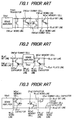
- FIGs.1 to 3 Before explaining a ferroelectric memory device in the preferred embodiments according to the invention, the aforementioned conventional ferroelectric memory device will be explained referring to FIGs.1 to 3.
- a ferroelectric memory device employing a memory cell of one transistor - one capacitor type (a 1T1C - type)
- a reference voltage in order to discriminate whether a datum read from a memory cell is "0" or "1" .
- a technology using a dummy cell is well known.
- methods for constructing the dummy cell those disclosed on Japanese Patent Kokai 7-192476 and 7-93978 can be enumerated. In these methods, two dummy cells respectively comprising ferroelectric capacitors are set up, and data "1" and "0” are respectively written in both the dummy cells. The reference voltage generated by reading these data and deriving the mean value of them.
- TSW1 is made to be off, and the bit line BLa1 is again pre-charged and a datum stored in the memory cell MCa1 is read.
- the voltage of the bit line BLa1 corresponds to a datum read from the memory cell MCa1, i.e. "1" and "0"
- the voltage of the bit line BLa2 corresponds to a datum intermediate between "1" and "0” .
- a ferroelectric memory device of a one transistor - one capacitance type an be constructed.
- a reference voltage generated by the dummy cell is stored in a memory, and thereafter the reference voltage is not generated by the dummy cell, and thereby, the deterioration of the dummy cell caused by dielectric fatigue of ferroelectric material can be prevented.
- a memory cell MCa1 is selected by a word line WLa1, and a signal voltage is generated on a bit line BLa1 by driving a plate line PLa1.
- a dummy cell DMCa1 is selected by a word line DWLa1, and a reference voltage is generated on a bit line BLa2 by driving a plate line DPLa1.
- the capacitor size of the dummy cell is so selected that it is smaller than that of the memory cell, and the direction of its polarization is so set that the polarization is always inverted, whenever the reference voltage is generate.
- the capacitance of CFa1 in case that its polarization is not inverted is smaller than the capacitance of DCFa1 in case that its polarization is inverted.
- the capacitance of DCFa1 is smaller than that of CFa1 in case that its polarization is inverted, and larger than that of CFa1 in case that its polarization is not inverted. Accordingly, a signal voltage corresponding to a datum intermediate between "1" and "0" can be generated on the bit line BLa2.
- the capacitor size of the DCFa1 is smaller than that of CFa1, but a similar result can be obtained in case that the capacitor size of DCFa1 is larger than that of CFa1, and the direction of polarization of the dummy cell is set so that it is not inverted in case that the reference voltage is generated, as shown in U.S. patent 4873664.
- a capacitor comprising ordinary dielectric material is used as a dummy cell, and a signal voltage obtained by reading a memory cell is raised by using electric charge stored in the dummy cell so that a pre-charge voltage is equal to a voltage corresponding to an intermediate level between "1" and "0" .
- a voltage VCC/2 is applied between both the electrodes of the memory cell capacitor CFa1 from the outside.
- a memory cell MCa1 is selected by a word line WLa1, and a signal voltage is generated on a bit line BLa1.
- a dummy cell capacitor DCa1 is selected by a dummy cell word line DWLa1 and the voltage of the bit line BLa1 is raised.
- a dummy cell word line DWLa1 is selected, and the voltage of the bit line is raised.
- the capacitance of the dummy cell is so selected that, the raised voltage of the bit line is higher than the pre-charge voltage in case that the datum is "1" , and lower than the pre-charge voltage in case that the datum is "0".
- the datum can be detected by means of a sense amplifier SAa1 using the pre-charge voltage of BLa2 as the reference voltage.
- the capacitance of the memory cell capacitor is previously estimated, thereafter the capacitance of the dummy cell is estimated in both cases that the polarization of the dummy cell is inverted and not inverted, and the capacitor size of the dummy cell is determined based on the aforementioned estimations, so that it is difficult to design the capacitor size of the dummy cell.
- the capacitor size of the dummy cell is determined based on the aforementioned estimations, so that it is difficult to design the capacitor size of the dummy cell.
- third dummy cell shown in FIG.3 in which a capacitor comprising ordinary dielectric material is used as a dummy cell, a similar problem occurs also.
- FIG.4 shows the first preferred embodiment of the invention, which is a fundamental circuit structure related to a non-volatile semiconductor memory device according to the invention.
- a sense amplifier SA1 which detects a datum by amplifying a voltage difference between both the bit lines, are connected with their ends.
- PMOS transistors T1 and T2 are connected in parallel with PMOS transistors of a conventional latch type sense amplifier.
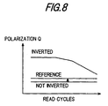
- the widths W of the channels of PMOS transistors T1 and T2 are so selected that a slight offset is introduced into the sense amplifier SA1 and an apparent reference voltage is slightly higher than a voltage read on the bit line in case that the polarization of a dummy cell is not inverted as shown in FIG.8.
- a memory cell MC1 is composed of a ferroelectric capacitor CF1 and a cell transistor TC1.
- a terminal of the ferroelectric capacitor CF1 is connected with a plate line PL1, and the other terminal thereof is connected with one of source and drain terminals of the cell transistor TC1.
- the other terminal in the source and drain terminals of the cell transistor TC1 is connected with the bit line BL1, and a gate terminal is connected with a word line WL1.
- the other memory cell MC2 and dummy cells DMC1 and DMC2 have the same circuit structures as that of the memory cell MC1, and the sizes of the structural elements are the same as those of the memory cell MC1.
- the operation of the circuit shown in FIG.4 for reading data stored in a memory cell will be explained.
- the dummy cell capacitors DCF1 and DCF2 the directions of the polarizations are previously set so that the polarizations are not inverted in case data stored therein are read.
- the bit lines BL1 and BL2 are pre-charged at the ground voltage.
- the memory MC1 is selected by applying "H" level to the word line WL1, and a datum of the memory cell MC1 is read on the bit line BL1 by applying "H" level to the plate line PL1.
- a dummy cell DMC2 is selected by applying "H" level to the word line DWL2, and a charge, which corresponds to case that the polarization is not inverted, is read on the bit line BL2 by applying "H" level to the plate line DPL2. Then, the PMOS transistor T1 is made to be off and the transistor T2 is made to be on in order to make the sense amplifier SA1 be unbalanced, and the sense amplifier SA1 is activated.
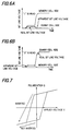
- the reference voltage is apparently higher than a voltage read on the bit line connected with the memory cell, the polarization of which is not inverted, and lower than a voltage read on the bit line connected with the memory cell, the polarization of which is inverted, as shown in FIG.8. Then, the voltages of the bit lines BL1 and BL2 will be considered. In case that the polarization of the memory cell is inverted, the bit line on the memory cell side is at high level and the bit line on the dummy cell side is at low level as shown in FIG.6A.
- the bit line on the memory cell side is at low level, and the bit line on the dummy cell side is at high level as shown in FIG.6B. Accordingly a datum in the memory cell MC1 can be exactly read. Moreover, since the polarization of the dummy cell is not inverted in case that the datum stored in the dummy cell is read, the problem of dielectric fatigue, which occurs in case that the polarization is repeatedly inverted, in other words, the uncertainty of the reference voltage, which is caused by the difference in the number of access between the memory cell and the dummy cell, is out of the question.
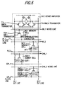
- FIG.5 shows the second preferred embodiment of the invention.
- the structures of the memory cell and the dummy cell are the same as those shown in the first preferred embodiment.
- a sense amplifier SA2 is set at the ends of bit lines BL1 and BL2, and NMOS transistors T3 and T4 are connected in parallel with NMOS transistors of the conventional latch type sense amplifier.
- the operation of the circuit shown in FIG.5 for reading a datum stored in the memory cell will be explained.
- the directions of the polarizations of the dummy cells DMC1 and DMC2 are previously set so that the polarizations are not inverted in case that data stored therein are read.
- the bit lines BL1 and BL2 are pre-charged at the ground voltage.
- a memory cell MC1 is selected by applying "H" level to the word line WL1, and a datum in the memory cell MC1 is read on the bit line BL1 by applying "H" level to a plate line PL1.
- a dummy cell DMC2 is selected by applying "H" level to a word line DWL2, and a charge, which corresponds to case that the polarization of the dummy cell DMC2 is not inverted, is read on the bit line BL2 by applying "H" level to a plate line DPL2. Thereafter, a NMOS transistor T3 is made to be on and a NMOS transistor T4 is made to be off in order to make the sense amplifier SA2 be unbalanced, and the sense amplifier SA2 is activated.
- the apparent voltage of the bit line BL2 is higher than a voltage read on the bit line BL1 in case that the polarization of the memory is not inverted, and lower than the voltage read on the bit line BL1 in case that the polarization of the memory cell is inverted, so that a datum in the memory cell can be exactly read.
- the polarization of the dummy cell is not inverted in case that the datum stored therein is read, the uncertainty of the reference voltage, which is caused by the difference in the number of access between the memory cell and the dummy cell, is out of the question.
- the polarization of the dummy cell is not inverted in case that the datum stored therein is read, dielectric fatigue of the dummy cell capacitor can be suppressed, and the uncertainty of the reference voltage, which is caused by the difference in the number of access between the memory cell and the dummy cell, can be eliminated.
- the capacitor size of the dummy cell is equal to that of the memory cell, the design of the capacitor size can be simplified.
Landscapes
- Engineering & Computer Science (AREA)
- Computer Hardware Design (AREA)
- Dram (AREA)
- Read Only Memory (AREA)
Applications Claiming Priority (3)
| Application Number | Priority Date | Filing Date | Title |
|---|---|---|---|
| JP19120797 | 1997-07-16 | ||
| JP191207/97 | 1997-07-16 | ||
| JP19120797A JP3196824B2 (ja) | 1997-07-16 | 1997-07-16 | 強誘電体メモリ装置 |
Publications (3)
| Publication Number | Publication Date |
|---|---|
| EP0892408A2 true EP0892408A2 (fr) | 1999-01-20 |
| EP0892408A3 EP0892408A3 (fr) | 2000-08-16 |
| EP0892408B1 EP0892408B1 (fr) | 2003-06-18 |
Family
ID=16270693
Family Applications (1)
| Application Number | Title | Priority Date | Filing Date |
|---|---|---|---|
| EP98113296A Expired - Lifetime EP0892408B1 (fr) | 1997-07-16 | 1998-07-16 | Dispositif de mémoire ferroélectrique |
Country Status (6)
| Country | Link |
|---|---|
| US (1) | US5926413A (fr) |
| EP (1) | EP0892408B1 (fr) |
| JP (1) | JP3196824B2 (fr) |
| KR (1) | KR100293622B1 (fr) |
| DE (1) | DE69815600T2 (fr) |
| TW (1) | TW388876B (fr) |
Cited By (3)
| Publication number | Priority date | Publication date | Assignee | Title |
|---|---|---|---|---|
| WO2004047117A1 (fr) * | 2002-11-20 | 2004-06-03 | Infineon Technologies Ag | Mode d'essai pour mesurer la marge de signaux dans une configuration de type 2t2c au moyen d'une charge et decharge specifiques de lignes de bits (bl) |
| WO2004047118A1 (fr) * | 2002-11-20 | 2004-06-03 | Infineon Technologies Ag | Mode d'essai de marge de signal 2t2c dans lequel il est fait appel a un element resistif |
| US6876590B2 (en) | 2002-11-20 | 2005-04-05 | Infineon Technologies, Ag | 2T2C signal margin test mode using a defined charge exchange between BL and/BL |
Families Citing this family (37)
| Publication number | Priority date | Publication date | Assignee | Title |
|---|---|---|---|---|
| JPH11273360A (ja) * | 1998-03-17 | 1999-10-08 | Toshiba Corp | 強誘電体記憶装置 |
| JPH11273362A (ja) * | 1998-03-18 | 1999-10-08 | Sharp Corp | 不揮発性半導体記憶装置 |
| KR100363102B1 (ko) * | 1998-07-15 | 2003-02-19 | 주식회사 하이닉스반도체 | 강유전체 메모리 |
| JP4490514B2 (ja) * | 1998-10-08 | 2010-06-30 | 株式会社東芝 | 強誘電体メモリ |
| KR100296917B1 (ko) * | 1999-06-28 | 2001-07-12 | 박종섭 | 강유전체 메모리 소자의 기준 전압 발생 장치 |
| KR100333702B1 (ko) * | 1999-06-28 | 2002-04-24 | 박종섭 | 강유전체 메모리 장치 |
| JP3703655B2 (ja) * | 1999-08-11 | 2005-10-05 | 株式会社東芝 | タイミング信号発生回路 |
| JP3551858B2 (ja) | 1999-09-14 | 2004-08-11 | 日本電気株式会社 | 半導体メモリ装置 |
| KR100348576B1 (ko) | 1999-09-30 | 2002-08-13 | 동부전자 주식회사 | 강유전체 메모리 |
| KR100348577B1 (ko) | 1999-09-30 | 2002-08-13 | 동부전자 주식회사 | 강유전체 메모리 |
| US6573772B1 (en) * | 2000-06-30 | 2003-06-03 | Intel Corporation | Method and apparatus for locking self-timed pulsed clock |
| JP2002197854A (ja) | 2000-12-22 | 2002-07-12 | Matsushita Electric Ind Co Ltd | 強誘電体メモリ装置 |
| JP4329919B2 (ja) * | 2001-03-13 | 2009-09-09 | Okiセミコンダクタ株式会社 | 半導体メモリおよび半導体メモリの駆動方法 |
| KR100460767B1 (ko) * | 2001-12-20 | 2004-12-09 | 주식회사 하이닉스반도체 | 강유전체 메모리 소자의 기준전압 발생장치 |
| JP4161951B2 (ja) | 2004-09-16 | 2008-10-08 | セイコーエプソン株式会社 | 強誘電体メモリ装置 |
| JP4470889B2 (ja) | 2006-01-25 | 2010-06-02 | セイコーエプソン株式会社 | 分極転送デバイス、及びその転送制御方法 |
| JP4983062B2 (ja) * | 2006-03-20 | 2012-07-25 | 富士通セミコンダクター株式会社 | メモリ装置 |
| US7649793B1 (en) | 2006-05-04 | 2010-01-19 | Marvell International Ltd. | Channel estimation for multi-level memories using pilot signals |
| US8645793B2 (en) * | 2008-06-03 | 2014-02-04 | Marvell International Ltd. | Statistical tracking for flash memory |
| KR100715979B1 (ko) * | 2006-05-25 | 2007-05-08 | 경북대학교 산학협력단 | 피형 금속 산화막 반도체 게이팅 셀을 이용한 강유전체메모리 |
| US7808834B1 (en) | 2007-04-13 | 2010-10-05 | Marvell International Ltd. | Incremental memory refresh |
| US8031526B1 (en) | 2007-08-23 | 2011-10-04 | Marvell International Ltd. | Write pre-compensation for nonvolatile memory |
| US8189381B1 (en) | 2007-08-28 | 2012-05-29 | Marvell International Ltd. | System and method for reading flash memory cells |
| US8085605B2 (en) | 2007-08-29 | 2011-12-27 | Marvell World Trade Ltd. | Sequence detection for flash memory with inter-cell interference |
| US9911501B2 (en) * | 2016-05-24 | 2018-03-06 | Silicon Storage Technology, Inc. | Sensing amplifier comprising a built-in sensing offset for flash memory devices |
| US9899073B2 (en) | 2016-06-27 | 2018-02-20 | Micron Technology, Inc. | Multi-level storage in ferroelectric memory |
| US11482529B2 (en) | 2019-02-27 | 2022-10-25 | Kepler Computing Inc. | High-density low voltage non-volatile memory with unidirectional plate-line and bit-line and pillar capacitor |
| US10998025B2 (en) | 2019-02-27 | 2021-05-04 | Kepler Computing, Inc. | High-density low voltage non-volatile differential memory bit-cell with shared plate-line |
| JP2020155187A (ja) | 2019-03-22 | 2020-09-24 | ソニーセミコンダクタソリューションズ株式会社 | 強誘電体メモリおよびそのメモリ素子 |
| US10964357B2 (en) * | 2019-04-24 | 2021-03-30 | Marvell Asia Pte., Ltd. | Skewed sense amplifier for single-ended sensing |
| US11527277B1 (en) | 2021-06-04 | 2022-12-13 | Kepler Computing Inc. | High-density low voltage ferroelectric memory bit-cell |
| US11729991B1 (en) | 2021-11-01 | 2023-08-15 | Kepler Computing Inc. | Common mode compensation for non-linear polar material based differential memory bit-cell |
| US11482270B1 (en) | 2021-11-17 | 2022-10-25 | Kepler Computing Inc. | Pulsing scheme for a ferroelectric memory bit-cell to minimize read or write disturb effect and refresh logic |
| US12108609B1 (en) | 2022-03-07 | 2024-10-01 | Kepler Computing Inc. | Memory bit-cell with stacked and folded planar capacitors |
| US20230395134A1 (en) | 2022-06-03 | 2023-12-07 | Kepler Computing Inc. | Write disturb mitigation for non-linear polar material based multi-capacitor bit-cell |
| US12347476B1 (en) | 2022-12-27 | 2025-07-01 | Kepler Computing Inc. | Apparatus and method to improve sensing noise margin in a non-linear polar material based bit-cell |
| US12334127B2 (en) | 2023-01-30 | 2025-06-17 | Kepler Computing Inc. | Non-linear polar material based multi-capacitor high density bit-cell |
Family Cites Families (10)
| Publication number | Priority date | Publication date | Assignee | Title |
|---|---|---|---|---|
| JPH0713877B2 (ja) * | 1988-10-19 | 1995-02-15 | 株式会社東芝 | 半導体メモリ |
| JP3169599B2 (ja) * | 1990-08-03 | 2001-05-28 | 株式会社日立製作所 | 半導体装置、その駆動方法、その読み出し方法 |
| US5461713A (en) * | 1991-05-10 | 1995-10-24 | Sgs-Thomson Microelectronics S.R.L. | Current offset sense amplifier of a modulated current or current unbalance type for programmable memories |
| US5539279A (en) * | 1993-06-23 | 1996-07-23 | Hitachi, Ltd. | Ferroelectric memory |
| JP3186485B2 (ja) * | 1995-01-04 | 2001-07-11 | 日本電気株式会社 | 強誘電体メモリ装置およびその動作制御方法 |
| JPH097377A (ja) * | 1995-06-20 | 1997-01-10 | Sony Corp | 強誘電体記憶装置 |
| EP0767464B1 (fr) * | 1995-09-08 | 2003-11-19 | Fujitsu Limited | Mémoire ferro-électrique et méthode de lecture de données à partir de cette mémoire |
| US5677865A (en) * | 1995-09-11 | 1997-10-14 | Micron Technology, Inc. | Ferroelectric memory using reference charge circuit |
| JPH09134594A (ja) * | 1995-11-08 | 1997-05-20 | Hitachi Ltd | 半導体不揮発メモリ |
| US5764561A (en) * | 1995-11-16 | 1998-06-09 | Rohm Co., Ltd. | Ferroelectric memory devices and method of using ferroelectric capacitors |
-
1997
- 1997-07-16 JP JP19120797A patent/JP3196824B2/ja not_active Expired - Fee Related
-
1998
- 1998-07-14 KR KR1019980028393A patent/KR100293622B1/ko not_active Expired - Fee Related
- 1998-07-15 US US09/115,344 patent/US5926413A/en not_active Expired - Lifetime
- 1998-07-16 TW TW087111633A patent/TW388876B/zh not_active IP Right Cessation
- 1998-07-16 EP EP98113296A patent/EP0892408B1/fr not_active Expired - Lifetime
- 1998-07-16 DE DE69815600T patent/DE69815600T2/de not_active Expired - Fee Related
Cited By (4)
| Publication number | Priority date | Publication date | Assignee | Title |
|---|---|---|---|---|
| WO2004047117A1 (fr) * | 2002-11-20 | 2004-06-03 | Infineon Technologies Ag | Mode d'essai pour mesurer la marge de signaux dans une configuration de type 2t2c au moyen d'une charge et decharge specifiques de lignes de bits (bl) |
| WO2004047118A1 (fr) * | 2002-11-20 | 2004-06-03 | Infineon Technologies Ag | Mode d'essai de marge de signal 2t2c dans lequel il est fait appel a un element resistif |
| US6826099B2 (en) | 2002-11-20 | 2004-11-30 | Infineon Technologies Ag | 2T2C signal margin test mode using a defined charge and discharge of BL and /BL |
| US6876590B2 (en) | 2002-11-20 | 2005-04-05 | Infineon Technologies, Ag | 2T2C signal margin test mode using a defined charge exchange between BL and/BL |
Also Published As
| Publication number | Publication date |
|---|---|
| DE69815600T2 (de) | 2004-04-29 |
| JPH1139882A (ja) | 1999-02-12 |
| JP3196824B2 (ja) | 2001-08-06 |
| US5926413A (en) | 1999-07-20 |
| EP0892408B1 (fr) | 2003-06-18 |
| TW388876B (en) | 2000-05-01 |
| KR100293622B1 (ko) | 2001-07-12 |
| DE69815600D1 (de) | 2003-07-24 |
| EP0892408A3 (fr) | 2000-08-16 |
| KR19990013853A (ko) | 1999-02-25 |
Similar Documents
| Publication | Publication Date | Title |
|---|---|---|
| EP0892408B1 (fr) | Dispositif de mémoire ferroélectrique | |
| US6493251B2 (en) | Ferroelectric memory device | |
| KR100324594B1 (ko) | 강유전체 메모리 장치 | |
| EP0926685B1 (fr) | Dispositif de mémoire ferroélectrique ayant un circuit de lecture à haute vitesse | |
| CN100468566C (zh) | 铁电存储器件 | |
| EP1349173B1 (fr) | Dispositif de mémoire à semiconducteurs et sa méthode de commande | |
| KR100323985B1 (ko) | 반도체 기억 장치 | |
| US6026009A (en) | Ferroelectric memory device increasing voltage on a bit line to remove dummy cells and a reference voltage generator | |
| US6623989B2 (en) | Nonvolatile ferroelectric memory and method for fabricating the same | |
| US6046928A (en) | Non-volatile semiconductor memory device | |
| KR100338552B1 (ko) | 불휘발성 강유전체 랜덤 액세스 메모리 장치 및 그것의 데이터읽기 방법 | |
| US6795330B2 (en) | Method of reading and restoring data stored in a ferroelectric memory cell | |
| KR19980087512A (ko) | 하나의 메모리셀에 다수비트의 정보를 저장할 수 있는 반도체 기억장치 | |
| US7106615B2 (en) | FeRAM capable of restoring “0” data and “1” data at a time | |
| KR100363102B1 (ko) | 강유전체 메모리 | |
| US6574134B1 (en) | Non-volatile ferroelectric capacitor memory circuit having nondestructive read capability | |
| US20090059648A1 (en) | Ferroelectric semiconductor storage device | |
| JP3467353B2 (ja) | データ記憶装置 | |
| US6442059B1 (en) | Nonvolatile ferroelectric memory and method for fabricating the same | |
| KR100333697B1 (ko) | 강유전체기억소자 | |
| KR100275338B1 (ko) | 강유전체 메모리의 기준전압발생기 | |
| JPH11102980A (ja) | FeRAMセル及びその書込方法並びにこのセルを用いたFeRAMセルアレイ及びFeRAM | |
| KR100744687B1 (ko) | 강유전체의 분극 상태에 따라 문턱전압이 조절되는 트랜지스터를 구비하는 강유전체 메모리 소자의 레퍼런스 회로 | |
| KR100318423B1 (ko) | 강유전체 메모리 장치 | |
| KR100255515B1 (ko) | 강유전체 메모리 소자 |
Legal Events
| Date | Code | Title | Description |
|---|---|---|---|
| PUAI | Public reference made under article 153(3) epc to a published international application that has entered the european phase |
Free format text: ORIGINAL CODE: 0009012 |
|
| AK | Designated contracting states |
Kind code of ref document: A2 Designated state(s): DE FR |
|
| AX | Request for extension of the european patent |
Free format text: AL;LT;LV;MK;RO;SI |
|
| PUAL | Search report despatched |
Free format text: ORIGINAL CODE: 0009013 |
|
| AK | Designated contracting states |
Kind code of ref document: A3 Designated state(s): AT BE CH CY DE DK ES FI FR GB GR IE IT LI LU MC NL PT SE |
|
| AX | Request for extension of the european patent |
Free format text: AL;LT;LV;MK;RO;SI |
|
| 17P | Request for examination filed |
Effective date: 20001206 |
|
| AKX | Designation fees paid |
Free format text: DE FR |
|
| GRAH | Despatch of communication of intention to grant a patent |
Free format text: ORIGINAL CODE: EPIDOS IGRA |
|
| GRAH | Despatch of communication of intention to grant a patent |
Free format text: ORIGINAL CODE: EPIDOS IGRA |
|
| GRAH | Despatch of communication of intention to grant a patent |
Free format text: ORIGINAL CODE: EPIDOS IGRA |
|
| GRAA | (expected) grant |
Free format text: ORIGINAL CODE: 0009210 |
|
| RAP1 | Party data changed (applicant data changed or rights of an application transferred) |
Owner name: NEC ELECTRONICS CORPORATION |
|
| AK | Designated contracting states |
Designated state(s): DE FR |
|
| REF | Corresponds to: |
Ref document number: 69815600 Country of ref document: DE Date of ref document: 20030724 Kind code of ref document: P |
|
| ET | Fr: translation filed | ||
| PLBE | No opposition filed within time limit |
Free format text: ORIGINAL CODE: 0009261 |
|
| STAA | Information on the status of an ep patent application or granted ep patent |
Free format text: STATUS: NO OPPOSITION FILED WITHIN TIME LIMIT |
|
| 26N | No opposition filed |
Effective date: 20040319 |
|
| PGFP | Annual fee paid to national office [announced via postgrant information from national office to epo] |
Ref country code: FR Payment date: 20040708 Year of fee payment: 7 |
|
| PGFP | Annual fee paid to national office [announced via postgrant information from national office to epo] |
Ref country code: DE Payment date: 20040729 Year of fee payment: 7 |
|
| PG25 | Lapsed in a contracting state [announced via postgrant information from national office to epo] |
Ref country code: DE Free format text: LAPSE BECAUSE OF NON-PAYMENT OF DUE FEES Effective date: 20060201 |
|
| PG25 | Lapsed in a contracting state [announced via postgrant information from national office to epo] |
Ref country code: FR Free format text: LAPSE BECAUSE OF NON-PAYMENT OF DUE FEES Effective date: 20060331 |
|
| REG | Reference to a national code |
Ref country code: FR Ref legal event code: ST Effective date: 20060331 |