EP0892425A2 - Fabriciation method for a platinum-metal pattern by means of a lift-off process - Google Patents
Fabriciation method for a platinum-metal pattern by means of a lift-off process Download PDFInfo
- Publication number
- EP0892425A2 EP0892425A2 EP98105612A EP98105612A EP0892425A2 EP 0892425 A2 EP0892425 A2 EP 0892425A2 EP 98105612 A EP98105612 A EP 98105612A EP 98105612 A EP98105612 A EP 98105612A EP 0892425 A2 EP0892425 A2 EP 0892425A2
- Authority
- EP
- European Patent Office
- Prior art keywords
- mask
- layer
- platinum metal
- silicon oxide
- substrate
- Prior art date
- Legal status (The legal status is an assumption and is not a legal conclusion. Google has not performed a legal analysis and makes no representation as to the accuracy of the status listed.)
- Ceased
Links
Images
Classifications
-
- H—ELECTRICITY
- H10—SEMICONDUCTOR DEVICES; ELECTRIC SOLID-STATE DEVICES NOT OTHERWISE PROVIDED FOR
- H10D—INORGANIC ELECTRIC SEMICONDUCTOR DEVICES
- H10D1/00—Resistors, capacitors or inductors
- H10D1/60—Capacitors
- H10D1/68—Capacitors having no potential barriers
- H10D1/692—Electrodes
-
- H—ELECTRICITY
- H10—SEMICONDUCTOR DEVICES; ELECTRIC SOLID-STATE DEVICES NOT OTHERWISE PROVIDED FOR
- H10D—INORGANIC ELECTRIC SEMICONDUCTOR DEVICES
- H10D1/00—Resistors, capacitors or inductors
- H10D1/60—Capacitors
- H10D1/68—Capacitors having no potential barriers
- H10D1/692—Electrodes
- H10D1/694—Electrodes comprising noble metals or noble metal oxides
-
- H—ELECTRICITY
- H10—SEMICONDUCTOR DEVICES; ELECTRIC SOLID-STATE DEVICES NOT OTHERWISE PROVIDED FOR
- H10P—GENERIC PROCESSES OR APPARATUS FOR THE MANUFACTURE OR TREATMENT OF DEVICES COVERED BY CLASS H10
- H10P14/00—Formation of materials, e.g. in the shape of layers or pillars
- H10P14/60—Formation of materials, e.g. in the shape of layers or pillars of insulating materials
- H10P14/69—Inorganic materials
- H10P14/692—Inorganic materials composed of oxides, glassy oxides or oxide-based glasses
- H10P14/6921—Inorganic materials composed of oxides, glassy oxides or oxide-based glasses containing silicon
- H10P14/69215—Inorganic materials composed of oxides, glassy oxides or oxide-based glasses containing silicon the material being a silicon oxide, e.g. SiO2
-
- H—ELECTRICITY
- H10—SEMICONDUCTOR DEVICES; ELECTRIC SOLID-STATE DEVICES NOT OTHERWISE PROVIDED FOR
- H10P—GENERIC PROCESSES OR APPARATUS FOR THE MANUFACTURE OR TREATMENT OF DEVICES COVERED BY CLASS H10
- H10P50/00—Etching of wafers, substrates or parts of devices
- H10P50/20—Dry etching; Plasma etching; Reactive-ion etching
- H10P50/28—Dry etching; Plasma etching; Reactive-ion etching of insulating materials
Definitions
- the invention relates to a manufacturing method for a platinum metal structure on a substrate, especially during manufacture an integrated circuit.
- platinum metals as conductive materials is becoming increasingly interesting in semiconductor technology. Under Platinum metal "is to be understood as the group of platinum metals, ie Pt, Ir, Ru etc. As noble metals they have a high conductivity and do not form non-conductive oxides even at high temperatures in an oxygen-containing atmosphere. Furthermore, they have good interface properties both mechanically and An important area of application of platinum metals is the use as an electrode material for storage capacitors in integrated DRAM memories, in particular if these contain a so-called high- ⁇ dielectric (for example BST) or a ferroelectric as a storage dielectric The production of these storage dielectrics requires high temperatures in an oxidizing atmosphere, and such storage cells require little space and are very interesting for future storage generations.
- high- ⁇ dielectric for example BST
- ferroelectric ferroelectric
- platinum metals are difficult to etch are.
- Previous methods are based mainly on physical Etching, for example ion milling and therefore have low selectivity to other materials, such as for example photoresist. For larger structures too already lift-off with a mask made of photoresist or Titan used.
- a lift-off procedure is carried out under the structuring layer applied a mask to a substrate, the one at the locations of the structure to be created Opening included. Only the part lying on the mask the layer is then removed along with the mask.
- the mask at the edge of the opening is negative Has flank
- the exposed substrate surface is larger than the mask opening at the top of the mask.
- the mask must be overhanging in some form be. This means that the flank is not coated and the solvent for the mask can attack at this point.
- photoresist as a mask in a lift-off procedure are these negative edges only for semiconductor manufacturing unusual special procedures (e.g. Image reversal).
- titanium When using titanium as The time factor plays an important role in the mask, since titanium Contact with air slightly oxidized on the surface and then is difficult to remove.
- the object of the invention is a simple manufacturing process for a structure made of a platinum metal.
- the Manufacturing process should also in the manufacturing process DRAM memory cell can be integrated.
- the invention is based on the use of silicon oxide Part of a mask for a lift-off process. Doing so the required negative edge of the mask according to a first Embodiment achieved by an etching process, in particular through a combination of an anisotropic and a isotropic etching process.
- a silicon layer is applied to the silicon oxide layer and after structuring this double layer accordingly oxidation of the silicon layer of the mask to be produced carried out; the resulting increase in volume Silicon layer leads to an overhang over the silicon oxide layer.
- the silicon oxide mask can be very simple, for example with HF, be removed.
- DRAM memory cell can be integrated, in which an electrode of the Storage capacitor is made of a platinum metal.
- an etch stop layer for example, in front of the silicon oxide layer of silicon nitride to be applied to the Protect removal of the mask.
- Preferred is platinum metal Pt or Ir used.
- a substrate 1 is made of nitride, for example Etch stop layer 2, a silicon oxide layer 3 and one Mask layer 4 applied using known methods.
- the thicknesses of layers 2 and 3 can be, for example, 20 nm and 50 nm.
- the substrate can be completed circuit elements included, for example an electrical Connection for the platinum structure to be produced.
- the optional The etch stop layer preferably consists of silicon nitride.
- the Mask layer 4 can either be a photoresist layer, the exposed according to the platinum structure to be produced and is developed so that it can be manufactured in the field Platinum structure has an opening.
- the hard mask 4 can also be one be a so-called hard mask, which consists for example of silicon nitride, and that with the help of an appropriately structured additional Photo mask 4 '(shown in dashed lines) is generated.
- the hard mask 4 after removal the paint mask 4 'used as mask 4.
- the platinum metal also can be sputtered hot.
- the silicon oxide layer 3 etched.
- the oxide layer 3 is initially anisotropic up to the etch stop layer 2 etched.
- the exposed etch stop layer is removed so that the substrate - possibly with a connection structure for the platinum structure - exposed.
- This arrangement is the whole area a platinum metal 5, preferably Pt, for example through a sputtering process.
- the edges of the silicon oxide mask 3 are not coated, so that in subsequent silicon oxide wet etching process to the solvent can attack these places and that on the mask surface overlying platinum is also removed.
- a storage capacitor can pass through Application of a storage dielectric 6, in particular one high ⁇ dielectric or a ferroelectric as explained above, and then producing a second capacitor electrode 7 (also made of platinum, for example) become.
- FIG 5 In the second embodiment, as in the first Embodiment preferably first an etch stop layer 2 applied to the substrate 1. This creates a double layer deposited from silicon oxide 3 and polysilicon 8. Subsequently, an oxidation protection layer 9, in particular a nitride layer. The sequence of layers 3, 8, 9 is then attached using a photo mask 4 an opening in the place of the platinum structure to be produced has anisotropically etched up to the etch stop layer 2. The Paint mask 4 can then be removed.
- a thermal oxidation is carried out the polysilicon at the exposed locations with an increase in volume converted to silicon oxide. This will open up reduced in size in the polysilicon layer 8 and it is formed an overhang over the silicon oxide structure.
- the mask for the The lift-off process here consists of the silicon oxide layer and the polysilicon layer (and possibly the nitride layer).
- the optional oxidation protection layer 9 causes a larger one Overhang, since then the polysilicon 8 only on the exposed Can oxidize edges. In this embodiment In any case, the layout must take into account that due to the oxidation opens up from the original Paint mask 4 is reduced.
- the further process can be done here in the first embodiment be carried out, i.e. it becomes the etch stop layer 2 removed, then applied a platinum metal and that on the Platinum metal on the mask surface together with the Mask removed. As explained, a capacitor can then be used to get finished.
Landscapes
- Semiconductor Memories (AREA)
- Preparing Plates And Mask In Photomechanical Process (AREA)
- Non-Volatile Memory (AREA)
- Electrodes Of Semiconductors (AREA)
- Internal Circuitry In Semiconductor Integrated Circuit Devices (AREA)
- Semiconductor Integrated Circuits (AREA)
Abstract
Das Herstellverfahren beinhaltet für die Strukturierung des
Platinmetalls ein Lift-off-Verfahren, bei dem die Maske eine
Siliziumoxidschicht enthält. Durch die Verwendung von Siliziumoxid
kann eine erforderliche negative Flanke der Maske
erzielt werden und die Maske kann einfach entfernt werden.
Das Verfahren kann bei der Herstellung von DRAMs mit einem
hoch-ε-Dielektrikum und FRAM's eingesetzt werden.
Description
Die Erfindung betrifft ein Herstellverfahren für eine Platinmetall-Struktur auf einem Substrat, insbesondere bei der Herstellung einer integrierten Schaltung.The invention relates to a manufacturing method for a platinum metal structure on a substrate, especially during manufacture an integrated circuit.
In der Halbleitertechnologie wird die Verwendung von Platinmetallen
als leitenden Materialien zunehmend interessant. Unter
![]()
![]()
Ein Nachteil der Platinmetalle ist, daß sie schwer ätzbar sind. Bisherige Verfahren beruhen auf überwiegend physikalischer Ätzung, beispielsweise Ion Milling und besitzen daher nur geringe Selektivität gegenüber anderen Materialien, wie beispielsweise Fotolack. Für größere Strukturen wurden auch bereits Lift-off-Verfahren mit einer Maske aus Fotolack oder Titan verwendet. A disadvantage of platinum metals is that they are difficult to etch are. Previous methods are based mainly on physical Etching, for example ion milling and therefore have low selectivity to other materials, such as for example photoresist. For larger structures too already lift-off with a mask made of photoresist or Titan used.
Bei einem Lift-off-Verfahren wird bekanntermaßen unter der zu strukturierenden Schicht eine Maske auf ein Substrat aufgebracht, die an den Stellen der zu erzeugenden Struktur eine Öffnung enthalt. Lediglich der auf der Maske aufliegende Teil der Schicht wird dann zusammen mit der Maske entfernt. Dabei ist wichtig, daß die Maske am Rand der Öffnung eine negative Flanke aufweist, die freiliegende Substratoberfläche also größer ist als die Maskenöffnung an der Oberseite der Maske. Mit anderen Worten, die Maske muß in irgendeiner Form überhängend sein. Dadurch wird die Flanke nicht beschichtet und das Lösungsmittel für die Maske kann an dieser Stelle angreifen. Bei Verwendung von Fotolack als Maske in einem Lift-off-Verfahren sind diese negativen Flanken nur mit für die Halbleiterfertigung unüblichen Spezialverfahren (beispielsweise Image-Reversal) zu erreichen. Bei Verwendung von Titan als Maske spielt der Zeitfaktor eine wichtige Rolle, da Titan bei Kontakt mit Luft leicht an der Oberfläche oxidiert und dann schlecht zu entfernen ist.As is known, a lift-off procedure is carried out under the structuring layer applied a mask to a substrate, the one at the locations of the structure to be created Opening included. Only the part lying on the mask the layer is then removed along with the mask. Here it is important that the mask at the edge of the opening is negative Has flank, the exposed substrate surface is larger than the mask opening at the top of the mask. In other words, the mask must be overhanging in some form be. This means that the flank is not coated and the solvent for the mask can attack at this point. When using photoresist as a mask in a lift-off procedure are these negative edges only for semiconductor manufacturing unusual special procedures (e.g. Image reversal). When using titanium as The time factor plays an important role in the mask, since titanium Contact with air slightly oxidized on the surface and then is difficult to remove.
Die Erfindung hat zur Aufgabe, ein einfaches Herstellverfahren für eine Struktur aus einem Platinmetall anzugeben. Das Herstellverfahren soll ferner in den Herstellprozeß einer DRAM-Speicherzelle integrierbar sein.The object of the invention is a simple manufacturing process for a structure made of a platinum metal. The Manufacturing process should also in the manufacturing process DRAM memory cell can be integrated.
Diese Aufgabe wird durch ein Verfahren mit den Merkmalen des
Patentanspruchs 1 und durch ein Verfahren mit den Merkmalen
des Patentanspruchs 2 gelöst.This task is accomplished by a process with the characteristics of
Claim 1 and by a method with the features
of
Die Erfindung beruht auf der Verwendung von Siliziumoxid als Bestandteil einer Maske für einen Lift-off-Prozeß. Dabei wird die erforderliche negative Flanke der Maske gemäß einer ersten Ausführungsform durch einen Ätzprozeß erzielt, insbesondere durch eine Kombination von einem anisotropen und einem isotropen Ätzprozeß. Gemäß einer zweiten Ausführungsform wird auf die Siliziumoxid-Schicht eine Siliziumschicht aufgebracht und nach der Strukturierung dieser Doppelschicht entsprechend der herzustellenden Maske eine Oxidation der Siliziumschicht durchgeführt; die dabei auftretende Volumenvergrößerung der Siliziumschicht führt zu einem Überhang über die Siliziumoxid-Schicht. Nach der Beschichtung mit dem Platinmetall kann die Siliziumoxid-Maske sehr einfach, beispielsweise mit HF, entfernt werden.The invention is based on the use of silicon oxide Part of a mask for a lift-off process. Doing so the required negative edge of the mask according to a first Embodiment achieved by an etching process, in particular through a combination of an anisotropic and a isotropic etching process. According to a second embodiment a silicon layer is applied to the silicon oxide layer and after structuring this double layer accordingly oxidation of the silicon layer of the mask to be produced carried out; the resulting increase in volume Silicon layer leads to an overhang over the silicon oxide layer. After coating with the platinum metal the silicon oxide mask can be very simple, for example with HF, be removed.
Das Verfahren ist problemlos in den dem Herstellprozeß einer DRAM-Speicherzelle integrierbar, bei dem eine Elektrode des Speicherkondensators aus einem Platinmetall hergestellt wird.The process is straightforward in the manufacturing process DRAM memory cell can be integrated, in which an electrode of the Storage capacitor is made of a platinum metal.
Auf das Substrat, auf das die Maske aufgebracht wird, kann vor der Siliziumoxid-Schicht eine Ätzstopschicht beispielsweise aus Siliziumnitrid aufgebracht werden, um es bei der Entfernung der Maske zu schützen. Als Platinmetall wird bevorzugt Pt oder Ir verwendet.On the substrate to which the mask is applied an etch stop layer, for example, in front of the silicon oxide layer of silicon nitride to be applied to the Protect removal of the mask. Preferred is platinum metal Pt or Ir used.
Die Erfindung wird im folgenden anhand von Ausführungsbeispielen,
die in den Figuren dargestellt sind, näher erläutert.
Es zeigen:
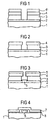
FIG 1: Auf ein Substrat 1 werden eine bspw. aus Nitrid bestehende
Ätzstopschicht 2, eine Siliziumoxid-Schicht 3 und eine
Maskenschicht 4 mit bekannten Verfahren aufgebracht. Die
Dicken der Schichten 2 und 3 können bspw. 20 nm und 50 nm betragen.
Das Substrat kann bereits fertiggestellte Schaltungselemente
enthalten, beispielsweise einen elektrischen
Anschluß für die herzustellende Platinstruktur. Die optionale
Ätzstopschicht besteht vorzugsweise aus Siliziumnitrid. Die
Maskenschicht 4 kann entweder eine Fotolackschicht sein, die
entsprechend der herzustellenden Platinstruktur belichtet und
entwickelt wird, so daß sie im Bereich der herzustellenden
Platinstruktur eine Öffnung aufweist. Sie kann aber auch eine
sog. Hartmaske sein, die bspw. aus Siliziumnitrid besteht,
und die mit Hilfe einer entsprechend strukturierten zusätzlichen
Fotomaske 4' (gestrichelt dargestellt) erzeugt wird. Für
die weiteren Schritte wird dann die Hartmaske 4 nach Entfernung
der Lackmaske 4' als Maske 4 verwendet. Bei dieser Variante
ergibt sich der Vorteil, daß das Platinmetall auch
heiß gesputtert werden kann. Mit der Maske 4 wird die Siliziumoxid-Schicht
3 geätzt. In diesem Ausführungsbeispiel wird
die Oxidschicht 3 zunächst anisotrop bis zur Ätzstopschicht 2
geätzt.1: A substrate 1 is made of nitride, for example
FIG 2: Anschließend erfolgt eine isotrope Ätzung der Siliziumoxid-Schicht
selektiv zur Ätzstopschicht 2, beispielsweise
in einem Naßätzschritt. Dadurch hängt die Maske 4 über
den Rand der Siliziumoxidmaske 3 über, die Gesamtstruktur besitzt
also eine negative Flanke.2: An isotropic etching of the silicon oxide layer then takes place
selective to the
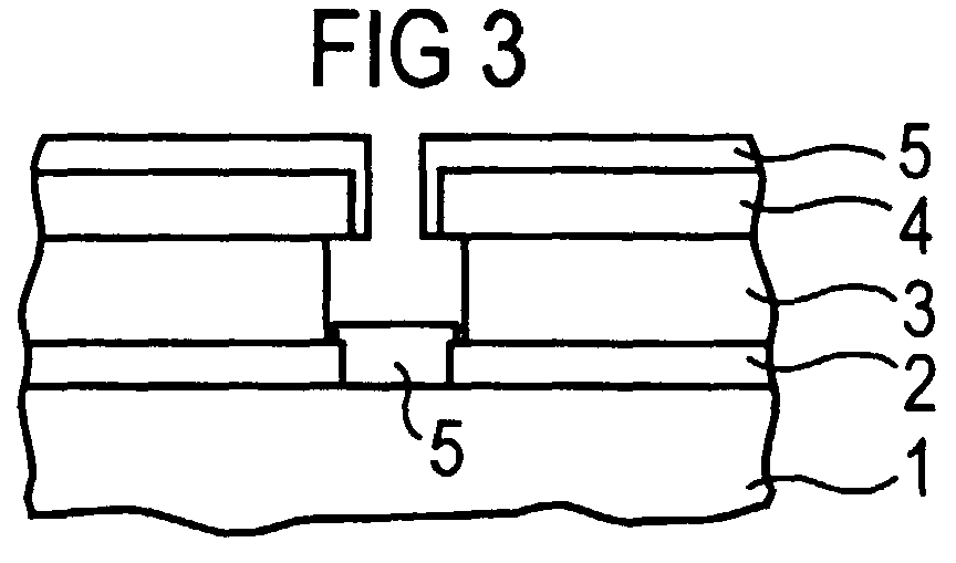
FIG 3: Die freiliegende Ätzstopschicht wird entfernt, so daß
das Substrat - ggf. mit einer Anschlußstruktur für die Platinstruktur
- freiliegt. Auf diese Anordnung wird ganzflächig
ein Platinmetall 5, vorzugsweise Pt aufgebracht, beispielsweise
durch einen Sputterprozeß. Die Flanken der Siliziumoxid-Maske
3 werden dabei nicht beschichtet, so daß im
nachfolgenden Siliziumoxid-Naßätzprozeß das Lösungsmittel an
diesen Stellen angreifen kann und das auf der Maskenoberfläche
aufliegende Platin mit entfernt wird.3: The exposed etch stop layer is removed so that
the substrate - possibly with a connection structure for the platinum structure
- exposed. This arrangement is the whole area
a
FIG 4: Nach Durchführung des Siliziumoxid-Ätzprozesses verbleibt lediglich das die Platinstruktur bildende Platin auf der Substratoberfläche. Ein Speicherkondensator kann durch Aufbringen eines Speicherdielektrikums 6, insbesondere eines hoch-ε-Dielektrikums oder eines Ferroelektrikums wie oben erläutert, und anschließenden Herstellen einer zweiten Kondensatorelektrode 7 (beispielsweise ebenfalls aus Platin) fertiggestellt werden. 4: After the silicon oxide etching process has been carried out, there remains only the platinum forming the platinum structure the substrate surface. A storage capacitor can pass through Application of a storage dielectric 6, in particular one high ε dielectric or a ferroelectric as explained above, and then producing a second capacitor electrode 7 (also made of platinum, for example) become.
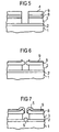
FIG 5: Im zweiten Ausführungsbeispiel wird wie beim ersten
Ausführungsbeispiel zunächst vorzugsweise eine Ätzstopschicht
2 auf das Substrat 1 aufgebracht. Darüber wird eine Doppelschicht
aus Siliziumoxid 3 und Polysilizium 8 abgeschieden.
Anschließend kann eine Oxidationsschutzschicht 9, insbesondere
eine Nitridschicht, abgeschieden werden. Die Schichtenfolge
3, 8, 9 wird dann mit Hilfe einer Fotomaske 4, die an
der Stelle der herzustellenden Platinstruktur eine Öffnung
aufweist, bis zur Ätzstopschicht 2 anisotrop geätzt. Die
Lackmaske 4 kann anschließend entfernt werden.FIG 5: In the second embodiment, as in the first
Embodiment preferably first an
FIG 6: Es wird eine thermische Oxidation durchgeführt, die
das Polysilizium an den freiliegenden Stellen unter Volumenvergrößerung
in Siliziumoxid umwandelt. Dadurch wird die Öffnung
in der Polysiliziumschicht 8 verkleinert und es entsteht
ein Überhang über die Siliziumoxidstruktur. Die Maske für den
Lift-off-Prozeß besteht hier also aus der Siliziumoxidschicht
und der Polysiliziumschicht (sowie ggf. der Nitridschicht).
Die optionale Oxidationsschutzschicht 9 bewirkt einen größeren
Überhang, da dann das Polysilizium 8 nur an den freiliegenden
Kanten oxidieren kann. Bei diesem Ausführungsbeispiel
muß in jedem Fall beim Layout berücksichtigt werden, daß aufgrund
der Oxidation die Öffnung gegenüber der ursprünglichen
Lackmaske 4 verkleinert wird.6: A thermal oxidation is carried out
the polysilicon at the exposed locations with an increase in volume
converted to silicon oxide. This will open up
reduced in size in the
FIG 7: Das weiter Verfahren kann hier im ersten Ausführungsbeispiel
durchgeführt werden, d.h. es wird die Ätzstopschicht
2 entfernt, dann ein Platinmetall aufgebracht und das auf der
Maskenoberfläche aufliegende Platinmetall gemeinsam mit der
Maske entfernt. Wie erläutert, kann anschließend ein Kondensator
fertiggestellt werden.7: The further process can be done here in the first embodiment
be carried out, i.e. it becomes the
Claims (9)
Applications Claiming Priority (2)
| Application Number | Priority Date | Filing Date | Title |
|---|---|---|---|
| DE19717363A DE19717363C2 (en) | 1997-04-24 | 1997-04-24 | Manufacturing process for a platinum metal structure using a lift-off process and use of the manufacturing process |
| DE19717363 | 1997-04-24 |
Publications (2)
| Publication Number | Publication Date |
|---|---|
| EP0892425A2 true EP0892425A2 (en) | 1999-01-20 |
| EP0892425A3 EP0892425A3 (en) | 2000-07-19 |
Family
ID=7827644
Family Applications (1)
| Application Number | Title | Priority Date | Filing Date |
|---|---|---|---|
| EP98105612A Ceased EP0892425A3 (en) | 1997-04-24 | 1998-03-27 | Fabriciation method for a platinum-metal pattern by means of a lift-off process |
Country Status (6)
| Country | Link |
|---|---|
| US (1) | US6051485A (en) |
| EP (1) | EP0892425A3 (en) |
| JP (1) | JPH10303200A (en) |
| KR (1) | KR100470541B1 (en) |
| DE (1) | DE19717363C2 (en) |
| TW (1) | TW423111B (en) |
Cited By (1)
| Publication number | Priority date | Publication date | Assignee | Title |
|---|---|---|---|---|
| WO2001003166A1 (en) * | 1999-06-29 | 2001-01-11 | Infineon Technologies Ag | Method for producing an electrode |
Families Citing this family (11)
| Publication number | Priority date | Publication date | Assignee | Title |
|---|---|---|---|---|
| KR100388683B1 (en) * | 2001-03-06 | 2003-06-25 | 삼성전자주식회사 | Method for manufacturing capacitor in semiconductor device |
| KR100490575B1 (en) * | 2001-08-03 | 2005-05-17 | 야마하 가부시키가이샤 | Method of forming noble metal thin film pattern |
| JP4410685B2 (en) * | 2002-12-19 | 2010-02-03 | インターナショナル・ビジネス・マシーンズ・コーポレーション | Method for forming a fin-type FET |
| US7677696B2 (en) * | 2004-03-31 | 2010-03-16 | Canon Kabushiki Kaisha | Liquid discharge head |
| US7999353B1 (en) * | 2005-04-26 | 2011-08-16 | Northwestern University | Mesoscale pyramids, hole arrays and methods of preparation |
| KR101201972B1 (en) * | 2006-06-30 | 2012-11-15 | 삼성디스플레이 주식회사 | Thin film transistor array substrate and method for fabricating the same |
| KR100807226B1 (en) * | 2006-08-21 | 2008-02-28 | 삼성전자주식회사 | Manufacturing Method of Semiconductor Device |
| JP2010040616A (en) * | 2008-08-01 | 2010-02-18 | Opnext Japan Inc | Method for forming electrode and semiconductor device |
| KR102421575B1 (en) * | 2017-12-01 | 2022-07-18 | 삼성디스플레이 주식회사 | Organic light-emitting apparatus and the method for manufacturing of the organic light-emitting display apparatus |
| KR102812261B1 (en) * | 2018-11-19 | 2025-05-27 | 삼성디스플레이 주식회사 | Method for forming emitting device pattern and display device using the same |
| JP2023523680A (en) | 2020-03-31 | 2023-06-07 | マイクロソフト テクノロジー ライセンシング,エルエルシー | Side-gate type semiconductor-superconductor hybrid device |
Family Cites Families (29)
| Publication number | Priority date | Publication date | Assignee | Title |
|---|---|---|---|---|
| JPS5394767A (en) * | 1977-01-31 | 1978-08-19 | Hitachi Ltd | Manufacture of semiconductor device |
| JPS55154737A (en) * | 1979-05-22 | 1980-12-02 | Chiyou Lsi Gijutsu Kenkyu Kumiai | Method of forming pattern |
| US4283483A (en) * | 1979-07-19 | 1981-08-11 | Hughes Aircraft Company | Process for forming semiconductor devices using electron-sensitive resist patterns with controlled line profiles |
| JPS5811512B2 (en) * | 1979-07-25 | 1983-03-03 | 超エル・エス・アイ技術研究組合 | Pattern formation method |
| JPS57183037A (en) * | 1981-05-06 | 1982-11-11 | Nec Corp | Formation of pattern |
| JPS5891640A (en) * | 1981-11-26 | 1983-05-31 | Toshiba Corp | Manufacture of semiconductor device |
| US4428796A (en) * | 1982-08-02 | 1984-01-31 | Fairchild Camera And Instrument Corporation | Adhesion bond-breaking of lift-off regions on semiconductor structures |
| US4497684A (en) * | 1983-02-22 | 1985-02-05 | Amdahl Corporation | Lift-off process for depositing metal on a substrate |
| US4533624A (en) * | 1983-05-23 | 1985-08-06 | Sperry Corporation | Method of forming a low temperature multilayer photoresist lift-off pattern |
| JPS62120046A (en) * | 1985-11-20 | 1987-06-01 | Sanyo Electric Co Ltd | Manufacture of semiconductor device |
| IT1190294B (en) * | 1986-02-13 | 1988-02-16 | Selenia Ind Elettroniche | A MULTI-LAYER PHOTOPOLYMER (MLR) STRUCTURE FOR THE MANUFACTURE OF MESFET DEVICES WITH SUBMICROMETRIC GATES AND WITH RECESSED CHANNEL (RECESS) OF VARIABLE LENGTH |
| JPS6315417A (en) * | 1986-07-08 | 1988-01-22 | Fujitsu Ltd | Manufacture of semiconductor device |
| JPS63175480A (en) * | 1987-01-14 | 1988-07-19 | Nec Corp | Manufacture of recessed mesfet |
| JPH01161787A (en) * | 1987-12-18 | 1989-06-26 | Toshiba Corp | Method for processing oxide superconducting film |
| JPH0269936A (en) * | 1988-07-28 | 1990-03-08 | Siemens Ag | Method of making resin structure on semiconductor material |
| US5024896A (en) * | 1989-07-06 | 1991-06-18 | International Business Machines Corporation | Collimated metal deposition |
| US5053348A (en) * | 1989-12-01 | 1991-10-01 | Hughes Aircraft Company | Fabrication of self-aligned, t-gate hemt |
| JPH04171809A (en) * | 1990-11-05 | 1992-06-19 | Nec Corp | Manufacture of semiconductor device |
| JP2740050B2 (en) * | 1991-03-19 | 1998-04-15 | 株式会社東芝 | Groove embedded wiring formation method |
| KR920020676A (en) * | 1991-04-09 | 1992-11-21 | 김광호 | Device Separation Method of Semiconductor Device |
| US5240878A (en) * | 1991-04-26 | 1993-08-31 | International Business Machines Corporation | Method for forming patterned films on a substrate |
| US5155053A (en) * | 1991-05-28 | 1992-10-13 | Hughes Aircraft Company | Method of forming t-gate structure on microelectronic device substrate |
| US5242534A (en) * | 1992-09-18 | 1993-09-07 | Radiant Technologies | Platinum lift-off process |
| JP3102965B2 (en) * | 1993-03-12 | 2000-10-23 | 三菱電機株式会社 | Distance measuring device |
| JPH06295856A (en) * | 1993-04-09 | 1994-10-21 | Sumitomo Heavy Ind Ltd | He pressure control method and pressure controller for aligner |
| JPH0837233A (en) * | 1994-07-22 | 1996-02-06 | Rohm Co Ltd | Manufacture of semiconductor device |
| US5554488A (en) * | 1994-07-28 | 1996-09-10 | Northern Telecom Limited | Semiconductor device structure and method of formation thereof |
| JPH08298263A (en) * | 1995-04-27 | 1996-11-12 | Nec Corp | Manufacture of semiconductor device |
| US5705432A (en) * | 1995-12-01 | 1998-01-06 | Hughes Aircraft Company | Process for providing clean lift-off of sputtered thin film layers |
-
1997
- 1997-04-24 DE DE19717363A patent/DE19717363C2/en not_active Expired - Fee Related
-
1998
- 1998-03-27 EP EP98105612A patent/EP0892425A3/en not_active Ceased
- 1998-04-08 TW TW087105257A patent/TW423111B/en not_active IP Right Cessation
- 1998-04-21 JP JP10128210A patent/JPH10303200A/en active Pending
- 1998-04-22 KR KR10-1998-0014293A patent/KR100470541B1/en not_active Expired - Fee Related
- 1998-04-24 US US09/066,245 patent/US6051485A/en not_active Expired - Lifetime
Cited By (1)
| Publication number | Priority date | Publication date | Assignee | Title |
|---|---|---|---|---|
| WO2001003166A1 (en) * | 1999-06-29 | 2001-01-11 | Infineon Technologies Ag | Method for producing an electrode |
Also Published As
| Publication number | Publication date |
|---|---|
| JPH10303200A (en) | 1998-11-13 |
| US6051485A (en) | 2000-04-18 |
| KR100470541B1 (en) | 2005-03-16 |
| DE19717363A1 (en) | 1998-10-29 |
| TW423111B (en) | 2001-02-21 |
| DE19717363C2 (en) | 2001-09-06 |
| EP0892425A3 (en) | 2000-07-19 |
| KR19980081598A (en) | 1998-11-25 |
Similar Documents
| Publication | Publication Date | Title |
|---|---|---|
| DE19638684C2 (en) | Semiconductor device with a contact hole | |
| DE4142469B4 (en) | Process for the production and removal of temporary silicon dioxide structures | |
| DE4201506C2 (en) | Method for producing DRAM memory cells with stacked capacitors with fin structure | |
| WO2001043171A1 (en) | Method for producing a hard mask | |
| DE2723944A1 (en) | ARRANGEMENT OF A STRUCTURED LAYER AND A PATTERN OF DEFINED THICKNESS AND METHOD OF MANUFACTURING IT | |
| EP0892425A2 (en) | Fabriciation method for a platinum-metal pattern by means of a lift-off process | |
| DE60133740T2 (en) | MANUFACTURING METHOD OF AN INTEGRATED CIRCUIT STRUCTURE WITH GUIDING LAYERS WITH LARGE INTERIOR SURFACES | |
| DE3402825A1 (en) | SEMICONDUCTOR ARRANGEMENT WITH INSULATION GROOVE AND PRODUCTION METHOD | |
| DE602004008429T2 (en) | MAGNETIC TUNNEL TRANSFER STACKING IN TWO STEPS | |
| DE10012198B4 (en) | Cylindrical capacitor device with HSG silicon on the inside and process for its production | |
| EP0895278A2 (en) | Patterning process | |
| DE19852256B4 (en) | Process for etching platinum | |
| WO2000034985A2 (en) | Method for structuring a metalliferous layer | |
| DE68922085T2 (en) | Semiconductor device and method for manufacturing a semiconductor device. | |
| DE19620185C2 (en) | Method of manufacturing a capacitor of a semiconductor device | |
| EP0867926A1 (en) | Capacitor electrode made of platinum metal | |
| DE10312469A1 (en) | Method of manufacturing a semiconductor structure | |
| DE10031881A1 (en) | Semiconductor device for e.g. high speed RAM, has titanium oxide film formed uniformly on lower strontium-ruthenium oxide film formed on semiconductor substrate | |
| DE10262115B4 (en) | Integrated circuit device with a plurality of stacked capacitors, metal-insulator-metal capacitor and manufacturing method thereof | |
| EP1277230B1 (en) | Method for producing capacitor structures | |
| EP0902461A2 (en) | Process for forming structures with high aspect ratio | |
| DE19710491C2 (en) | Manufacturing method for semiconductor memory device | |
| EP0931342B1 (en) | A barrier-free semiconductor storage assembly and process for its production | |
| DE4200284C2 (en) | Semiconductor device and method for its production | |
| DE112006000261B4 (en) | Method for producing a capacitive element by means of etching |
Legal Events
| Date | Code | Title | Description |
|---|---|---|---|
| PUAI | Public reference made under article 153(3) epc to a published international application that has entered the european phase |
Free format text: ORIGINAL CODE: 0009012 |
|
| AK | Designated contracting states |
Kind code of ref document: A2 Designated state(s): DE FR GB IE IT |
|
| AX | Request for extension of the european patent |
Free format text: AL;LT;LV;MK;RO;SI |
|
| PUAL | Search report despatched |
Free format text: ORIGINAL CODE: 0009013 |
|
| AK | Designated contracting states |
Kind code of ref document: A3 Designated state(s): AT BE CH DE DK ES FI FR GB GR IE IT LI LU MC NL PT SE |
|
| AX | Request for extension of the european patent |
Free format text: AL;LT;LV;MK;RO;SI |
|
| 17P | Request for examination filed |
Effective date: 20000818 |
|
| AKX | Designation fees paid |
Free format text: DE FR GB IE IT |
|
| RAP1 | Party data changed (applicant data changed or rights of an application transferred) |
Owner name: INFINEON TECHNOLOGIES AG |
|
| 17Q | First examination report despatched |
Effective date: 20041217 |
|
| STAA | Information on the status of an ep patent application or granted ep patent |
Free format text: STATUS: THE APPLICATION HAS BEEN REFUSED |
|
| 18R | Application refused |
Effective date: 20050723 |