EP0902461A2 - Process for forming structures with high aspect ratio - Google Patents
Process for forming structures with high aspect ratio Download PDFInfo
- Publication number
- EP0902461A2 EP0902461A2 EP98114572A EP98114572A EP0902461A2 EP 0902461 A2 EP0902461 A2 EP 0902461A2 EP 98114572 A EP98114572 A EP 98114572A EP 98114572 A EP98114572 A EP 98114572A EP 0902461 A2 EP0902461 A2 EP 0902461A2
- Authority
- EP
- European Patent Office
- Prior art keywords
- layer
- aspect ratio
- mask
- high aspect
- etching
- Prior art date
- Legal status (The legal status is an assumption and is not a legal conclusion. Google has not performed a legal analysis and makes no representation as to the accuracy of the status listed.)
- Withdrawn
Links
Images


Classifications
-
- C—CHEMISTRY; METALLURGY
- C23—COATING METALLIC MATERIAL; COATING MATERIAL WITH METALLIC MATERIAL; CHEMICAL SURFACE TREATMENT; DIFFUSION TREATMENT OF METALLIC MATERIAL; COATING BY VACUUM EVAPORATION, BY SPUTTERING, BY ION IMPLANTATION OR BY CHEMICAL VAPOUR DEPOSITION, IN GENERAL; INHIBITING CORROSION OF METALLIC MATERIAL OR INCRUSTATION IN GENERAL
- C23F—NON-MECHANICAL REMOVAL OF METALLIC MATERIAL FROM SURFACE; INHIBITING CORROSION OF METALLIC MATERIAL OR INCRUSTATION IN GENERAL; MULTI-STEP PROCESSES FOR SURFACE TREATMENT OF METALLIC MATERIAL INVOLVING AT LEAST ONE PROCESS PROVIDED FOR IN CLASS C23 AND AT LEAST ONE PROCESS COVERED BY SUBCLASS C21D OR C22F OR CLASS C25
- C23F4/00—Processes for removing metallic material from surfaces, not provided for in group C23F1/00 or C23F3/00
-
- H—ELECTRICITY
- H10—SEMICONDUCTOR DEVICES; ELECTRIC SOLID-STATE DEVICES NOT OTHERWISE PROVIDED FOR
- H10B—ELECTRONIC MEMORY DEVICES
- H10B12/00—Dynamic random access memory [DRAM] devices
- H10B12/01—Manufacture or treatment
- H10B12/02—Manufacture or treatment for one transistor one-capacitor [1T-1C] memory cells
- H10B12/03—Making the capacitor or connections thereto
- H10B12/033—Making the capacitor or connections thereto the capacitor extending over the transistor
-
- H—ELECTRICITY
- H10—SEMICONDUCTOR DEVICES; ELECTRIC SOLID-STATE DEVICES NOT OTHERWISE PROVIDED FOR
- H10D—INORGANIC ELECTRIC SEMICONDUCTOR DEVICES
- H10D1/00—Resistors, capacitors or inductors
- H10D1/01—Manufacture or treatment
- H10D1/041—Manufacture or treatment of capacitors having no potential barriers
- H10D1/042—Manufacture or treatment of capacitors having no potential barriers using deposition processes to form electrode extensions
-
- H—ELECTRICITY
- H10—SEMICONDUCTOR DEVICES; ELECTRIC SOLID-STATE DEVICES NOT OTHERWISE PROVIDED FOR
- H10D—INORGANIC ELECTRIC SEMICONDUCTOR DEVICES
- H10D1/00—Resistors, capacitors or inductors
- H10D1/60—Capacitors
- H10D1/68—Capacitors having no potential barriers
- H10D1/682—Capacitors having no potential barriers having dielectrics comprising perovskite structures
-
- H—ELECTRICITY
- H10—SEMICONDUCTOR DEVICES; ELECTRIC SOLID-STATE DEVICES NOT OTHERWISE PROVIDED FOR
- H10D—INORGANIC ELECTRIC SEMICONDUCTOR DEVICES
- H10D1/00—Resistors, capacitors or inductors
- H10D1/60—Capacitors
- H10D1/68—Capacitors having no potential barriers
- H10D1/692—Electrodes
- H10D1/711—Electrodes having non-planar surfaces, e.g. formed by texturisation
- H10D1/716—Electrodes having non-planar surfaces, e.g. formed by texturisation having vertical extensions
-
- H—ELECTRICITY
- H10—SEMICONDUCTOR DEVICES; ELECTRIC SOLID-STATE DEVICES NOT OTHERWISE PROVIDED FOR
- H10P—GENERIC PROCESSES OR APPARATUS FOR THE MANUFACTURE OR TREATMENT OF DEVICES COVERED BY CLASS H10
- H10P14/00—Formation of materials, e.g. in the shape of layers or pillars
- H10P14/60—Formation of materials, e.g. in the shape of layers or pillars of insulating materials
- H10P14/69—Inorganic materials
- H10P14/692—Inorganic materials composed of oxides, glassy oxides or oxide-based glasses
- H10P14/6938—Inorganic materials composed of oxides, glassy oxides or oxide-based glasses the material containing at least one metal element, e.g. metal oxides, metal oxynitrides or metal oxycarbides
- H10P14/69398—Inorganic materials composed of oxides, glassy oxides or oxide-based glasses the material containing at least one metal element, e.g. metal oxides, metal oxynitrides or metal oxycarbides the material having a perovskite structure, e.g. BaTiO3
-
- H—ELECTRICITY
- H10—SEMICONDUCTOR DEVICES; ELECTRIC SOLID-STATE DEVICES NOT OTHERWISE PROVIDED FOR
- H10P—GENERIC PROCESSES OR APPARATUS FOR THE MANUFACTURE OR TREATMENT OF DEVICES COVERED BY CLASS H10
- H10P50/00—Etching of wafers, substrates or parts of devices
- H10P50/71—Etching of wafers, substrates or parts of devices using masks for conductive or resistive materials
-
- H—ELECTRICITY
- H10—SEMICONDUCTOR DEVICES; ELECTRIC SOLID-STATE DEVICES NOT OTHERWISE PROVIDED FOR
- H10P—GENERIC PROCESSES OR APPARATUS FOR THE MANUFACTURE OR TREATMENT OF DEVICES COVERED BY CLASS H10
- H10P76/00—Manufacture or treatment of masks on semiconductor bodies, e.g. by lithography or photolithography
- H10P76/40—Manufacture or treatment of masks on semiconductor bodies, e.g. by lithography or photolithography of masks comprising inorganic materials
- H10P76/408—Manufacture or treatment of masks on semiconductor bodies, e.g. by lithography or photolithography of masks comprising inorganic materials characterised by their sizes, orientations, dispositions, behaviours or shapes
- H10P76/4083—Manufacture or treatment of masks on semiconductor bodies, e.g. by lithography or photolithography of masks comprising inorganic materials characterised by their sizes, orientations, dispositions, behaviours or shapes characterised by their behaviours during the lithography processes, e.g. soluble masks or redeposited masks
Definitions
- the present invention relates to a production method of structures with a high aspect ratio as well Structures with a high aspect ratio.
- the basic design of a elementary memory cell as well as the structure of the memory cell The materials used have, however, essentially not changed.
- the capacitor of the memory cell has Doped silicon or polysilicon electrodes and one dielectric layer arranged between the electrodes Silicon dioxide and / or silicon nitride.
- the capacitance of the capacitor should have a value of at least about 30 fF.
- the lateral expansion of the capacitor had to and must be continuously reduced in order to be able to achieve the aforementioned increase in storage density.
- Another way to ensure sufficient capacitance of the capacitor is to use other materials between the capacitor electrodes.
- new materials in particular paraelectrics and ferroelectrics, have been used between the capacitor electrodes of a memory cell.
- These new materials have a significantly higher relative dielectric constant (> 20) than the conventional silicon oxide / silicon nitride ( ⁇ 8). Therefore, by using these materials, with the same capacity and the same lateral extent of the memory cell, the required capacitor area and thus the required complexity of the structuring of the capacitor can be significantly reduced.
- barium strontium titanate BST, (Ba, Sr) TiO 3
- lead zirconate titanate PZT, Pb (Zr, Ti) O 3
- lanthanum-doped lead zirconate titanate or strontium bismuth tantalate SBT, SrBi 2 Ta 2 O 9
- the method according to the invention allows very high ( ⁇ 1 ⁇ m) and very thin ( ⁇ 50 nm) structures in very few Process steps and relatively simple with just one mask technique and generate quickly. Structures with such large aspect ratios, especially if they are made of a conductive material can not exist otherwise or only with great effort be generated.
- a plasma etching method is preferred for dry etching of the layer used. It is further preferred if during the Dry etching of the layer, a gas or gas mixture, is preferred a noble gas is provided, which with the material to be generated Structure does not form volatile compounds.
- a number of methods can be used to dry etch the layer be used.
- RIE reactive ion etching
- MIE magnetic field-assisted reactive ion etching
- ECR Electron Cyclotron Resonance
- ICP inductively coupled plasma etching
- the aspect ratio of Structure greater than 2, preferably greater than 10, in particular is greater than 20.
- the structure is preferred as self-stabilizing Structure trained.
- the Structure is preferred if the Structure as a self-contained structure, for example is designed as a closed ring.
- the method according to the invention can be used with a large number of Materials are carried out.
- a metal especially copper, iron, cobalt, Nickel, or a 4d or 5d transition metal, in particular a platinum metal.
- this further layer is a Insulation layer.
- the further layer is a ferroelectric Material, a dielectric material, in particular a dielectric material with a high relative dielectric constant, a perovskite or precursors of these materials contains. It is said to be under a preliminary stage of the above Materials are understood to be a material that is made by a suitable heat treatment (e.g. tempering), if necessary with the addition of oxygen, in the materials mentioned can be converted.
- a suitable heat treatment e.g. tempering
- strontium bismuth tantalate SBT, SrBi 2 Ta 2 O 9
- lead zirconate titanate PZT, Pb (Zr, Ti) O 3
- lead lanthanum titanate PLA
- Pb, La lead lanthanum zirconate titanate
- PZT lead lanthanum zirconate titanate
- Pb , La Zr, Ti
- the material to be produced Structure in the form of a layer on a conductive Layer is applied.
- two form closed rings over the conductive layer are electrically connected together. This is also supposed to include the case that only a relatively thick, conductive Layer is created, the material of the upper part of the Layer for generating the speech positions and the material of the lower part of the layer for the conductive connection of the speech positions serves.
- Figures 1 to 4 show a schematic representation of a Method according to the invention for generating structures with a high aspect ratio.
- a platinum layer 3 is deposited on this barrier layer 2 by a CVD or sputtering process. The platinum of the platinum layer 3 forms the material of the structure to be produced with a high aspect ratio.
- a layer of lacquer is then applied. This lacquer layer is exposed and developed so that the lacquer mask 5 is formed.
- a so-called Hard mask for example a SiO 2 hard mask "can be used. The resulting structure is shown in FIG. 1.
- the platinum layer is made using the resist mask 5 3 dry etched.
- the structuring of the platinum layer 3 is done by a so-called plasma-assisted anisotropic etching process. Gas mixtures are used that with the platinum of the platinum layer no volatile compounds form. In the present case, a pure argon gas was used used.
- the gas is excited in an alternating electromagnetic field at low pressures.
- 5 shows the principle of operation of the parallel plate reactor 20 used.
- the argon gas is fed to the actual reactor chamber 22 via the gas inlet 21 and pumped out again through the gas outlet 29.
- the lower plate 24 of the parallel plate reactor is connected to a high-frequency source 28 via a capacitance 27 and serves as a substrate holder.
- the gas is converted into a plasma 25. Since the mobility of the electrons is greater than that of the gas cations, the upper and lower plates 23, 24 charge negatively with respect to the plasma 25.
- both plates 23, 24 exert a high attraction on the positively charged gas cations, so that they are exposed to permanent bombardment by these Ar + ions. Since the gas pressure is also kept low, typically 0.1-10 Pa, there is only a slight scattering of the ions among one another and on the neutral particles, and the ions strike the surface of the platinum layer 3, which passes over the substrate 1 (not shown), almost perpendicularly. is held on the lower plate 24 of the parallel plate reactor. This allows the mask 5 (not shown) to be imaged well on the underlying platinum layer 3 to be etched.
- the barrier layer 2 is then structured by a further anisotropic dry etching and the resist mask 5 is removed by an ashing step.
- a paint mask SiO 2 hard mask "is used this mask can be further etched, a so-called HF-Dip ", are removed.
- the redepositions 6 are retained.
- structures 6 have been created which have a high aspect ratio (see FIG. 3). It should be noted that FIG. 3 shows a section through an annular ring represents closed speech position 6. Due to the ring-shaped closed shape, speech position 6, even with a very large ratio of height to width, can stabilize itself mechanically.
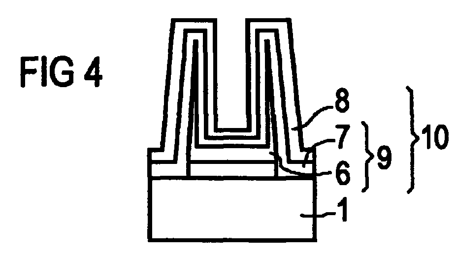
- a barium strontium titanate layer 7 (BST, (Ba, Sr) TiO 3 ) is applied to the redepositions 6 as conformingly as possible by means of a CVD process.
- the redepositions 6 and the BST layer 7 thus in turn form a structure 9 which has a high aspect ratio.
- a conductive layer 8 is subsequently applied to the BST layer 7. This can also be done in a compliant manner, so that a third structure 10 is formed, which also has a high aspect ratio.
- the resulting overall structure is shown in FIG. 4.
- the structure 10 resulting from the method according to the invention can now be called a so-called Crown capacitor "can be used in the memory cell of a DRAM memory chip. Due to the crown structure, such a capacitor has a much larger area than a simple planar capacitor. Accordingly, the capacitance of the Crown capacitor ".
Landscapes
- Engineering & Computer Science (AREA)
- Chemical & Material Sciences (AREA)
- Manufacturing & Machinery (AREA)
- Materials Engineering (AREA)
- Mechanical Engineering (AREA)
- Metallurgy (AREA)
- Organic Chemistry (AREA)
- Semiconductor Memories (AREA)
- Drying Of Semiconductors (AREA)
- Manufacturing Of Electric Cables (AREA)
- Shielding Devices Or Components To Electric Or Magnetic Fields (AREA)
Abstract
Erfindungsgemäß wird ein zur Erzeugung von Strukturen mit einem hohen Aspektverhältnis bereitgestellt, das die folgenden Schritte aufweist: das Material der zu erzeugenden Struktur wird in Form einer Schicht bereitgestellt, auf die Schicht wird eine Maske aufgebracht, die Schicht wird unter Verwendung der Maske trockengeätzt, so daß Redepositionen des Schichtmaterials an den Seitenwänden der Maske gebildet werden, die Maske wird entfernt, so daß eine Struktur mit einem hohen Aspektverhältnis zurückbleibt.According to the invention, one is used to generate structures with a high aspect ratio provided the following Steps comprises: the material of the structure to be created is provided in the form of a layer, on top of the layer a mask is applied, the layer is used the mask is etched dry, so that the speeches of the Layer material are formed on the side walls of the mask, the mask is removed so that a structure with a remains high aspect ratio.
Durch das erfindungsgemäße Verfahren lassen sich sehr hohe (≥
1 µm) und sehr dünne (≤ 50 nm) Strukturen in nur sehr wenigen
Prozeßschritten und mit nur einer Maskentechnik relativ einfach
und schnell erzeugen. Strukturen mit so großen Aspektverhältnissen,
insbesondere wenn sie aus einem leitenden Material
bestehen, können anders nicht oder nur mit hohem Aufwand
erzeugt werden.
Description
Die vorliegende Erfindung betrifft ein Verfahren zur Erzeugung von Strukturen mit einem hohen Aspektverhältnis sowie Strukturen mit einem hohen Aspektverhältnis.The present invention relates to a production method of structures with a high aspect ratio as well Structures with a high aspect ratio.
Während der letzten 25 Jahre hat sich die Speicherdichte von
DRAM-Speicherbausteinen von einer Generation zur nächsten Generation
jeweils vervierfacht. Das prinzipielle Design einer
elementaren Speicherzelle sowie die zum Aufbau der Speicherzelle
verwendeten Materialien haben sich dabei jedoch im wesentlichen
nicht verändert. Eine DRAM-Speicherzelle besteht
wie vor 25 Jahren aus einem Transistor und einem Kondensator,
der die zur Darstellung der Information notwendige Ladung
speichert. Der Kondensator der Speicherzelle besitzt dabei
Elektroden aus dotiertem Silizium bzw. Polysilizium und eine
zwischen den Elektroden angeordnete dielektrische Schicht aus
Siliziumdioxid und/oder Siliziumnitrid.Over the past 25 years, the storage density of
DRAM memory chips from one generation to the next generation
each quadrupled. The basic design of a
elementary memory cell as well as the structure of the memory cell
The materials used have, however, essentially
not changed. There is a DRAM memory cell
like a transistor and a
Um die in einem Kondensator gespeicherte Ladung reproduzierbar
auslesen zu können, sollte die Kapazität des Kondensators
mindestens einen Wert von etwa 30 fF besitzen. Gleichzeitig
mußte und muß die laterale Ausdehnung des Kondensators ständig
verkleinert werden, um die genannte Erhöhung der Speicherdichte
erzielen zu können. Diese an sich gegenläufigen
Anforderungen an den Kondensator der Speicherzelle führten
und führen zu einer immer komplexeren Strukturierung des Kondensators
(![]()
![]()
Ein weiterer Weg, eine ausreichende Kapazität des Kondensators zu gewährleisten, liegt in der Verwendung anderer Materialien zwischen den Kondensatorelektroden. In letzter Zeit werden daher anstatt des herkömmlichen Siliziumoxids/ Siliziumnitrids neue Materialien, insbesondere Paraelektrika und Ferroelektrika, zwischen den Kondensatorelektroden einer Speicherzelle verwendet. Diese neuen Materialien besitzen eine deutlich höhere relative Dielektrizitätskonstante (> 20) als das herkömmliche Siliziumoxid/Siliziumnitrid (< 8). Daher kann durch den Einsatz dieser Materialien, bei gleicher Kapazität und gleicher lateralen Ausdehnung der Speicherzelle, die benötigte Kondensatorfläche und damit die benötigte Komplexität der Strukturierung des Kondensators deutlich vermindert werden. Beispielsweise kommen Bariumstrontiumtitanat (BST, (Ba,Sr)TiO3), Bleizirkonattitanat (PZT, Pb(Zr,Ti)O3) bzw. Lanthan-dotiertes Bleizirkonattitanat oder Strontiumwismuttantalat (SBT, SrBi2Ta2O9) zum Einsatz.Another way to ensure sufficient capacitance of the capacitor is to use other materials between the capacitor electrodes. Recently, instead of the conventional silicon oxide / silicon nitride, new materials, in particular paraelectrics and ferroelectrics, have been used between the capacitor electrodes of a memory cell. These new materials have a significantly higher relative dielectric constant (> 20) than the conventional silicon oxide / silicon nitride (<8). Therefore, by using these materials, with the same capacity and the same lateral extent of the memory cell, the required capacitor area and thus the required complexity of the structuring of the capacitor can be significantly reduced. For example, barium strontium titanate (BST, (Ba, Sr) TiO 3 ), lead zirconate titanate (PZT, Pb (Zr, Ti) O 3 ) or lanthanum-doped lead zirconate titanate or strontium bismuth tantalate (SBT, SrBi 2 Ta 2 O 9 ) are used.
Leider bedingt die Verwendung der neuen Paraelektrika bzw. Ferroelektrika auch die Verwendung neuer Elektrodenmaterialien. Die neuen Paraelektrika bzw. Ferroelektrika werden üblicherweise auf bereits vorhandenen Elektroden (Bodenelektroden) abgeschieden. Die Prozessierung erfolgt unter hohen Temperaturen, bei denen die Materialien, aus denen normalerweise die Kondensatorelektroden bestehen, so z.B. dotiertes Polysilizium, leicht oxidiert werden und ihre elektrisch leitenden Eigenschaften verlieren, was zum Ausfall der Speicherzelle führen würde.Unfortunately, the use of the new paraelectrics or Ferroelectrics also use new electrode materials. The new paraelectrics and ferroelectrics are common on existing electrodes (Bottom electrodes) deposited. Processing takes place under high temperatures at which the materials from which normally the capacitor electrodes are made, e.g. endowed Polysilicon, easily oxidized and its electrical lose conductive properties, resulting in the failure of the Memory cell would lead.
Wegen ihrer guten Oxidationsbeständigkeit und/oder der Ausbildung elektrisch leitfähiger Oxide gelten 4d und 5d Übergangsmetalle, insbesondere Platinmetalle (Ru, Rh, Pd, Os, Ir, Pt) und insbesondere Platin selbst, sowie Rhenium als aussichtsreiche Kandidaten, die dotiertes Silizium/Polysilizium als Elektrodenmaterial ersetzen könnten. Because of their good oxidation resistance and / or training electrically conductive oxides apply 4d and 5d transition metals, especially platinum metals (Ru, Rh, Pd, Os, Ir, Pt) and especially platinum itself, as well as rhenium as promising Candidates who use doped silicon / polysilicon could replace as electrode material.
Reicht beim ersten Einsatz der neuen Materialien (z.B. Platin
und BST) noch ein einfach strukturierter
Es ist daher die Aufgabe der vorliegenden Erfindung, ein Verfahren zur Erzeugung von Strukturen mit einem hohen Aspektverhältnis, insbesondere aus den genannten Materialien, sowie eine Struktur einem hohen Aspektverhältnis bereitzustellen.It is therefore the object of the present invention, a method to create structures with a high aspect ratio, in particular from the materials mentioned, and to provide a high aspect ratio structure.
Diese Aufgabe wird von dem Verfahren zur Erzeugung von Strukturen mit einem hohen Aspektverhältnis gemäß Patentanspruch 1 sowie der Struktur mit einem hohen Aspektverhältnis gemäß Patentanspruch 15 gelöst. Weitere vorteilhafte Ausführungsformen, Ausgestaltungen und Aspekte der vorliegenden Erfindung ergeben sich aus den Unteransprüchen der Beschreibung und den beiliegenden Zeichnungen.This task is performed by the process of creating structures with a high aspect ratio according to claim 1 and the structure with a high aspect ratio according to claim 15 solved. Further advantageous embodiments, Refinements and aspects of the present invention result from the subclaims of the description and the enclosed drawings.
Erfindungsgemäß wird ein Verfahren zur Erzeugung von Strukturen
mit einem hohen Aspektverhältnis bereitgestellt, das die
folgenden Schritte aufweist:
Durch das erfindungsgemäße Verfahren lassen sich sehr hohe (≥ 1 µm) und sehr dünne (≤ 50 nm) Strukturen in nur sehr wenigen Prozeßschritten und mit nur einer Maskentechnik relativ einfach und schnell erzeugen. Strukturen mit so großen Aspektverhältnissen, insbesondere wenn sie aus einem leitenden Material bestehen, können anders nicht oder nur mit hohem Aufwand erzeugt werden.The method according to the invention allows very high (≥ 1 µm) and very thin (≤ 50 nm) structures in very few Process steps and relatively simple with just one mask technique and generate quickly. Structures with such large aspect ratios, especially if they are made of a conductive material can not exist otherwise or only with great effort be generated.
Bevorzugt wird zum Trockenätzen der Schicht ein Plasmaätzverfahren verwendet. Weiterhin ist bevorzugt, wenn während der Trockenätzung der Schicht ein Gas oder Gasgemisch, bevorzugt ein Edelgas, vorgesehen ist, das mit dem Material der zu erzeugenden Struktur keine flüchtigen Verbindungen bildet.A plasma etching method is preferred for dry etching of the layer used. It is further preferred if during the Dry etching of the layer, a gas or gas mixture, is preferred a noble gas is provided, which with the material to be generated Structure does not form volatile compounds.
Zur Trockenätzung der Schicht können eine Reihe von Vefahren verwendet werden. Bevorzugt werden zur Trockenätzung der Schicht eine reaktive Ionenätzung (RIE, Reactive Ion Etching), eine magnetfeldunterstützte reaktive Ionenätzung (MERIE, Magnetically Enhanced RIE), eine ECR-Ätzung (ECR, Electron Cyclotron Resonance) oder induktiv gekoppelte Plasmaätzverfahren (ICP, TCP) eingesetzt.A number of methods can be used to dry etch the layer be used. Are preferred for dry etching Layer a reactive ion etching (RIE, Reactive Ion Etching), a magnetic field-assisted reactive ion etching (MERIE, Magnetically Enhanced RIE), an ECR etching (ECR, Electron Cyclotron Resonance) or inductively coupled plasma etching (ICP, TCP) used.
Weiterhin ist es vorteilhaft, wenn das Aspektverhältnis der Struktur größer als 2, bevorzugt größer als 10, insbesondere größer als 20, ist. It is also advantageous if the aspect ratio of Structure greater than 2, preferably greater than 10, in particular is greater than 20.
Bevorzugt ist die Struktur als sich selbst stabilisierende Struktur ausgebildet. Insbesondere ist es bevorzugt, wenn die Struktur als in sich geschlossene Struktur, beispielsweise als geschlossener Ring, ausgebildet ist.The structure is preferred as self-stabilizing Structure trained. In particular, it is preferred if the Structure as a self-contained structure, for example is designed as a closed ring.
Das erfindungsgemäße Verfahren kann mit einer Vielzahl von Materialien durchgeführt werden. Bevorzugt enthält die Schicht jedoch ein Metall, insbesondere Kupfer, Eisen, Kobalt, Nickel, oder ein 4d oder 5d Übergangsmetall, insbesondere ein Platinmetall. Weiterhin ist es bevorzugt, wenn die Schicht Platin, Gold, Silber, Iridium, Palladium, Ruthenium, Rhenium oder deren Oxide enthält.The method according to the invention can be used with a large number of Materials are carried out. Preferably contains the However, layer a metal, especially copper, iron, cobalt, Nickel, or a 4d or 5d transition metal, in particular a platinum metal. It is further preferred if the Layer of platinum, gold, silver, iridium, palladium, ruthenium, Contains rhenium or its oxides.
Darüber hinaus ist es bevorzugt, wenn auf die Struktur zumindest eine weitere Schicht so aufgebracht wird, daß wiederum eine Struktur mit einem hohem Aspektverhältnis entsteht. Insbesondere ist es bevorzugt, wenn diese weitere Schicht eine Isolationsschicht ist.In addition, it is preferred if at least on the structure another layer is applied so that again a structure with a high aspect ratio is created. Especially it is preferred if this further layer is a Insulation layer.
Weiterhin ist es bevorzugt, wenn die weitere Schicht ein ferroelektrisches Material, ein dielektrisches Material, insbesondere ein dielektrisches Material hoher relativer Dielektrizitätskonstante, einen Perowskit oder Vorstufen dieser Materialien enthält. Dabei soll unter einer Vorstufe der genannten Materialien ein Material verstanden werden, das durch eine geeignete Wärmebehandlung (z.B. Tempern), gegebenenfalls unter Zuführung von Sauerstoff, in die genannten Materialien umgewandelt werden kann.It is further preferred if the further layer is a ferroelectric Material, a dielectric material, in particular a dielectric material with a high relative dielectric constant, a perovskite or precursors of these materials contains. It is said to be under a preliminary stage of the above Materials are understood to be a material that is made by a suitable heat treatment (e.g. tempering), if necessary with the addition of oxygen, in the materials mentioned can be converted.
So ist es bevorzugt, wenn die weitere Schicht Strontiumwismuttantalat (SBT, SrBi2Ta2O9), Strontiumwismutniobattantalat (SBNT, SrBi2Ta2-xNbxO9, x=0-2) oder Derivate, Bleizirkonattitanat (PZT, Pb(Zr,Ti)O3) oder Derivate oder Bariumstrontiumtitanat (BST, BaxSr1-xTiO3, x=0-1), Bleilanthantitanat (PLT, (Pb, La)TiO3), Bleilanthanzirkonattitanat (PLZT, (Pb, La) (Zr, Ti)O3) oder Derivate enthält.It is preferred if the further layer strontium bismuth tantalate (SBT, SrBi 2 Ta 2 O 9 ), strontium bismuth niobate tantalate (SBNT, SrBi 2 Ta 2-x Nb x O 9 , x = 0-2) or derivatives, lead zirconate titanate (PZT, Pb (Zr, Ti) O 3 ) or derivatives or barium strontium titanate (BST, Ba x Sr 1-x TiO 3 , x = 0-1), lead lanthanum titanate (PLT, (Pb, La) TiO 3 ), lead lanthanum zirconate titanate (PLZT, (Pb , La) (Zr, Ti) O 3 ) or derivatives.
Weiterhin ist es bevorzugt, wenn das Material der zu erzeugenden Struktur in Form einer Schicht auf eine leitende Schicht aufgebracht wird. So lassen sich beispielsweise zwei geschlossene Ringe bilden, die über die leitende Schicht elektrisch leitend miteinander verbunden sind. Dies soll auch den Fall umfassen, daß nur eine relativ dicke, leitende Schicht erzeugt wird, wobei das Material des oberen Teils der Schicht zur Erzeugung der Redepositionen und das Material des unteren Teils der Schicht zur leitenden Verbindung der Redepositionen dient.Furthermore, it is preferred if the material to be produced Structure in the form of a layer on a conductive Layer is applied. For example, two form closed rings over the conductive layer are electrically connected together. This is also supposed to include the case that only a relatively thick, conductive Layer is created, the material of the upper part of the Layer for generating the speech positions and the material of the lower part of the layer for the conductive connection of the speech positions serves.
Die Erfindung wird nachfolgend anhand von Figuren der Zeichnung
näher dargestellt. Es zeigen:
Die Figuren 1 bis 4 zeigen eine schematische Darstellung eines erfindungsgemäßen Verfahrens zur Erzeugung von Strukturen mit einem hohen Aspektverhältnis.Figures 1 to 4 show a schematic representation of a Method according to the invention for generating structures with a high aspect ratio.
Auf ein Siliziumsubstrat 1 wird eine Barriereschicht 2, beispielsweise
TiN, aufgebracht. Auf diese Barriereschicht 2
wird eine Platinschicht 3 durch einen CVD- oder Sputterprozeß
abgeschieden. Das Platin der Platinschicht 3 bildet das Material
der zu noch erzeugenden Struktur mit einem hohen Aspektverhältnis.
Nachfolgend wird noch eine Lackschicht aufgebracht.
Diese Lackschicht wird belichtet und entwickelt, so
daß die Lackmaske 5 gebildet wird. Anstatt einer Lackmaske 5
könnte auch eine sogenannte
Anschließend wird unter Verwendung der Lackmaske 5 die Platinschicht
3 trockengeätzt. Die Strukturierung der Platinschicht
3 erfolgt durch ein sogenanntes plasmaunterstütztes
anisotropes Ätzverfahren. Dabei werden Gasgemische verwendet,
die mit dem Platin der Platinschicht keine flüchtigen Verbindungen
bilden. Im vorliegenden Fall wurde ein reines Argongas
verwendet.Then the platinum layer is made using the resist
Das Gas wird in einem elektromagnetischen Wechselfeld bei geringen
Drücken angeregt. Fig. 5 zeigt die prinzipielle Arbeitsweise
des verwendeten Parallelplattenreaktors 20. Das
Argongas wird über den Gaseinlass 21 der eigentlichen Reaktorkammer
22 zugeführt und durch den Gasauslass 29 wieder ab-gepumpt.
Die untere Platte 24 des Parallelplattenreaktors ist
über eine Kapazität 27 mit einer Hochfrequenzguelle 28 verbunden
und dient als Substrathalter. Durch das Anlegen eines
hochfrequenten elektrischen Wechselfeldes an die obere und
die untere Platte 23, 24 des Parallelplattenreaktors wird das
Gas in ein Plasma 25 überführt. Da die Beweglichkeit der
Elektronen größer als die der Gaskationen ist, laden sich die
obere und die untere Platte 23, 24 gegenüber dem Plasma 25
negativ auf. Daher üben beide Platten 23, 24 auf die positiv
geladenen Gaskationen eine hohe Anziehungskraft aus, so daß
sie einem permanenten Bombardement durch diese Ar+-Ionen ausgesetzt
sind. Da der Gasdruck zudem niedrig gehalten wird,
typischerweise 0.1 - 10 Pa, findet nur eine geringfügige
Streuung der Ionen untereinander und an den Neutralteilchen
statt, und die Ionen treffen nahezu senkrecht auf die Oberfläche
der Platinschicht 3, die über das Substrat 1 (nicht
gezeigt) auf der unteren Platte 24 des Parallelplattenreaktors
gehalten ist. Dies erlaubt eine gute Abbildung der Maske
5 (nicht gezeigt) auf die darunterliegende, zu ätzende Platinschicht
3.The gas is excited in an alternating electromagnetic field at low pressures. 5 shows the principle of operation of the
Die Ätzung der Platinschicht 3 wird nun durch Impuls und kinetische
Energie der auftreffenden Ar+-Ionen bewirkt. Darüber
hinaus finden keine chemische Reaktionen zwischen dem Platin
der Platinschicht 3 und den Ar+-Ionen statt. Daher kommt es
zu Redepositionen 6 (Fig. 2) von abgesputterten Platin an den
Seitenwänden der Maske 5. Diese Redepositionen 6 besitzen, in
Abhängigkeit von der Höhe der Lackmaske 5, eine große Höhe (≥
1 µm), sie sind aber gleichzeitig sehr dünn (≤ 50 nm).The etching of the
Anschließend wird die Barriereschicht 2 durch eine weitere
anisotrope Trockenätzung strukturiert und die Lackmaske 5
durch einen Veraschungsschritt entfernt. Wurde anstatt einer
Lackmaske eine
Im nächsten Schritt wird durch einen CVD-Prozeß eine Bariumstrontiumtitanatschicht
7 (BST, (Ba,Sr)TiO3) auf die Redepositionen
6 möglichst konform aufgebracht. Die Redepositionen
6 und die BST-Schicht 7 bilden somit wiederum eine Struktur
9, die ein hohes Aspektverhältnis aufweist. Nachfolgend wird
auf die BST-Schicht 7 eine leitende Schicht 8 aufgebracht.
Auch dies kann auf konforme Art und Weise geschehen, so daß
eine dritte Struktur 10 entsteht, die ebenfalls ein hohes
Aspektverhältnis aufweist. Die daraus resultierende Gesamtstruktur
ist in Fig. 4 gezeigt.In the next step, a barium strontium titanate layer 7 (BST, (Ba, Sr) TiO 3 ) is applied to the
Die sich aus dem erfindungsgemäßen Verfahren ergebende Struktur
10 kann nun als sogenannter
Reicht die Kapazität eines solchen
Wie gezeigt, lassen sich durch das erfindungsgemäße Verfahren sehr hohe (≥ 1 µm) und sehr dünne (≤ 50 nm) Strukturen in nur sehr wenigen Prozeßschritten und mit nur einer Maskentechnik relativ einfach und schnell erzeugen. Strukturen mit so großen Aspektverhältnissen, insbesondere wenn sie aus einem leitenden Material, insbesondere Platin, bestehen, konnten anders bisher nicht oder nur mit hohem Aufwand erzeugt werden.As shown, can be by the inventive method very high (≥ 1 µm) and very thin (≤ 50 nm) structures in only very few process steps and with only one mask technique generate relatively easily and quickly. Structures with such large Aspect ratios, especially if they come from a senior Material, especially platinum, could have been different have so far not been produced or only with great effort.
Claims (16)
Applications Claiming Priority (2)
| Application Number | Priority Date | Filing Date | Title |
|---|---|---|---|
| DE19739224 | 1997-09-08 | ||
| DE19739224 | 1997-09-08 |
Publications (2)
| Publication Number | Publication Date |
|---|---|
| EP0902461A2 true EP0902461A2 (en) | 1999-03-17 |
| EP0902461A3 EP0902461A3 (en) | 2000-10-11 |
Family
ID=7841545
Family Applications (1)
| Application Number | Title | Priority Date | Filing Date |
|---|---|---|---|
| EP98114572A Withdrawn EP0902461A3 (en) | 1997-09-08 | 1998-07-31 | Process for forming structures with high aspect ratio |
Country Status (6)
| Country | Link |
|---|---|
| US (1) | US6210595B1 (en) |
| EP (1) | EP0902461A3 (en) |
| JP (1) | JPH11154668A (en) |
| KR (1) | KR19990029609A (en) |
| CN (1) | CN1211067A (en) |
| TW (1) | TW430900B (en) |
Families Citing this family (10)
| Publication number | Priority date | Publication date | Assignee | Title |
|---|---|---|---|---|
| TW430900B (en) * | 1997-09-08 | 2001-04-21 | Siemens Ag | Method for producing structures having a high aspect ratio |
| SG79292A1 (en) * | 1998-12-11 | 2001-03-20 | Hitachi Ltd | Semiconductor integrated circuit and its manufacturing method |
| US6782610B1 (en) * | 1999-05-21 | 2004-08-31 | North Corporation | Method for fabricating a wiring substrate by electroplating a wiring film on a metal base |
| DE10147929C1 (en) * | 2001-09-28 | 2003-04-17 | Infineon Technologies Ag | Method of manufacturing a semiconductor structure and use of the method |
| US7064078B2 (en) * | 2004-01-30 | 2006-06-20 | Applied Materials | Techniques for the use of amorphous carbon (APF) for various etch and litho integration scheme |
| KR100645041B1 (en) * | 2004-07-12 | 2006-11-10 | 삼성전자주식회사 | Semiconductor device having MM capacitor and method for forming same |
| DE102005039667A1 (en) * | 2005-08-22 | 2007-03-01 | Infineon Technologies Ag | Producing a low aspect ratio structure and buried strap for a trench DRAM forms and fills trench in semiconductor substrate with initial and sacrificial layers and selectively removes especially at sidewalls |
| US9871044B2 (en) * | 2015-11-06 | 2018-01-16 | Micron Technology, Inc. | Enhanced charge storage materials, related semiconductor memory cells and semiconductor devices, and related systems and methods |
| US10562763B2 (en) * | 2017-08-28 | 2020-02-18 | Taiwan Semiconductor Manufacturing Co., Ltd. | Fence structure to prevent stiction in a MEMS motion sensor |
| WO2020037497A1 (en) | 2018-08-21 | 2020-02-27 | 深圳市为通博科技有限责任公司 | Capacitor and processing method therefor |
Family Cites Families (16)
| Publication number | Priority date | Publication date | Assignee | Title |
|---|---|---|---|---|
| US4400257A (en) | 1982-12-21 | 1983-08-23 | Rca Corporation | Method of forming metal lines |
| US4533430A (en) * | 1984-01-04 | 1985-08-06 | Advanced Micro Devices, Inc. | Process for forming slots having near vertical sidewalls at their upper extremities |
| US4702795A (en) | 1985-05-03 | 1987-10-27 | Texas Instruments Incorporated | Trench etch process |
| JPS63211740A (en) * | 1987-02-27 | 1988-09-02 | Oki Electric Ind Co Ltd | Method for forming wiring pattern of semiconductor element |
| JPH0622218B2 (en) * | 1988-08-06 | 1994-03-23 | 富士通株式会社 | Etching method |
| CA2061119C (en) * | 1991-04-19 | 1998-02-03 | Pei-Ing P. Lee | Method of depositing conductors in high aspect ratio apertures |
| JPH0613357A (en) * | 1992-06-25 | 1994-01-21 | Seiko Epson Corp | Method for etching semiconductor device |
| US5468340A (en) * | 1992-10-09 | 1995-11-21 | Gupta; Subhash | Highly selective high aspect ratio oxide etch method and products made by the process |
| US5258093A (en) * | 1992-12-21 | 1993-11-02 | Motorola, Inc. | Procss for fabricating a ferroelectric capacitor in a semiconductor device |
| US5409563A (en) * | 1993-02-26 | 1995-04-25 | Micron Technology, Inc. | Method for etching high aspect ratio features |
| JPH07130702A (en) * | 1993-11-08 | 1995-05-19 | Fujitsu Ltd | Method for patterning metal film made of platinum or palladium |
| EP1202331A3 (en) * | 1995-02-28 | 2002-07-31 | Micron Technology, Inc. | Method for forming a structure using redeposition |
| KR970054009A (en) * | 1995-12-16 | 1997-07-31 | 김주용 | Capacitor Manufacturing Method of Semiconductor Device |
| US5728619A (en) * | 1996-03-20 | 1998-03-17 | Taiwan Semiconductor Manufacturing Company, Ltd. | Selective reactive Ion etch (RIE) method for forming a narrow line-width high aspect ratio via through an integrated circuit layer |
| US5825609A (en) * | 1996-04-23 | 1998-10-20 | International Business Machines Corporation | Compound electrode stack capacitor |
| TW430900B (en) * | 1997-09-08 | 2001-04-21 | Siemens Ag | Method for producing structures having a high aspect ratio |
-
1998
- 1998-07-06 TW TW087110890A patent/TW430900B/en not_active IP Right Cessation
- 1998-07-31 EP EP98114572A patent/EP0902461A3/en not_active Withdrawn
- 1998-08-07 CN CN98118878A patent/CN1211067A/en active Pending
- 1998-09-03 JP JP10249255A patent/JPH11154668A/en not_active Abandoned
- 1998-09-08 US US09/149,829 patent/US6210595B1/en not_active Expired - Lifetime
- 1998-09-08 KR KR1019980036881A patent/KR19990029609A/en not_active Ceased
Also Published As
| Publication number | Publication date |
|---|---|
| CN1211067A (en) | 1999-03-17 |
| US6210595B1 (en) | 2001-04-03 |
| EP0902461A3 (en) | 2000-10-11 |
| TW430900B (en) | 2001-04-21 |
| JPH11154668A (en) | 1999-06-08 |
| KR19990029609A (en) | 1999-04-26 |
Similar Documents
| Publication | Publication Date | Title |
|---|---|---|
| DE19904781A1 (en) | Dielectric capacitor especially a ferroelectric capacitor for a RAM | |
| DE69622261T2 (en) | METHOD FOR PRODUCING A STRUCTURE USING REDISPOSAL | |
| EP0901157B1 (en) | Patterning process | |
| EP0895278A2 (en) | Patterning process | |
| DE19649670C2 (en) | Method of manufacturing a capacitor of a semiconductor device and capacitor made in this way | |
| EP0902461A2 (en) | Process for forming structures with high aspect ratio | |
| DE19728473A1 (en) | Layer structuring by dry etching process | |
| DE69022621T2 (en) | Integrated ferro-electric capacitor. | |
| EP0907203A2 (en) | Patterning method | |
| EP0889506A2 (en) | Etching process | |
| EP0889508B1 (en) | Process for the dry etching of an electrode structure | |
| EP0867926A1 (en) | Capacitor electrode made of platinum metal | |
| DE10262115B4 (en) | Integrated circuit device with a plurality of stacked capacitors, metal-insulator-metal capacitor and manufacturing method thereof | |
| DE10226603A1 (en) | Method for structuring a silicon layer and its use for producing an integrated semiconductor circuit | |
| DE10022655C2 (en) | Process for the production of capacitor structures | |
| DE112006000261B4 (en) | Method for producing a capacitive element by means of etching | |
| DE19929307C1 (en) | Structured layer, especially a FRAM capacitor lower electrode, is produced by heat treatment to cause layer material migration from a migration region to a target region of a substrate | |
| WO2001063658A1 (en) | Method for producing a ferroelectric layer | |
| EP0856878A2 (en) | Method of manufacturing a semiconductor structure comprising a precious metal | |
| DE112004000192T5 (en) | Hard mask with high selectivity for IR barrier layers for the production of a ferroelectric capacitor | |
| DE19620833A1 (en) | Production of capacitor for semiconductor device | |
| DE10204644B4 (en) | Semiconductor device with ferroelectric capacitor | |
| EP0984490A1 (en) | Process for the manufacture of structured material layers | |
| EP1164631A2 (en) | Process for forming openings in a layer | |
| DE19929723B4 (en) | Method of making an electrode |
Legal Events
| Date | Code | Title | Description |
|---|---|---|---|
| PUAI | Public reference made under article 153(3) epc to a published international application that has entered the european phase |
Free format text: ORIGINAL CODE: 0009012 |
|
| AK | Designated contracting states |
Kind code of ref document: A2 Designated state(s): DE FR GB IE IT |
|
| AX | Request for extension of the european patent |
Free format text: AL;LT;LV;MK;RO;SI |
|
| PUAL | Search report despatched |
Free format text: ORIGINAL CODE: 0009013 |
|
| AK | Designated contracting states |
Kind code of ref document: A3 Designated state(s): AT BE CH CY DE DK ES FI FR GB GR IE IT LI LU MC NL PT SE |
|
| AX | Request for extension of the european patent |
Free format text: AL;LT;LV;MK;RO;SI |
|
| RIC1 | Information provided on ipc code assigned before grant |
Free format text: 7H 01L 21/3213 A |
|
| 17P | Request for examination filed |
Effective date: 20001106 |
|
| AKX | Designation fees paid |
Free format text: DE FR GB IE IT |
|
| RAP1 | Party data changed (applicant data changed or rights of an application transferred) |
Owner name: INFINEON TECHNOLOGIES AG |
|
| STAA | Information on the status of an ep patent application or granted ep patent |
Free format text: STATUS: THE APPLICATION IS DEEMED TO BE WITHDRAWN |
|
| 18D | Application deemed to be withdrawn |
Effective date: 20060420 |